

Page 1
SEMICONDUCTOR
4-252
August 1996
82C59A
CMOS Priority Interrupt Controller
Features
• 12.5MHz, 8MHz and 5MHz Versions Available
- 12.5MHz Operation. . . . . . . . . . . . . . . . . . .82C59A-12
- 8MHz Operation . . . . . . . . . . . . . . . . . . . . . . . 82C59A
- 5MHz Operation . . . . . . . . . . . . . . . . . . . . . .82C59A-5
• High Speed, “No Wait-State” Operation with 12.5MHz
80C286 and 8MHz 80C86/88
• Pin Compatible with NMOS 8259A
• 80C86/88/286 and 8080/85/86/88/286 Compatible
• Eight-Level Priority Controller, Expandable to
64 Levels
• Programmable Interrupt Modes
• Individual Request Mask Capability
• Fully Static Design
• Fully TTL Compatible
• Low Power Operation
- ICCSB . . . . . . . . . . . . . . . . . . . . . . . . . 10µA Maximum
- ICCOP . . . . . . . . . . . . . . . . . . . . . 1mA/MHz Maximum
• Single 5V Power Supply
• Operating Temperature Ranges
- C82C59A . . . . . . . . . . . . . . . . . . . . . . . . .0
o
C to +70oC
- I82C59A. . . . . . . . . . . . . . . . . . . . . . . . -40
o
C to +85oC
- M82C59A. . . . . . . . . . . . . . . . . . . . . . -55
o
C to +125oC
Description
The Harris 82C59A is a high performance CMOS Priority
Interrupt Controller manufactured using an advanced 2µm
CMOS process. The 82C59A is designed to relieve the system CPU from the task of polling in a multilevel
priority system. The high speed and industry standard
configuration of the 82C59A make it compatible with microprocessors such as 80C286, 80286, 80C86/88, 8086/88,
8080/85 and NSC800.
The 82C59A can handle up to eight vectored priority interrupting sources and is cascadable to 64 without additional
circuitry. Individual interrupting sources can be masked or
prioritized to allow custom system configuration. Two modes
of operation make the 82C59A compatible with both 8080/85
and 80C86/88/286 formats.
Static CMOS circuit design ensures low operating power.
The Harris advanced CMOS process results in performance
equal to or greater than existing equivalent products at a
fraction of the power.
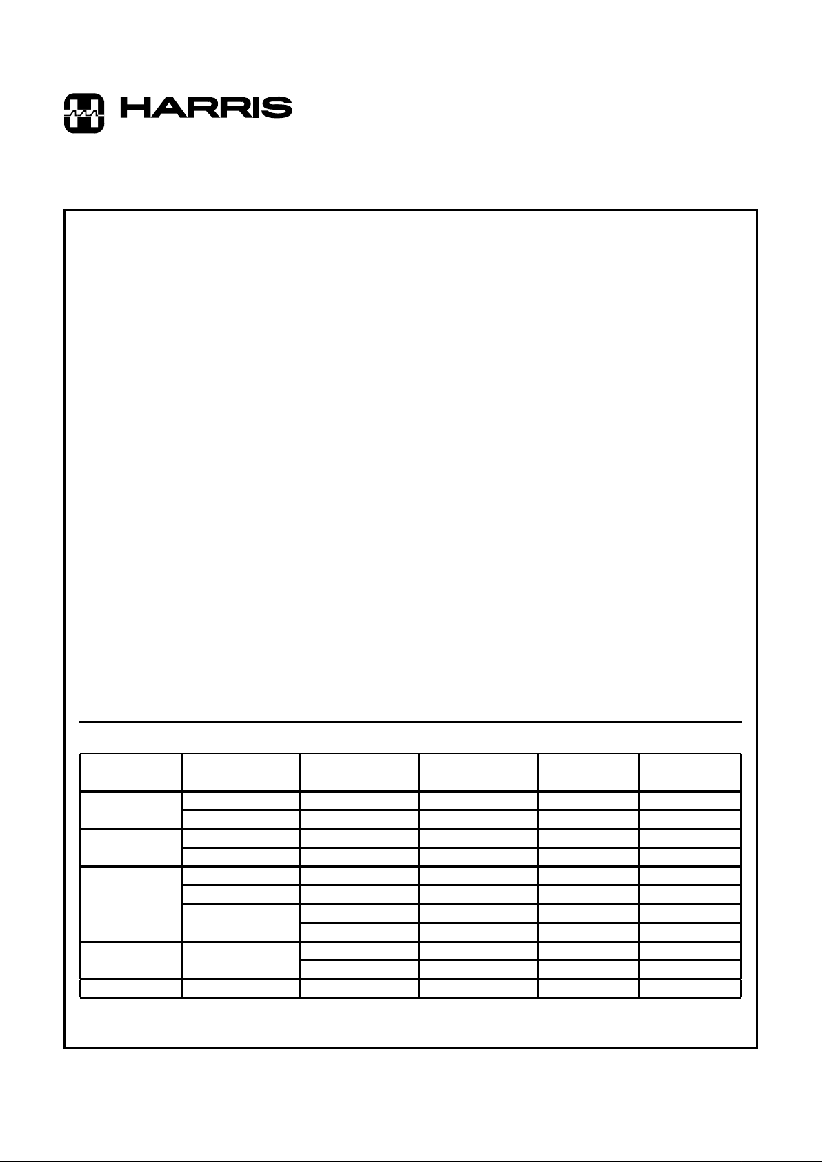
Ordering Information
PACKAGE
TEMPERATURE
RANGE 5MHz 8MHz 12.5MHz PKG. NO.
Plastic DIP 0oC to +70oC CP82C59A-5 CP82C59A CP82C59A-12 E28.6
-40oC to +85oC IP82C59A-5 IP82C59A IP82C59A-12 E28.6
PLCC 0oC to +70oC CS82C59A-5 CS82C59A CS82C59A-12 N28.45
-40oC to +85oC IS82C59A-5 IS82C59A IS82C59A-12 N28.45
CERDIP 0oC to +70oC CD82C59A-5 CD82C59A CD82C59A-12 F28.6
-40oC to +85oC ID82C59A-5 ID82C59A ID82C59A-12 F28.6
-55oC to +125oC MD82C59A-5/B MD82C59A/B MD82C59A-12/B F28.6
SMD# 5962-8501601YA 5962-8501602YA - F28.6
LCC -55oC to +125oC MR82C59A-5/B MR82C59A/B MR82C59A-12/B J28.A
SMD# 5962-85016013A 5962-85016023A - J28.A
SOIC 0oC to +70oC CM82C59A-5 CM82C59A CM82C59A-12 M28.3
CAUTION: These devices are sensitive to electrostatic discharge. Users should follow proper IC Handling Procedures.
Copyright
© Harris Corporation 1996
File Number 2784.2
Page 2
4-253
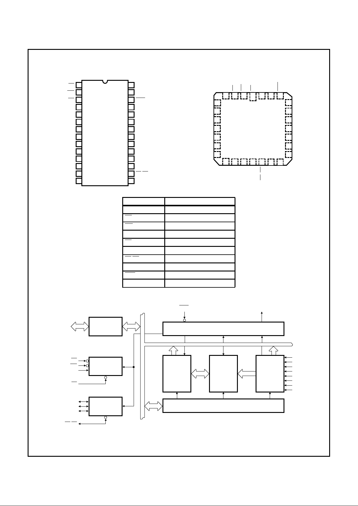
Functional Diagram
Pinouts
28 LEAD DIP
TOP VIEW
28 LEAD LCC
TOP VIEW
PIN DESCRIPTION
D7 - D0 Data Bus (Bidirectional)
RD Read Input
WR Write Input
A0 Command Select Address
CS Chip Select
CAS 2 - CAS 0 Cascade Lines
SP/EN Slave Program Input Enable
INT Interrupt Output
INTA Interrupt Acknowledge Input
IR0 - IR7 Interrupt Request Inputs
CS
WR
RD
D7
D6
D5
D4
D3
D2
D1
D0
CAS 0
CAS 1
GND
V
CC
INTA
IR7
IR6
IR5
IR3
IR1
IR0
INT
SP/EN
CAS 2
A0
IR4
IR2
28
27
26
25
24
23
22
21
20
19
18
17
16
15
1
2
3
4
5
6
7
8
9
10
11
12
13
14
23
24
25
22
21
20
19
11
3 2
1
4
14 15 16 17 18
12
13
28 27 26
10
5
6
7
8
9
D7
V
CC
A0
RD
WR
CS
INTA
D6
D5
D4
D3
D2
D1
D0
IR7
IR6
IR5
IR4
IR3
IR2
IR1
CAS 0
IR0
CAS 1
GND
CAS 2
SP/ EN
INT
PRIORITY
RESOLVER
IR0
IR1
IR2
IR3
IR4
IR5
IR6
IR7
INTERRUPT
REQUEST
REG
(IRR)
INTERRUPT MASK REG
(IMR)
CONTROL LOGIC
INTERNAL BUS
INT
DATA
BUS
BUFFER
CASCADE
BUFFER
COMPARATOR
CAS 0
CAS 1
CAS 2
READ/
WRITE
LOGIC
SP/EN
WR
RD
INTA
IN -
SERVICE
REG
(ISR)
CS
D
7-D0
A
0
FIGURE 1.
82C59A
Page 3
4-254
Functional Description
Interrupts in Microcomputer Systems
Microcomputer system design requires that I/O devices such
as keyboards, displays, sensors and other components
receive servicing in an efficient manner so that large
amounts of the total system tasks can be assumed by the
microcomputer with little or no effect on throughput.
The most common method of servicing such devices is the
Polled approach. This is where the processor must test each
device in sequence and in effect “ask” each one if it needs
servicing. It is easy to see that a large portion of the main
program is looping through this continuous polling cycle and
that such a method would have a serious, detrimental effect
on system throughput, thus, limiting the tasks that could be
assumed by the microcomputer and reducing the cost effectiveness of using such devices.
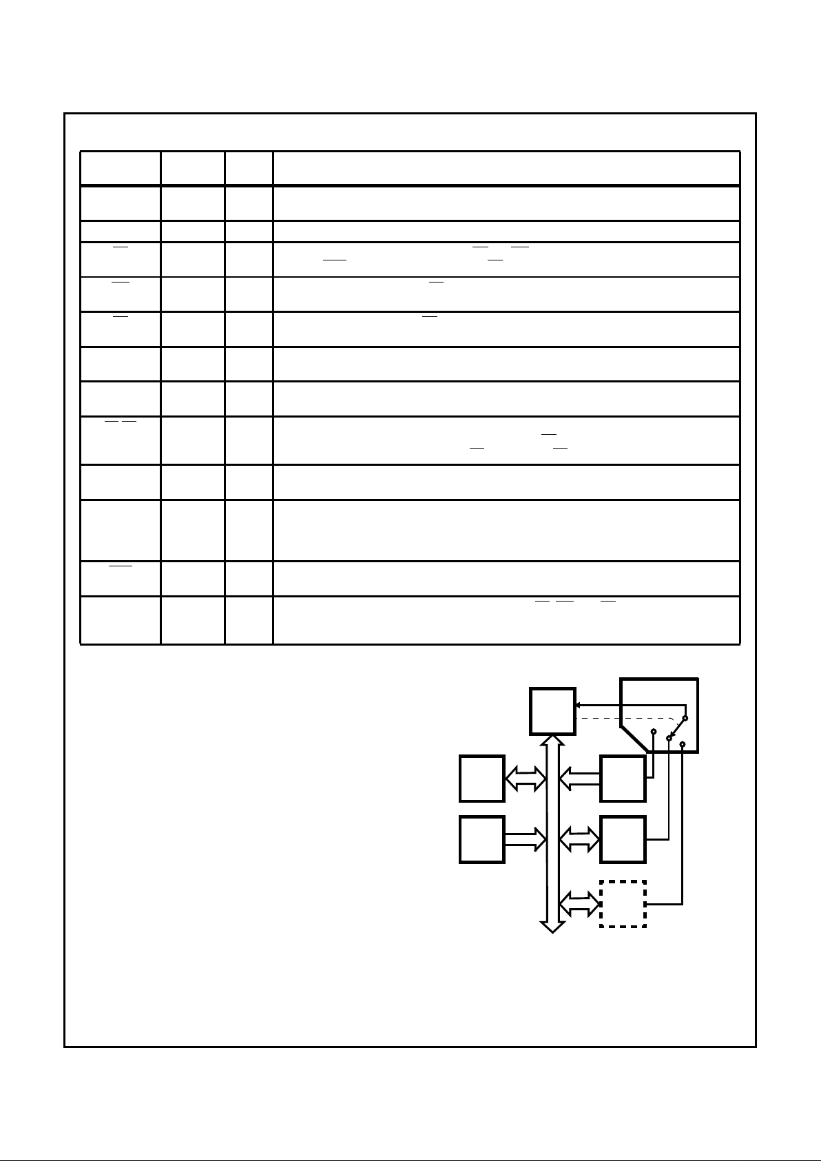
Pin Description
SYMBOL
PIN
NUMBER TYPE DESCRIPTION
V
CC
28 I VCC: The +5V power supply pin. A 0.1µF capacitor between pins 28 and 14 is recommended for
decoupling.
GND 14 I GROUND
CS 1 I CHIP SELECT: A low on this pin enablesRD and WR communications between the CPU and the
82C59A. INT A functions are independent ofCS.
WR 2 I WRITE: A low on this pin when CS is low enables the 82C59A to accept command words from
the CPU.
RD 3 I READ: A low on this pin when CS is low enables the 82C59A to release status onto the data bus
for the CPU.
D7 - D0 4 - 11 I/O BIDIRECTIONAL DATA BUS: Control, status, and interrupt-vector information is transferred via
this bus.
CAS0 - CAS2 12, 13, 15 I/O CASCADE LINES: The CAS lines form a private 82C59A bus to control a multiple 82C59A struc-
ture. These pins are outputs for a master 82C59A and inputs for a slave 82C59A.
SP/EN 16 I/O SLAVE PROGRAM/ENABLE BUFFER: This is a dual function pin. When in the Buffered Mode it
can be used as an output to control buffer transceivers (EN). When not in the Buffered Mode it is
used as an input to designate a master (SP = 1) or slave (SP = 0).
INT 17 O INTERRUPT: This pin goes high whenever a valid interrupt request is asserted. It is used to inter-
rupt the CPU, thus, it is connected to the CPU's interrupt pin.
IR0 - IR7 18 - 25 I INTERRUPT REQUESTS: Asynchronous inputs. An interrupt request is executed by raising an
IR input (low to high), and holding it high until it is acknowledged (Edge Triggered Mode), or just
by a high level on an IR input (Level Triggered Mode). Internal pull-up resistors are implemented
on IR0 - 7.
INTA 26 I INTERRUPT ACKNOWLEDGE: This pin is used to enable 82C59A interrupt-vector data onto the
data bus by a sequence of interrupt acknowledge pulses issued by the CPU.
A0 27 I ADDRESS LINE: This pin acts in conjunction with the CS, WR, and RD pins. It is used by the
82C59A to decipher various Command Words the CPU writes and status the CPU wishes to read.
It is typically connected to the CPU A0 address line (A1 for 80C86/88/286).
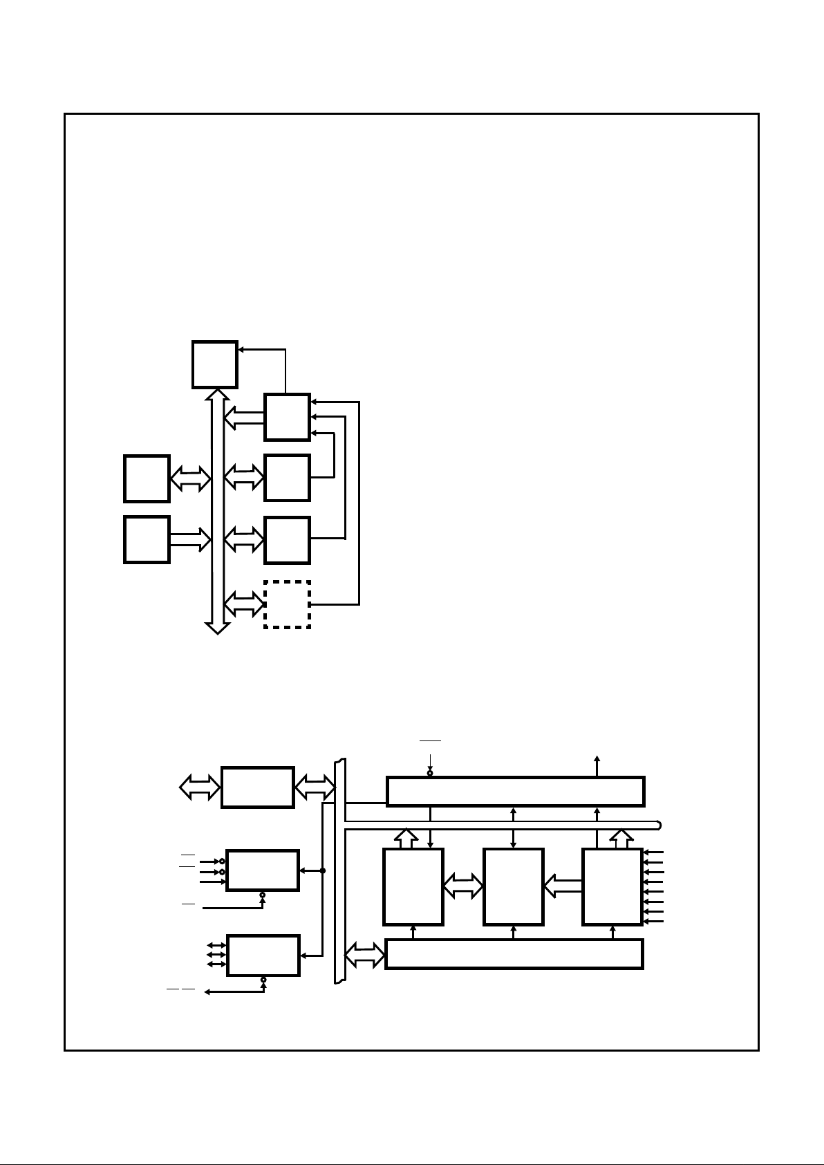
ROM
I/O (N)
I/O (2)
I/O (1)RAM
CPU
CPU - DRIVEN
MULTIPLEXER
FIGURE 2. POLLED METHOD
82C59A
Page 4
4-255
A more desirable method would be one that would allow the
microprocessor to be executing its main program and only
stop to service peripheral devices when it is told to do so by
the device itself. In effect, the method would provide an
external asynchronous input that would inform the processor
that it should complete whatever instruction that is currently
being executed and fetch a new routine that will service the
requesting device. Once this servicing is complete, however,
the processor would resume exactly where it left off.
This is the Interrupt-driven method. It is easy to see that system throughput would drastically increase, and thus, more
tasks could be assumed by the microcomputer to further
enhance its cost effectiveness.
The Programmable Interrupt Controller (PlC) functions as an
overall manager in an Interrupt-Driven system. It accepts
requests from the peripheral equipment, determines which
of the incoming requests is of the highest importance (priority), ascertains whether the incoming request has a higher
priority value than the level currently being serviced, and
issues an interrupt to the CPU based on this determination.
Each peripheral device or structure usually has a special
program or “routine” that is associated with its specific functional or operational requirements; this is referred to as a
“service routine”. The PlC, after issuing an interrupt to the
CPU, must somehow input information into the CPU that can
“point” the Program Counter to the service routine associated with the requesting device. This “pointer” is an address
in a vectoring table and will often be referred to, in this document, as vectoring data.
82C59A Functional Description
The 82C59A is a device specifically designed for use in real
time, interrupt driven microcomputer systems. It manages
eight levels of requests and has built-in features for expandability to other 82C59As (up to 64 levels). It is programmed
by system software as an I/O peripheral. A selection of priority modes is available to the programmer so that the manner
in which the requests are processed by the 82C59A can be
configured to match system requirements. The priority
modes can be changed or reconfigured dynamically at any
time during main program operation. This means that the
complete interrupt structure can be defined as required,
based on the total system environment.
Interrupt Request Register (IRR) and In-Service Register
(ISR)
The interrupts at the IR input lines are handled by two registers
in cascade, the Interrupt Request Register (lRR) and the InService Register (lSR). The IRR is used to indicate all the interrupt levels which are requesting service, and the ISR is used to
store all the interrupt levels which are currently being serviced.
ROM
I/O (2)
RAM
CPU
INT
I/O (1)
I/O (N)
PIC
FIGURE 3. INTERRUPT METHOD
IR0
IR1
IR2
CASCADE
BUFFER
COMPARATOR
READ/
WRITE
LOGIC
DAT A
BUS
BUFFER
IN
SERVICE
REG
(ISR)
PRIORITY
RESOLVER
INTERRUPT MASK REG
(IMR)
INTERRUPT
REQUEST
REG
(IRR)
CONTROL LOGIC
INT
INTA
IR3
IR4
IR5
IR6
IR7
CAS 0
CAS 1
CAS 2
RD
WR
A
0
SP/EN
CS
D
7
- D
0
INTERNAL BUS
FIGURE 4. 82C59A FUNCTIONAL DIAGRAM
82C59A
Page 5

4-256
Priority Resolver
This logic block determines the priorities of the bits set in the
lRR. The highest priority is selected and strobed into the corresponding bit of the lSR during the INTA sequence.
Interrupt Mask Register (IMR)
The lMR stores the bits which disable the interrupt lines to
be masked. The IMR operates on the output of the IRR.
Masking of a higher priority input will not affect the interrupt
request lines of lower priority.
Interrupt (INT)
This output goes directly to the CPU interrupt input. The
VOH level on this line is designed to be fully compatible with
the 8080, 8085, 8086/88, 80C86/88, 80286, and 80C286
input levels.
Interrupt Acknowledge (
INTA)
INTA pulses will cause the 82C59A to release vectoring
information onto the data bus. The format of this data
depends on the system mode (µPM) of the 82C59A.
Data Bus Buffer
This 3-state, bidirectional 8-bit buffer is used to interface the
82C59A to the System Data Bus. Control words and status
information are transferred through the Data Bus Buffer.
Read/Write Control Logic
The function of this block is to accept output commands from
the CPU. It contains the Initialization Command Word (lCW)
registers and Operation Command Word (OCW) registers
which store the various control formats for device operation.
This function block also allows the status of the 82C59A to
be transferred onto the Data Bus.
Chip Select (
CS)
A LOW on this input enables the 82C59A. No reading or
writing of the device will occur unless the device is selected.
Write (
WR)
A LOW on this input enables the CPU to write control words
(lCWs and OCWs) to the 82C59A.
Read (
RD)
A LOW on this input enables the 82C59A to send the status
of the Interrupt Request Register (lRR), In-Service Register
(lSR), the Interrupt Mask Register (lMR), or the interrupt
level (in the poll mode) onto the Data Bus.
A0
This input signal is used in conjunction with
WR and RD signals to write commands into the various command registers,
as well as to read the various status registers of the chip.
This line can be tied directly to one of the system address
lines.
The Cascade Buffer/Comparator
This function block stores and compares the IDs of all
82C59As used in the system. The associated three I/O pins
(CAS0 - 2) are outputs when the 82C59A is used as a master and are inputs when the 82C59A is used as a slave. As a
master, the 82C59A sends the ID of the interrupting slave
device onto the CAS0 - 2 lines. The slave, thus selected will
send its preprogrammed subroutine address onto the Data
Bus during the next one or two consecutive
INTA pulses.
(See section “Cascading the 82C59A”.)
Interrupt Sequence
The powerful features of the 82C59A in a microcomputer
system are its programmability and the interrupt routine
addressing capability. The latter allows direct or indirect
jumping to the specified interrupt routine requested without
any polling of the interrupting devices. The normal sequence
of events during an interrupt depends on the type of CPU
being used.
These events occur in an 8080/8085 system:
1. One or more of the INTERRUPT REQUEST lines
(IR0 - IR7) are raised high, setting the corresponding IRR
bit(s).
2. The 82C59A evaluates those requests in the priority
resolver and sends an interrupt (INT) to the CPU, if
appropriate.
3. The CPU acknowledges the lNT and responds with an
INTA pulse.
4. Upon receiving an
lNTA from the CPU group, the highest
priority lSR bit is set, and the corresponding lRR bit is
reset. The 82C59A will also release a CALL instruction
code (11001101) onto the 8-bit data bus through D0 - D7.
5. This CALL instruction will initiate two additional
INTA
pulses to be sent to 82C59A from the CPU group.
6. These two
INTA pulses allow the 82C59A to release its
preprogrammed subroutine address onto the data bus.
The lower 8-bit address is released at the first
INTA pulse
and the higher 8-bit address is released at the second
INTA pulse.
7. This completes the 3-byte CALL instruction released by
the 82C59A. In the AEOI mode, the lSR bit is reset at the
end of the third
INTA pulse. Otherwise, the lSR bit
remains set until an appropriate EOI command is issued
at the end of the interrupt sequence.
The events occurring in an 80C86/88/286 system are the
same until step 4.
4. The 82C59A does not drive the data bus during the first
INTA pulse.
5. The 80C86/88/286 CPU will initiate a second
INTA pulse.
During this
INTA pulse, the appropriate ISR bit is set and
the corresponding bit in the IRR is reset. The 82C59A
outputs the 8-bit pointer onto the data bus to be read by
the CPU.
82C59A
Page 6
4-257
6. This completes the interrupt cycle. In the AEOI mode, the
ISR bit is reset at the end of the second
INTA pulse. Otherwise, the ISR bit remains set until an appropriate EOI
command is issued at the end of the interrupt subroutine.
If no interrupt request is present at step 4 of either sequence
(i.e., the request was too short in duration), the 82C59A will
issue an interrupt level 7. If a slave is programmed on IR bit
7, the CAS lines remain inactive and vector addresses are
output from the master 82CS9A.
Interrupt Sequence Outputs
8080, 8085 Interrupt Response Mode
This sequence is timed by three
INTA pulses. During the first
lNTA pulse, the CALL opcode is enabled onto the data bus.
First Interrupt Vector Byte Data: Hex CD
During the second
INTA pulse, the lower address of the
appropriate service routine is enabled onto the data bus.
When interval = 4 bits, A5 - A7 are programmed, while
A0 - A4 are automatically inserted by the 82C59A. When
interval = 8, only A6 and A7 are programmed, while A0 - A5
are automatically inserted.
During the third
INTA pulse, the higher address of the appropriate service routine, which was programmed as byte 2 of the
initialization sequence (A8 - A15), is enabled onto the bus.
D7 D6 D5 D4 D3 D2 D1 D0
Call Code 11001101
ADDRESS BUS (16)
CONTROL BUS
DATA BUS (8)
I/OR I/OW INT INTA
CASCADE
LINES
CAS 0
CAS 1
CAS 2
SP/EN
CS RD WR INTAINTD7 - D
0
A
0
SLAVE PROGRAM/
ENABLE BUFFER
INTERRUPT
REQUESTS
82C59A
IRQ IRQ IRQ IRQ IRQ IRQ IRQ IRQ
7
6
5
4
3
2
1
0
FIGURE 5. 82C59A STANDARD SYSTEM BUS INTERFACE
CONTENT OF SECOND INTERRUPT VECTOR BYTE
IR Interval = 4
D7 D6 D5 D4 D3 D2 D1 D0
7A7A6A511100
6A7A6A511000
5A7A6A510100
4A7A6A510000
3A7A6A501100
2A7A6A501000
1A7A6A500100
0A7A6A500000
IR Interval = 8
D7 D6 DS D4 D3 D2 Dl DO
7A7A6111000
6A7A6110000
5A7A6101000
4A7A6100000
3A7A6011000
2A7A6010000
1A7A6001000
0A7A6000000
82C59A
Page 7

4-258
80C86, 8OC88, 80C286 Interrupt Response Mode
80C86/88/286 mode is similar to 8080/85 mode except that
only two Interrupt Acknowledge cycles are issued by the processor and no CALL opcode is sent to the processor. The
first interrupt acknowledge cycle is similar to that of 8080/85
systems in that the 82C59A uses it to internally freeze the
state of the interrupts for priority resolution and, as a master,
it issues the interrupt code on the cascade lines. On this first
cycle, it does not issue any data to the processor and leaves
its data bus buffers disabled. On the second interrupt
acknowledge cycle in the 86/88/286 mode, the master (or
slave if so programmed) will send a byte of data to the processor with the acknowledged interrupt code composed as
follows (note the state of the ADI mode control is ignored
and A5 - A11 are unused in the 86/88/286 mode).
Programming the 82C59A
The 82C59A accepts two types of command words generated by the CPU:
1. Initialization Command Words (ICWs): Before normal
operation can begin, each 82C59A in the system must be
brought to a starting point - by a sequence of 2 to 4 bytes
timed by
WR pulses.
2. Operation Command Words (OCWs): These are the
command words which command the 82C59A to operate
in various interrupt modes. Among these modes are:
a. Fully nested mode.
b. Rotating priority mode.
c. Special mask mode.
d. Polled mode.
The OCWs can be written into the 82C59A anytime after initialization.
Initialization Command Words (lCWs)
General
Whenever a command is issued with A0 = 0 and D4 = 1, this
is interpreted as Initialization Command Word 1 (lCW1).
lCW1 starts the initialization sequence during which the following automatically occur:
a. The edge sense circuit is reset, which means that follow-
ing initialization, an interrupt request (IR) input must make
a low-to-high transition to generate an interrupt.
b. The Interrupt Mask Register is cleared.
c. lR7 input is assigned priority 7.
d. Special Mask Mode is cleared and Status Read is set to
lRR.
e. If lC4 = 0, then all functions selected in lCW4 are set to
zero. (Non-Buffered mode (see note), no Auto-EOI,
8080/85 system).
NOTE: Master/Slave in ICW4 is only used in the buffered mode.
Initialization Command Words 1 and 2 (ICW1, lCW2)
A5 - A15: Page starting address of service routines. In an
8080/85 system the 8 request levels will generate CALLS to
8 locations equally spaced in memory. These can be programmed to be spaced at intervals of 4 or 8 memory locations, thus, the 8 routines will occupy a page of 32 or 64
bytes, respectively.
CONTENT OF THIRD INTERRUPT VECTOR BYTE
D7 D6 D5 D4 D3 D2 D1 D0
A15 A14 A13 A12 A11 A10 A9 A8
CONTENT OF INTERRUPT VECTOR BYTE FOR
80C86/88/286 SYSTEM MODE
D7 D6 D5 D4 D3 D2 D1 D0
lR7 T7 T6 T5 T4 T3 1 1 1
lR6 T7 T6 T5 T4 T3 1 1 0
IR5 T7 T6 T5 T4 T3 1 0 1
IR4 T7 T6 T5 T4 T3 1 0 0
IR3 T7 T6 T5 T4 T3 0 1 1
IR2 T7 T6 T5 T4 T3 0 1 0
IR1 T7 T6 T5 T4 T3 0 0 1
IR0 T7 T6 T5 T4 T3 0 0 0
ICW1
ICW2
IN
CASCADE
MODE
ICW3
IS ICW4
NEEDED
ICW4
READY TO ACCEPT
INTERRUPT REQUESTS
NO (SNGL = 1)
YES (SNGL = 0))
YES (IC4 = 1)
NO (IC4 = 0)
FIGURE 6. 82C59A INITIALIZATION SEQUENCE
82C59A
Page 8

4-259
D
7
A
O
D
6
D
5
D
4
D
3
D
2
D
1
D
0
0
A
7
A
6
A
5
LTIM1 ADI SNGL IC4
ICW1
1 = ICWR needed
0 = No ICW4 needed
1 = Single
0 = Cascade Mode
CALL address interval
1 = Interval of 4
0 = Interval of 8
1 = Level triggered mode
0 = Edge triggered mode
A
7
- A5 of Interrupt vector address
(MCS-80/85 mode only)
D
7
A
O
D
6
D
5
D
4
D
3
D
2
D
1
D
0
1
A
15
A
14
A
13
A
11
A
10
A
9
A
8
A
12
T
7
T
6
T
5
T
4
T
3
ICW2
A15 - A8 of interrupt vector address
(MCS80/85 mode)
T
7
- T3 of interrupt vector address
(8086/8088 mode)
D
7
A
O
D
6
D
5
D
4
D
3
D
2
D
1
D
0
1S
7
S
6
S
5
S
3
S
2
S
1
S
0
S
4
ICW3 (MASTER DEVICE)
1 = IR input has a slave
0 = IR input does not have a slave
D
7
A
O
D
6
D
5
D
4
D
3
D
2
D
1
D
0
1000 0ID
2ID1
ID
0
0
ICW3 (SLAVE DEVICE)
SLAVE ID (NOTE 1)
01 5234 67
01 1010 01
00 0110 11
00 1001 11
D
7
A
0
D6D
5
D4D
3
D2D1D
0
1 0 0 0 BUF M/S AEOI µPMSFNM
ICW4
1 = 8086/8088 mode
0 = MCS-80/85 mode
1 = Auto EOI
0 = Normal EOI
0
1
11
0
X- Non buffered mode
- Buffered mode slave
- Buffered mode master
1 = Special fully nested moded
0 = Not special fully nested mode
FIGURE 7. 82C59A INITIALIZATION COMMAND WORD FORMAT
NOTE: Slave ID is equal to the corresponding master IR input.
82C59A
Page 9

4-260
The address format is 2 bytes long (A0 - A15). When the
routine interval is 4, A0 - A4 are automatically inserted by
the 82C59A, while A5 - A15 are programmed externally.
When the routine interval is 8, A0 - A5 are automatically
inserted by the 82C59A while A6 - A15 are programmed
externally.
The 8-byte interval will maintain compatibility with current
software, while the 4-byte interval is best for a compact jump
table.
In an 80C86/88/286 system, A15 - A11 are inserted in the
five most significant bits of the vectoring byte and the
82C59A sets the three least significant bits according to the
interrupt level. A10 - A5 are ignored and ADI (Address interval) has no effect.
LTlM: If LTlM = 1, then the 82C59A will operate in the level
interrupt mode. Edge detect logic on the interrupt
inputs will be disabled.
ADI: ALL address interval. ADI = 1 then interval = 4; ADI
= 0 then interval = 8.
SNGL: Single. Means that this is the only 82C59A in the
system. If SNGL = 1, no ICW3 will be issued.
IC4: If this bit is set - lCW4 has to be issued. If lCW4 is
not needed, set lC4 = 0.
Initialization Command Word 3 (ICW3)
This word is read only when there is more than one 82C59A
in the system and cascading is used, in which case
SNGL = 0. It will load the 8-bit slave register. The functions of
this register are:
a. In the master mode (either when
SP = 1, or in buffered
mode when M/S = 1 in lCW4) a “1” is set for each slav e in
the bit corresponding to the appropriate IR line for the
slave. The master then will release byte 1 of the call
sequence (for 8080/85 system) and will enable the corresponding slave to release bytes 2 and 3 (for 80C86/88/
286, only byte 2) through the cascade lines.
b. In the slave mode (either when SP = 0, or if BUF = 1 and
M/S = 0 in lCW4), bits 2 - 0 identify the slave. The slave
compares its cascade input with these bits and if they are
equal, bytes 2 and 3 of the call sequence (or just byte 2 for
80C86/88/286) are released by it on the Data Bus.
NOTE: (The slave address must correspond to the IR line it is connected to in the master ID).
Initialization Command Word 4 (ICW4)
SFNM: If SFNM = 1, the special fully nested mode is pro-
grammed.
BUF: If BUF = 1, the buffered mode is programmed. In
buffered mode,
SP/EN becomes an enable output
and the master/slave determination is by M/S.
M/S: If buffered mode is selected: M/S = 1 means the
82C59A is programmed to be a master, M/S = 0
means the 82C59A is programmed to be a slave. If
BUF = 0, M/S has no function.
AEOI: If AEOI = 1, the automatic end of interrupt mode is
programmed.
µPM: Microprocessor mode: µPM = 0 sets the 82C59A for
8080/85 system operation, µPM = 1 sets the
82C59A for 80C86/88/286 system operation.
Operation Command Words (OCWs)
After the Initialization Command Words (lCWs) are programmed into the 82C59A, the device is ready to accept
interrupt requests at its input lines. However, during the
82C59A operation, a selection of algorithms can command
the 82C59A to operate in various modes through the Operation Command Words (OCWs).
Operation Control Word 1 (OCW1)
OCW1 sets and clears the mask bits in the Interrupt Mask
Register (lMR) M7 - M0 represent the eight mask bits. M = 1
indicates the channel is masked (inhibited), M = 0 indicates
the channel is enabled.
Operation Control Word 2 (OCW2)
R, SL, EOI - These three bits control the Rotate and End of
Interrupt modes and combinations of the two. A chart of
these combinations can be found on the Operation Command Word Format.
L2, L1, L0 - These bits determine the interrupt level acted
upon when the SL bit is active.
Operation Control Word 3 (OCW3)
ESMM - Enable Special Mask Mode. When this bit is set to 1
it enables the SMM bit to set or reset the Special Mask
Mode. When ESMN = 0, the SMM bit becomes a “don’t
care”.
SMM - Special Mask Mode. If ESMM = 1 and SMM = 1, the
82C59A will enter Special Mask Mode. If ESMM = 1 and
SMM = 0, the 82C59A will revert to normal mask mode.
When ESMM = 0, SMM has no effect.
Fully Nested Mode
This mode is entered after initialization unless another mode
is programmed. The interrupt requests are ordered in priority
from 0 through 7 (0 highest). When an interrupt is acknowledged the highest priority request is determined and its vector placed on the bus. Additionally, a bit of the Interrupt
Service register (ISO - 7) is set. This bit remains set until the
microprocessor issues an End of Interrupt (EOI) command
OPERATION CONTROL WORDS (OCWs)
AD D7 D6 D5 D4 D3 D2 D1 D0
OCW1
1 M7M6M5M4M3M2M1M0
OCW2
0 R SL EOI 0 0 L2 L1 L0
OCW3
0 0 ESSM SMM 0 1 P RR RIS
82C59A
Page 10

4-261
immediately before returning from the service routine, or if
the AEOI (Automatic End of Interrupt) bit is set, until the trailing edge of the last
INTA. While the IS bit is set, all further
interrupts of the same or lower priority are inhibited, while
higher levels will generate an interrupt (which will be
acknowledged only if the microprocessor internal interrupt
enable flip-flop has been re-enabled through software).
After the initialization sequence, IRO has the highest priority
and IR7 the lowest. Priorities can be changed, as will be
explained in the rotating priority mode or via the set priority
command.
D
7
A
O
D
6
D
5
D
4
D
3
D
2
D
1
D
0
1M
7
M
6
M
5
M
3
M
2
M
1
M
0
M
4
OCW1
Interrupt Mask
1 = Mask set
0 = Mask reset
D
7
A
O
D
6
D
5
D
4
D
3
D
2
D
1
D
0
1 R SL EOI 0 L
2
L
1
L
0
0
OCW2
IR LEVEL TO BE
01 5234 67
01 1010 01
00 0110 11
00 1001 11
001
011
101
100
0
1
1
0
0
1
1
10
0
1
0
Non specific EOI command
Specific EOI command
Rotate on non specific EOI command
Rotate in automatic EOI mode (set)
Rotate in automatic EOI mode (clear)
Rotate on specific EOI command
Set priority command
No operation
†
†
†
ACTED UPON
End of interrupt
Automatic rotation
Specific rotation
† L
0
- L2 are used
D
7
A
O
D
6
D
5
D
4
D
3
D
2
D
1
D
0
0 0 ESMM SMM 1 P RR R1S0
OCW3
0011
1100
No Action
Read IR reg on
next RD pulse
Read IS reg on
next
RD pulse
1 = Poll command
0 = No poll command
0011
1100
No Action
Reset special
mask
Set special
mask
READ REGISTER COMMAND
FIGURE 8. 82C59A OPERATION COMMAND WORD FORMAT
SPECIAL MASK MODE
82C59A
Page 11

4-262
End of Interrupt (EOI)
The In-Service (IS) bit can be reset either automatically following the trailing edge of the last in sequence
INTA pulse
(when AEOI bit in lCW1 is set) or by a command word that
must be issued to the 82C59A before returning from a service routine (EOI Command). An EOI command must be
issued twice if servicing a slave in the Cascade mode, once
for the master and once for the corresponding slave.
There are two forms of EOl command: Specific and NonSpecific. When the 82C59A is operated in modes which preserve the fully nested structure, it can determine which IS bit
to reset on EOI. When a Non-Specific command is issued
the 82C59A will automatically reset the highest IS bit of
those that are set, since in the fully nested mode the highest
IS level was necessarily the last level acknowledged and
serviced. A nonspecific EOI can be issued with OCW2
(EOl = 1, SL = 0, R = 0).
When a mode is used which may disturb the fully nested
structure, the 82C59A may no longer be able to determine
the last level acknowledged. In this case a Specific End of
Interrupt must be issued which includes as part of the command the IS level to be reset. A specific EOl can be issued
with OCW2 (EOI = 1, SL = 1, R = 0, and LO - L2 is the binary
level of the IS bit to be reset).
An lRR bit that is masked by an lMR bit will not be cleared by
a nonspecific EOI if the 82C59A is in the Special Mask
Mode.
Automatic End of Interrupt (AEOI) Mode
If AEOI = 1 in lCW4, then the 82C59A will operate in AEOl
mode continuously until reprogrammed by lCW4. In this
mode the 82C59A will automatically perform a nonspecific
EOI operation at the trailing edge of the last interrupt
acknowledge pulse (third pulse in 8080/85, second in
80C86/88/286). Note that from a system standpoint, this
mode should be used only when a nested multilevel interrupt
structure is not required within a single 82C59A.
Automatic Rotation (Equal Priority Devices)
In some applications there are a number of interrupting
devices of equal priority. In this mode a device, after being
serviced, receives the lowest priority, so a device requesting
an interrupt will have to wait, in the worst case until each of 7
other devices are serviced at most once. For example, if the
priority and “in service” status is:
Before Rotate (lR4 the highest priority requiring service)
After Rotate (lR4 was serviced, all other priorities rotated
correspondingly)
There are two ways to accomplish Automatic Rotation using
OCW2, the Rotation on Non-Specific EOI Command (R = 1,
SL = 0, EOI = 1) and the Rotate in Automatic EOI Mode
which is set by (R = 1, SL = 0, EOI = 0) and cleared by
(R = 0, SL = 0, EOl = 0).
Specific Rotation (Specific Priority)
The programmer can change priorities by programming the
lowest priority and thus, fixing all other priorities; i.e., if IR5 is
programmed as the lowest priority device, then IR6 will have
the highest one.
The Set Priority command is issued in OCW2 where: R = 1,
SL = 1, L0 - L2 is the binary priority level code of the lowest
priority device.
Observe that in this mode internal status is updated by software control during OCW2. Howev er, it is independent of the
End of Interrupt (EOI) command (also executed by OCW2).
Priority changes can be executed during an EOI command
by using the Rotate on Specific EOl command in OCW2
(R = 1, SL = 1, EOI = 1, and LO - L2 = IR level to receive lo west priority).
Interrupt Masks
Each Interrupt Request input can be masked individually by
the Interrupt Mask Register (IMR) programmed through
OCW1. Each bit in the lMR masks one interrupt channel if it
is set (1). Bit 0 masks IRO, Bit 1 masks IR1 and so forth.
Masking an IR channel does not affect the operation of other
channels.
Special Mask Mode
Some applications may require an interrupt service routine
to dynamically alter the system priority structure during its
execution under software control. For example, the routine
may wish to inhibit lower priority requests for a portion of its
execution but enable some of them for another portion.
The difficulty here is that if an Interrupt Request is acknowledged and an End of Interrupt command did not reset its IS
bit (i.e., while executing a service routine), the 82C59A
would have inhibited all lower priority requests with no easy
way for the routine to enable them.
That is where the Special Mask Mode comes in. In the Special Mask Mode, when a mask bit is set in OCW1, it inhibits
further interrupts at that level and enables interrupts from all
other levels (lower as well as higher) that are not masked.
Thus, any interrupts may be selectively enabled by loaning
the mask register.
IS7 1S6 IS5 IS4 1S3 IS2 IS1 IS0
“IS” Status 0 1010000
Priority
Status
76543210
lowest highest
IS7 IS6 IS5 IS4 IS3 IS2 IS1 IS0
“IS” Status 01000000
Priority
Status
21076543
highest lowest
82C59A
Page 12

4-263
The special Mask Mode is set by OCW3 where: ESSM = 1,
SMM = 1, and cleared where ESSM = 1, SMM = 0.
Poll Command
In this mode, the INT output is not used or the microprocessor internal Interrupt Enable flip flop is reset, disabling its
interrupt input. Service to devices is achieved by software
using a Poll command.
The Poll command is issued by setting P = 1 in OCW3. The
82C59A treats the next
RD pulse to the 82C59A (i.e., RD =
0,
CS = 0) as an interrupt acknowledge, sets the appropriate
IS bit if there is a request, and reads the priority level. Interrupt is frozen from
WR to RD.
The word enabled onto the data bus during
RD is:
W0 - W2: Binary code of the highest priority level request-
ing service.
I: Equal to a “1” if there is an interrupt.
This mode is useful if there is a routine command common to
several levels so that the
INTA sequence is not needed (saves
ROM space). Another application is to use the poll mode to
expand the number of priority levels to more than 64.
Reading the 82C59A Status
The input status of several internal registers can be read to
update the user information on the system. The following
registers can be read via OCW3 (lRR and ISR) or OCW1
(lMR).
Interrupt Request Register (IRR): 8-bit register which contains the levels requesting an interrupt to be acknowledged.
The highest request level is reset from the lRR when an
interrupt is acknowledged. lRR is not affected by lMR.
In-Service Register (ISR): 8-bit register which contains the
priority levels that are being serviced. The ISR is updated
when an End of Interrupt Command is issued.
Interrupt Mask Register: 8-bit register which contains the
interrupt request lines which are masked.
The lRR can be read when, prior to the
RD pulse, a Read
Register Command is issued with OCW3 (RR = 1, RIS = 0).
The ISR can be read when, prior to the
RD pulse, a Read
Register Command is issued with OCW3 (RR = 1, RIS = 1).
There is no need to write an OCW3 before every status read
operation, as long as the status read corresponds with the
previous one: i.e., the 82C59A “remembers” whether the lRR
or ISR has been previously selected by the OCW3. This is
not true when poll is used. In the poll mode, the 82C59A
D7 D6 D5 D4 D3 D2 D1 D0
1----W2W1W0
EDGE
SENSE
LATCH
LTIM BIT
0 = EDGE
1 = LEVEL
V
CC
IR
8080/85
MODE
80C86/
88/286
MODE
INTA
FREEZE
INTA
FREEZE
FREEZE READ
IRR
WRITE
MASK
READ IMR
READ ISR
MASTER CLEAR
MASK LATCH
REQUEST
LATCH
IN - SERVICE
LATCH
NONMASKED
REQ
CLR
Q
SET
TO OTHER PRIORITY CELLS
PRIORITY
RESOLVER
CONTROL
LOGIC
SET ISR
CLR ISR
ISR BIT
QD
C
CLR
QD
CQ
CLR
SET
Q
NOTES:
1. Master clear active only during ICW1.
2. Freeze is active during INTA and poll sequence only.
3. Truth Table for D-latch.
C D Q Operation
1 D1 D1 Follow
0 X Qn-1 Hold
FIGURE 9. PRIORITY CELL - SIMPLIFIED LOGIC DIAGRAM
82C59A
Page 13

4-264
treats the
RD following a “poll write” operation as an INTA.
After initialization, the 82C59A is set to lRR.
For reading the lMR, no OCW3 is needed. The output data bus
will contain the lMR whenever
RD is active and A0 = 1 (OCW1).
Polling ov errides status read when P = 1, RR = 1 in OCW3.
Edge and Level Triggered Modes
This mode is programmed using bit 3 in lCW1.
If LTlM = “0”, an interrupt request will be recognized by a low to
high transition on an IR input. The IR input can remain high
without generating another interrupt.
If LTIM = “1”, an interrupt request will be recognized by a “high”
level on an IR input, and there is no need f or an edge detection.
The interrupt request must be removed before the EOI command is issued or the CPU interrupt is enabled to prevent a
second interrupt from occurring.
The priority cell diagram shows a conceptual circuit of the level
sensitive and edge sensitive input circuitry of the 82C59A. Be
sure to note that the request latch is a transparent D type latch.
In both the edge and level triggered modes the IR inputs
must remain high until after the falling edge of the first
INTA.
If the IR input goes low before this time a DEFAULT lR7 will
occur when the CPU acknowledges the interrupt. This can
be a useful safeguard for detecting interrupts caused by spurious noise glitches on the IR inputs. To implement this feature the lR7 routine is used for “clean up” simply executing a
return instruction, thus, ignoring the interrupt. If lR7 is
needed for other purposes a default lR7 can still be detected
by reading the ISR. A normal lR7 interrupt will set the corresponding ISR bit, a default IR7 won’t. If a default IR7 routine
occurs during a normal lR7 routine, however, the ISR will
remain set. In this case it is necessary to keep track of
whether or not the IR7 routine was previously entered. If
another lR7 occurs it is a default.
In power sensitive applications, it is advisable to place the
82C59A in the edge-triggered mode with the IR lines normally high. This will minimize the current through the internal
pull-up resistors on the IR pins.
The Special Fully Nested Mode
This mode will be used in the case of a big system where
cascading is used, and the priority has to be conserved
within each slave. In this case the special fully nested mode
will be programmed to the master (using lCW4). This mode
is similar to the normal nested mode with the following
exceptions:
a. When an interrupt request from a cer tain slave is in ser-
vice, this slave is not locked out from the master’s priority
logic and further interrupt requests from higher priority
IRs within the slave will be recognized by the master and
will initiate interrupts to the processor. (In the normal
nested mode a slave is masked out when its request is in
service and no higher requests from the same slave can
be serviced.
b. When exiting the Interrupt Service routine the software
has to check whether the interrupt serviced was the only
one from that slave. This is done by sending a nonspecific
End of Interrupt (EOI) command to the slave and then
reading its In-Service register and checking for zero. If it
is empty, a non-specified EOI can be sent to the master,
too. If not, no EOI should be sent.
Buffered Mode
When the 82C59A is used in a large system where bus driving buffers are required on the data bus and the cascading
mode is used, there exists the problem of enabling buffers
The buffered mode will structure the 82C59A to send an
enable signal on
SP/EN to enable the buffers. In this mode,
whenever the 82C59A’s data bus outputs are enabled, the
SP/EN output becomes active.
LATCH
ARM
(NOTE 1)
EARLIEST IR
CAN BE
REMOVED
LATCH
ARM
(NOTE 1)
8080/85
LATCH
ARM
(NOTE 1)
80C86/88/286
80C86/88/286
8080/85
IR
INT
INTA
NOTE:
1. Edge triggered mode only.
FIGURE 10. IR TRIGGERING TIMING REQUIREMENTS
82C59A
Page 14

4-265
This modification forces the use of software programming to
determine whether the 82C59A is a master or a slave. Bit 3
in ICW4 programs the buffered mode, and bit 2 in lCW4
determines whether it is a master or a slave.
Cascade Mode
The 82C59A can be easily interconnected in a system of
one master with up to eight slaves to handle up to 64 priority
levels.
The master controls the slaves through the 3 line cascade
bus (CAS2 - 0). The cascade bus acts like chip selects to the
slaves during the
INTA sequence.
In a cascade configuration, the slave interrupt outputs (INT)
are connected to the master interrupt request inputs. When
a slave request line is activated and afterwards acknowledged, the master will enable the corresponding slave to
release the device routine address during bytes 2 and 3 of
INTA. (Byte 2 only for 80C86/88/286).
The cascade bus lines are normally low and will contain the
slave address code from the leading edge of the first INTA
pulse to the trailing edge of the last
INTA pulse. Each
82C59A in the system must follow a separate initialization
sequence and can be programmed to work in a different
mode. An EOI command must be issued twice: once for the
master and once for the corresponding slave. Chip select
decoding is required to activate each 82C59A.
NOTE: Auto EOI is supported in the slave mode for the 82C59A.
The cascade lines of the Master 82C59A are activated only
for slave inputs, non-slave inputs leave the cascade line
inactive (low). Therefore, it is necessary to use a slave
address of 0 (zero) only after all other addresses are used.
FIGURE 11. CASCADING THE 82C59A
CS
82C59A
SLAVE A
CAS 0
CAS 1
CAS 2
INTA0D7 - D0INTA
SP/EN 7 56 43210
GND
756 43210
CS
82C59A
SLAVE B
CAS 0
CAS 1
CAS 2
INTA0D7 - D0INTA
SP/EN 7 56 43210
GND
756 43210
CS
MASTER 82C59A
CAS 0
CAS 1
CAS 2
INTA0D7 - D0INTA
SP/EN 7 56 43210
V
CC
75421036
INT REQ
DATA BUS (8)
CONTROL BUS
ADDRESS BUS (16)
INTERRUPT REQUESTS
82C59A
Page 15

4-266
Absolute Maximum Ratings Thermal Information
Supply Voltage . . . . . . . . . . . . . . . . . . . . . . . . . . . . . . . . . . . . .+8.0V
Input, Output or I/O Voltage . . . . . . . . . . . . GND-0.5V to VCC+0.5V
ESD Classification . . . . . . . . . . . . . . . . . . . . . . . . . . . . . . . . . Class I
Operating Conditions
Operating Voltage Range . . . . . . . . . . . . . . . . . . . . . +4.5V to +5.5V
Operating Temperature Range. . . . . . . . . . . . . . . .-55oC to +125oC
Input Low Voltage. . . . . . . . . . . . . . . . . . . . . . . . . . . . . . 0V to +0.8V
Thermal Resistance (Typical) θJA (oC/W) θJC (oC/W)
CERDIP Package . . . . . . . . . . . . . . . . 47.0 10
Ceramic LCC Package . . . . . . . . . . . . 55.0 9.0
Plastic DIP Package . . . . . . . . . . . . . . 55 -
Plastic LCC Package. . . . . . . . . . . . . . 65 -
Plastic SOIC Package. . . . . . . . . . . . . 75 -
Storage Temperature Range. . . . . . . . . . . . . . . . . .-65oC to +150oC
Maximum Junction Temperature Ceramic Package . . . . . . .+175oC
Maximum Junction Temperature Plastic Package. . . . . . . . .+150oC
Maximum Lead Temperature Ceramic Package . . . . . . . . . .+300oC
(Soldering 10s)
Maximum Lead Temperature Plastic Package . . . . . . . . . . .+260oC
(Soldering 10s)
Die Characteristics
Gate Count . . . . . . . . . . . . . . . . . . . . . . . . . . . . . . . . . . .1250 Gates
CAUTION: Stresses above those listed in “Absolute Maximum Ratings” may cause permanent damage to the device. This is a stress only rating and operation
of the device at these or any other conditions above those indicated in the operational sections of this specification is not implied.
DC Electrical Specifications V
CC
= +5.0V ±10%, TA = 0oC to +70oC (C82C59A), TA = -40oC to +85oC (I82C59A), TA = -55oC to
+125oC (M82C59A)
SYMBOL PARAMETER MIN MAX UNITS TEST CONDITIONS
V
lH
Logical One Input Voltage 2.0
2.2
-V
V
C82C59A, I82C59A
M82C59A
V
IL
Logical Zero Input Voltage - 0.8 V
V
OH
Output HIGH Voltage 3.0
VCC -0.4
-V
V
I
OH
= -2.5mA
lOH = -100µA
V
OL
Output LOW Voltage - 0.4 V lOL = +2.5mA
II Input Leakage Current -1.0 +1.0 µAVIN = GND or VCC, Pins 1-3, 26-27
IO Output Leakage Current -10.0 +10.0 µAV
OUT
= GND or VCC, Pins 4-13, 15-16
ILIR IR Input Load Current -
-
-200
10
µAµAVIN = 0V
VIN = V
CC
lCCSB Standby Power Supply Current - 10 µAVCC = 5.5V, VIN = VCC or GND Outputs
Open, (Note 1)
ICCOP Operating Power Supply Current - 1 mA/MHz VCC = 5.0V, CLK FREQ = 5MHz, VIN = VCC or GND,
Outputs Open, TA = 25oC, (Note 2)
NOTES:
1. Except for IR0 - lR7 where VIN = VCCor open.
2. ICCOP = 1mA/MHz of peripheral read/write cycle time. (ex: 1.0µs I/O read/write cycle time = 1mA).
Capacitance T
A
= +25oC
SYMBOL PARAMETER TYP UNITS TEST CONDITIONS
CIN Input Capacitance 15 pF FREQ = 1MHz, all measurements reference to
device GND.
COUT Output Capacitance 15 pF
CI/O I/O Capacitance 15 pF
82C59A
Page 16

4-267
AC Electrical Specifications V
CC
= +5.0V ±10%, GND = 0V, TA = 0oC to +70oC (C82C59A), TA -40oC to +85oC (l82C59A),
TA = -55oC to +125oC (M82C59A)
SYMBOL PARAMETER
82C59A-5 82C59A 82C59A-12
UNITS
TEST
CONDITIONSMIN MAX MIN MAX MIN MAX
TIMING REQUIREMENTS
(1) THRL A0/
CS Setup to RD/INTA 10 - 10 - 5 - ns
(2) TRHAX A0/CS Hold after RD/INTA 5-5-0- ns
(3) TRLRH RD/lNTA Pulse Width 235 - 160 - 60 - ns
(4) TAHWL A0/CS Setup to WR 0-000- ns
(5) TWHAX A0/CS Hold after WR 5-5-0- ns
(6) TWLWH WR Pulse Width 165 - 95 - 60 - ns
(7) TDVWH Data Setup to WR 240 - 160 - 70 - ns
(8) TWHDX Data Hold after WR 5-5-0- ns
(9) TJLJH Interrupt Request Width Low 100 - 100 - 40 - ns
(10) TCVlAL Cascade Setup to Second or Third INTA
Slave Only
55 - 40 - 30 - ns
(11) TRHRL EndofRD to next RD, End ofINT A within an
INT A sequence only
160 - 160 - 90 - ns
(12) TWHWL End of WR to next WR 190 - 190 - 60 - ns
(13) TCHCL
(Note 1)
End of Command to next command not
same command type), End of INTA
sequence to next INTA sequence
500 - 400 - 90 - ns
TIMING RESPONSES
(14) TRLDV Data Valid from RD/INTA - 160 - 120 - 40 ns 1
(15) TRHDZ Data Float after RD/INTA 5 100 5 85 5 22 ns 2
(16) TJHlH Interrupt Output Delay - 350 - 300 - 90 ns 1
(17) TlALCV Cascade Valid from First INTA
(Master Only)
- 565 - 360 - 50 ns 1
(18) TRLEL Enable Active from RD or INTA - 125 - 100 - 40 ns 1
(19) TRHEH Enable Inactive from RD or INTA - 60 - 50 - 22 ns 1
(20) TAHDV Data Valid from Stable Address - 210 - 200 - 60 ns 1
(21) TCVDC Cascade Valid to Valid Data - 300 - 200 - 70 ns 1
NOTE:
1. Worst case timing for TCHCL in an actual microprocessor system is typically greater than the values specified for the 82C59A,
(i.e. 8085A = 1.6µs, 8085A -2 = 1µs, 80C86 = 1µs, 80C286 -10 = 131ns, 80C286 -12 = 98ns).
82C59A
Page 17

4-268
AC Test Circuit
AC Testing Input, Output Waveform
TEST CONDITION DEFINITION TABLE
TEST
CONDITION V
1
R
1
R
2
C
1
1 1.7V 523Ω Open 100pF
2VCC1.8kΩ 1.8kΩ 50pF
V
1
R
1
R
2
C
1
(NOTE)
OUTPUT FROM
DEVICE UNDER
TEST
TEST
POINT
NOTE: Includes stray and jig capacitance.
Timing Waveforms
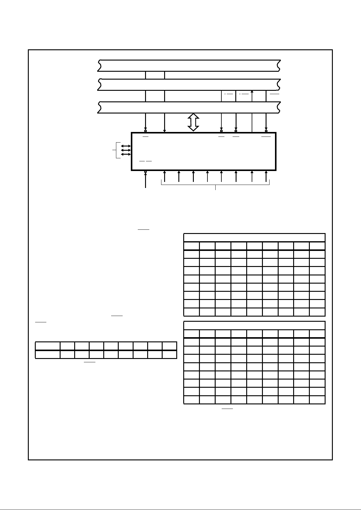
FIGURE 12. WRITE
INPUT
V
IH
+0.4V
V
IL
- 0.4V
1.5V
V
OH
OUTPUT
V
OL
1.5V
NOTE: AC Testing: All input signals must switch between VIL - 0.4V and VIH + 0.4V. Input rise and fall times are driven at 1ns/V.
WR
CS
ADDRESS BUS
A
0
DATA BUS
(7)
TDVWH
(8)
TWHDX
(4)
TAHWL
(5)
TWHAX
(6)
TWLWH
82C59A
Page 18

4-269
FIGURE 13. READ/INTA
FIGURE 14. OTHER TIMING
NOTES:
1. Interrupt Request (IR) must remain HIGH until leading edge of first
INTA.
2. During first INTA the Data Bus is not active in 80C86/88/286 mode.
3. 80C86/88/286.
4. 8080/8085 mode.
FIGURE 15. INTA SEQUENCE
Timing Waveforms
(Continued)
RD/INTA
EN
CS
ADDRESS BUS
DATA BUS
(20)
TAHDV
(14)
TRLDV
(1)
TAHRL
(18)
TRLEL
(3)
TRLRH
(19)
TRHEH
(2)
TRHAX
(15)
TRHDZ
A
0
(11)
TRHRL
(12)
TWHWL
(13)
TCHCL
RD
INTA
WR
RD
INTA
WR
RD
INTA
WR
IR
(9)
TJLJH
INT
INTA
SEE NOTE 1
DB
CAS 0 - 2
TCVIAL
(10)
SEE
NOTE 2
(17)
TIALCV
(21)
TCVDV
(10)
TCVIAL
SEE NOTE 3 SEE NOTE 4
(16)
TJHIH
82C59A
Page 19

4-270
Burn-In Circuits
MD82C59A CERDIP
MR82C59A CERAMIC LCC
R1
R1
R1
R1
R1
R1
R1
R1
R1
R1
R1
R3
R3
V
CC
R1
R2
R2
R2
R2
R2
R2
R3
R3
R1
R2
R2
28
27
26
25
24
23
22
21
20
19
18
17
16
15
1
2
3
4
5
6
7
8
9
10
11
12
13
14
C1
INTA
IR7
IR6
IR5
IR3
IR1
IR0
A
SP/EN
CAS 2
A0
IR4
IR2
WR
RD
D7
D6
D4
D2
D1
D0
CAS 0
CAS 1
GND
D5
D3
GND
V
CC
A
R3
R3
23
24
25
22
21
20
19
11
3 2 14
14 15 16 17 1812 13
28 27 26
10
5
6
7
8
9
CAS0
CAS1
GND
CAS2
SP/EN
IR0
V
CC
/2
R2
R2
R2
R2
R2
R2
R2
IR6
IR5
IR4
IR1
IR7
IR3
IR2
R1
R1
R1
R1
R1
R1
R1
D5
D4
D3
D0
D6
D2
D1
R1 R1 R1 R1 R4 R2
R1 R1 R1R1 R1 R1
D7 RD WR GND A0 INTA
VCCC1
NOTES:
1. VCC = 5.5V ±0.5V.
2. VIH = 4.5V ±10%.
3. VIL = -0.2V to 0.4V.
4. GND = 0V.
5. R1 = 47kΩ±5%.
6. R2 = 510Ω±5%.
7. R3 = 10Ω±5%.
8. R4 = 1.2kΩ±5%.
9. C1 = 0.01µF min.
10. F0 = 100kHz ±10%.
11. F1 = F0/2, F2 = F1/2, ...F8 = F7/2.
82C59A
Page 20

4-271
All Harris Semiconductor products are manufactured, assembled and tested under ISO9000 quality systems certification.
Harris Semiconductor products are sold by description only. Harris Semiconductor reserves the right to make changes in circuit design and/or specifications at
any time without notice. Accordingly, the reader is cautioned to verify that data sheets are current before placing orders. Information furnished by Harris is
believed to be accurate and reliable. However, no responsibility is assumed by Harris or its subsidiaries for its use; nor for any infringements of patents or other
rights of third parties which may result from its use. No license is granted by implication or otherwise under any patent or patent rights of Harris or its subsidiaries.
Sales Office Headquarters
For general information regarding Harris Semiconductor and its products, call 1-800-4-HARRIS
NORTH AMERICA
Harris Semiconductor
P. O. Box 883, Mail Stop 53-210
Melbourne, FL 32902
TEL: 1-800-442-7747
(407) 729-4984
FAX: (407) 729-5321
EUROPE
Harris Semiconductor
Mercure Center
100, Rue de la Fusee
1130 Brussels, Belgium
TEL: (32) 2.724.2111
FAX: (32) 2.724.22.05
ASIA
Harris Semiconductor PTE Ltd.
No. 1 Tannery Road
Cencon 1, #09-01
Singapore 1334
TEL: (65) 748-4200
FAX: (65) 748-0400
SEMICONDUCTOR
Die Characteristics
DIE DIMENSIONS: 143 x 130 x 19 ±1mils
METALLIZATION:
Type: Si-Al-Cu
Thickness: Metal 1: 8k
Å ± 0.75kÅ
Metal 2: 12kÅ ± 1.0kÅ
GLASSIVATION:
Type: Nitrox
Thickness: 108k
Å ± 3.0kÅ
Metallization Mask Layout
82C59A
D7
RD
WR
CS
V
CC
INTA
CAS0
CAS1
GND
CAS2
SP/EN
INT
D0 D1 D2 D3
D4 D5
IR1 IR2 IR3 IR4 IR5 IR6
A0
D6
IR0
IR7
82C59A
 Loading...