

Page 1
PD-60325
iP2005APbF
High Frequency Synchronous Buck
Optimized LGA Power Stage
Integrated Power Semiconductors, Driver IC, & Passives
Features
• 40A Multiphase building block
• No de-rating up to T
PCB
= 95ºC
• Optimized for low power loss
• Optimized for low EMI
• Bias supply range of 4.5V to 7.0V
• Operation up to 1.5MHz
• Bi-directional Current flow
• Under Voltage Lockout
• LGA interface
• 7.65mm x 7.65mm outline
Description
The iP2005A is a fully optimized solution for high curr ent
synchronous buck multiphase applications. Board space
and design time are greatly reduced because most of
the components required for each phase of a typical
discrete-based multiphase circuit are integrated into a
single 7.65mm x 7.65mm x 1.66mm power block. The
additional components required for a complete
multiphase converter are a PWM controller, the output
inductors, and the input and output capacitors.
iPOWIR Technology offers designers an innovative
board space saving solution for applications requiring
high power densities. iPOWIR technology eases design
for applications where component integration offers
benefits in performance and functionality. iPOWIR
technology solutions are also optimized internally for
layout, heat transfer, and component selection.
Applications
• High Frequency, Low Profile DC-DC
• Multi-phase Architectures
• Low Duty Cycle, High Current solutions
• Microprocessor Power Supplies
• General DC/DC Converters
Package
Description
Interface
Connection
Standard
Quantity
T & R
Orientation
iP2005APbF LGA 10 N/A
iP2005ATRPbF LGA 2000 Figure 15
2/8/2008www.irf.com
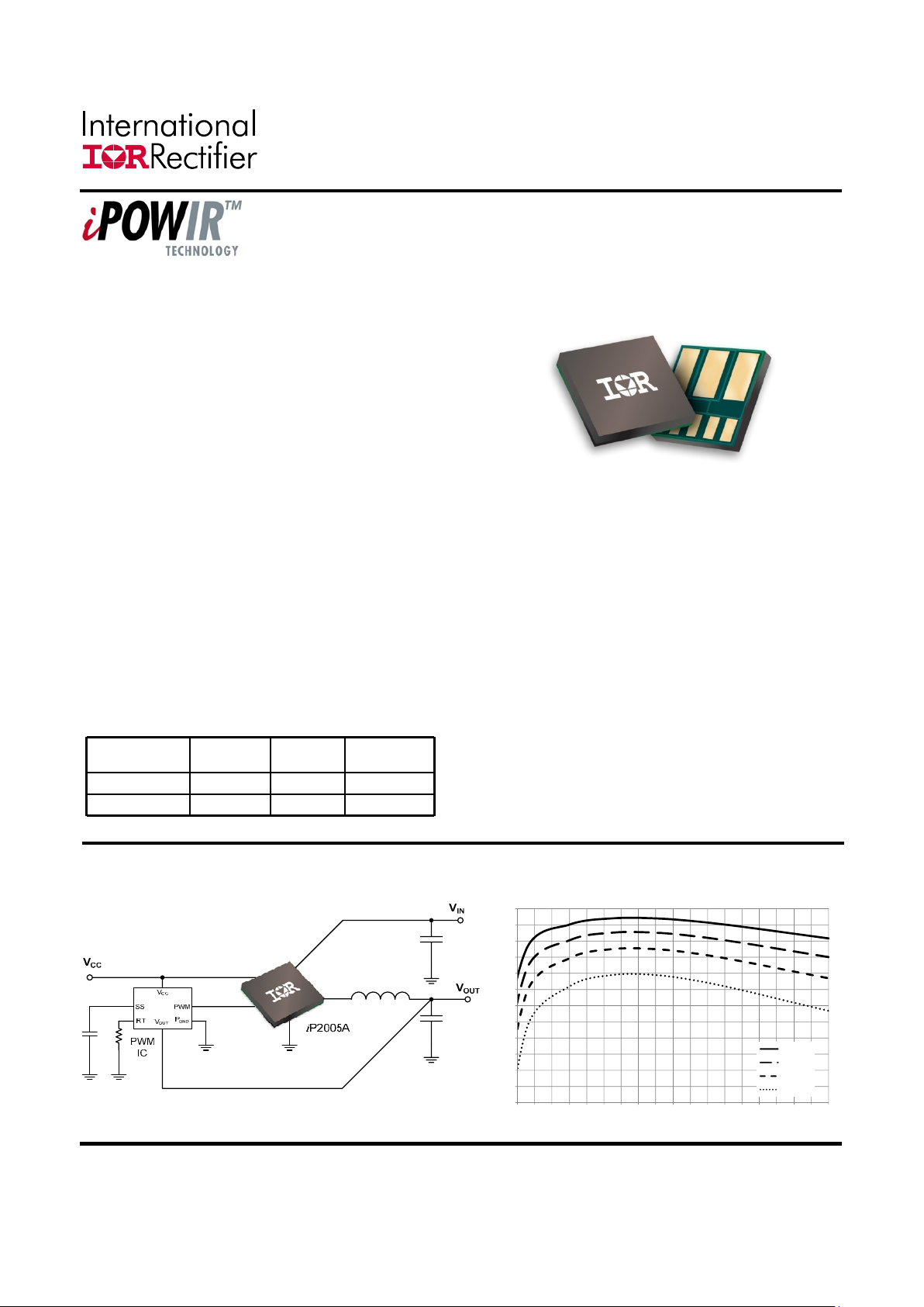
Typical Application
1
iP2005A Product Efficiency
VIN= 12V, FSW= 1MHz, & T
BLK
= 125ºC
70
72
74
76
78
80
82
84
86
88
90
92
94
4 6 8 10121416182022242628303234363840
Effici ency ( % )
Output Current (A)
Vo=3.3V
Vo=2.5V
Vo=1.8V
Vo=1.3V
Page 2
PD-60325
iP2005APbF
VINto P
GND
…………………………..…..-0.5V to 16.5V
V
DD
to P
GND
………………….…….…….-0.5V to 7.5V
CV
CC
to P
GND
……..….……..…………...-0.5V to 7.5V
PWM to P
GND
…………………….………-0.5V to VDD + 0.5V (Note 1)
ENABLE to P
GND
……………..…………-0.5V to VDD + 0.5V (Note 1)
Storage Temperature …………………..-60ºC to 150ºC
Block Temperature ………….………….-40ºC to 150ºC (Note 2)
ESD Rating……………………………....JEDEC, JESD22-A114 (HBM[4KV], Class 3A)
………………………………..JEDEC, JESD22-A115 (MM[400V], Class C)
MSL Rating………………………..……..3
Reflow Temperature …..………………..260ºC Peak
ABSOLUTE MAXIMUM RATINGS
(Voltages referenced to P
GND
)
CAUTION: Stresses above those listed in “Absolute Maximum Ratings” may cause
permanent damage to the device. This is a stress only rating and operation of the
device at these or any other conditions above those listed in the “Recommended
Operating Conditions” section of this specification is not implied.
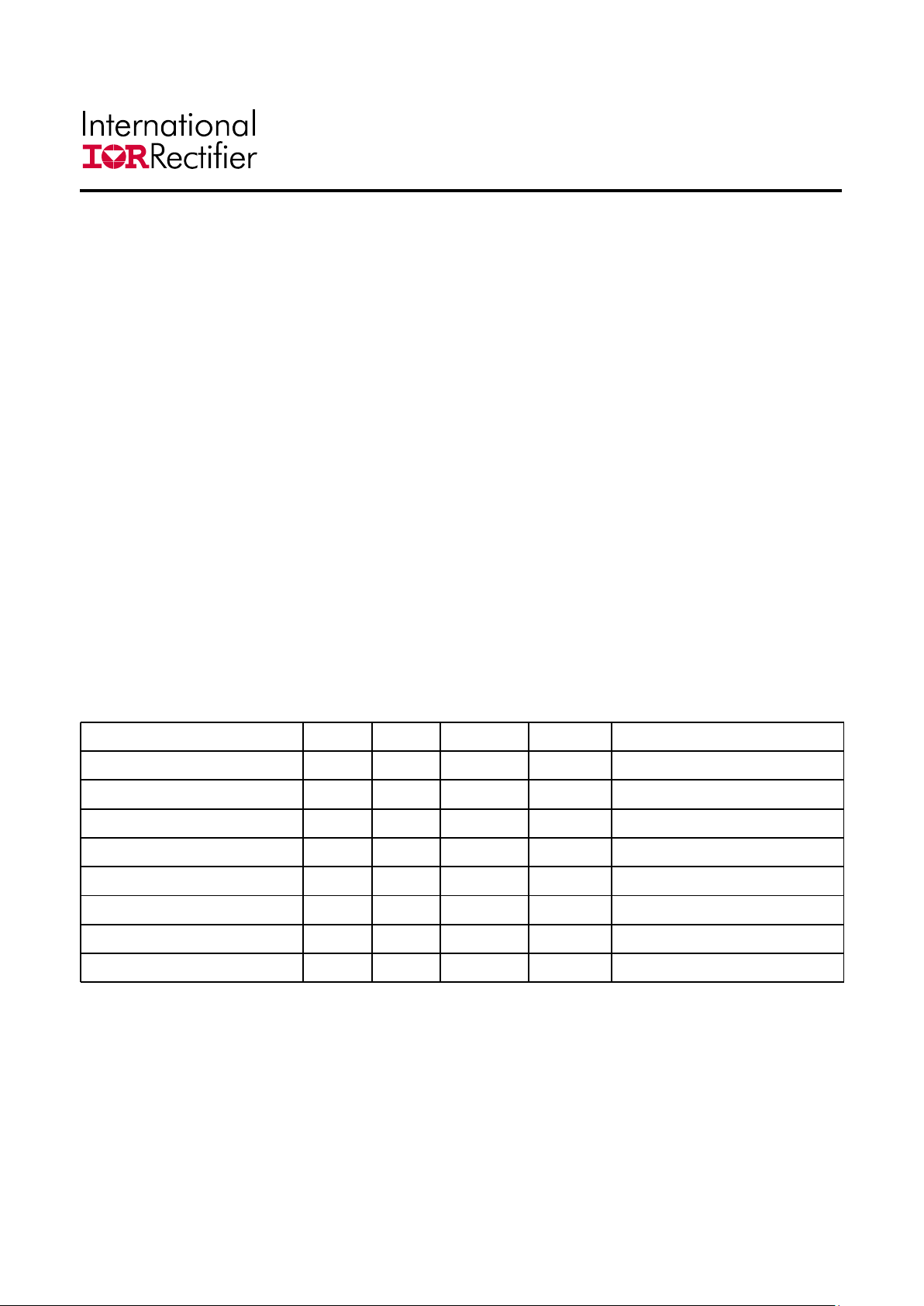
Recommended Operating Conditions
PARAMETER MIN TYP MAX UNITS CONDITIONS
Supply Voltage (V
DD
) 4.5 - 7.0 V
Input Voltage (V
IN
) 6.5 - 13.2 V
Output Voltage (V
OUT
)--5.5V
Output Current (I
OUT
)--40A
Switching Frequency 250 - 1500 kHz
On Time Duty Cycle - - 85 %
Minimum V
SW
On Time 60 - - ns VDD= 5.0V, VIN= 12V
Block Temperature (T
BLK
) -40 - 125 ºC (Note 2)
www.irf.com 2/8/2008
2
Page 3
PD-60325
iP2005APbF
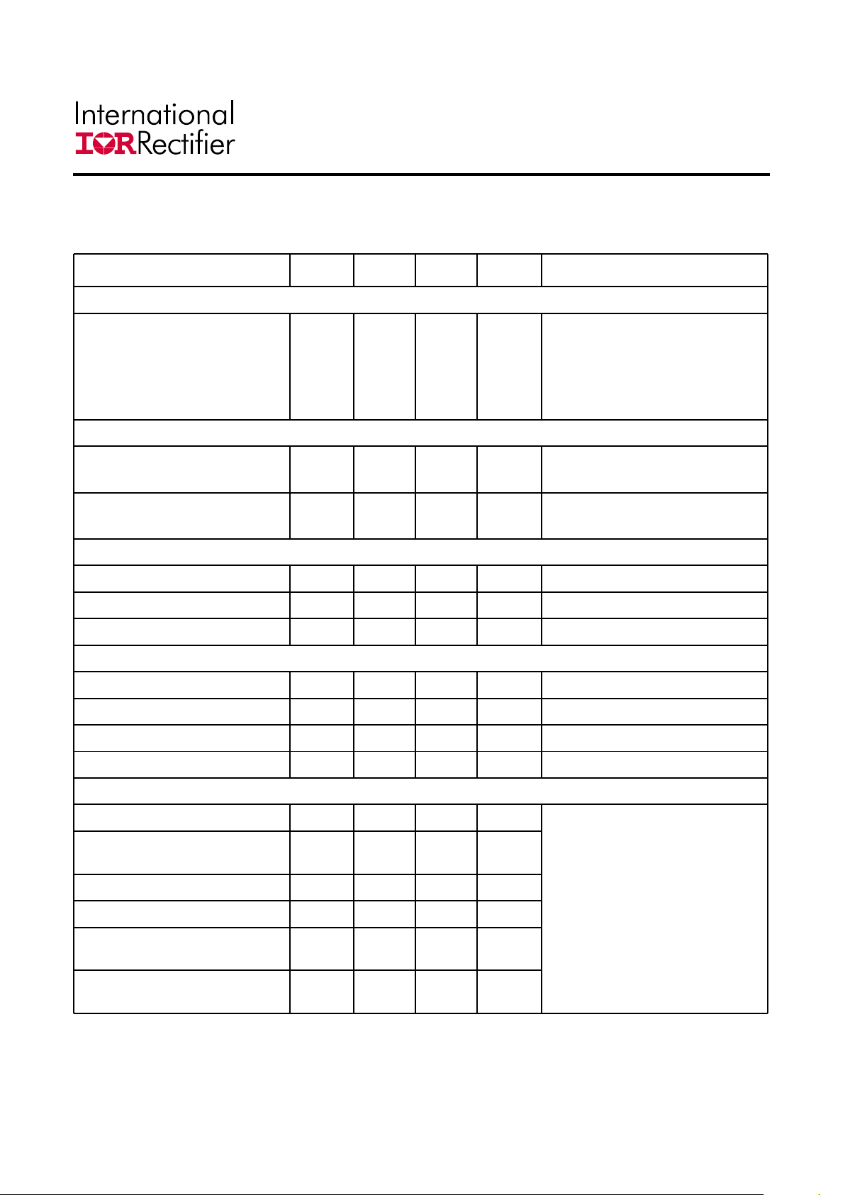
Electrical Specifications
These specifications apply for T
BLK
= 0ºC to 125ºC and VDD= 5.0V unless otherwise specified.
PARAMETER MIN TYP MAX UNITS CONDITIONS
P
LOSS
Power Block Losses - 9.3 11.1 W
V
IN
= 12V, VDD= 5.0V,
V
OUT
= 1.3V, I
OUT
= 40A,
F
SW
= 1MHz,
L
OUT
= 0.3uH, T
BLK
= 25ºC
(Note 3)
V
DD
Supply Current (Stand By)
(I
Q-VDD
)
-2.23mA V
DD
= 5.0, ENABLE = 0V
Supply Current (Operating) - 50 65 mA
V
IN
= 12V, ENABLE = VDD= 5V,
F
SW
= 1MHz, 10% DC
CV
CC
(LDO Output)
Output Voltage 5.5 6.0 6.75 V
Output Current 80 - - mA
Output Capacitor 1.0 - - µF Ceramic, X5R, 16V
Power-On Reset (POR)
V
DD
Rising 3.7 4.1 4.5 V
Hysteresis 140 185 230 mV V
DD
Rising & Falling
CVCC Rising 4.2 4.6 5.0 V
Hysteresis 165 220 275 mV CV
CC
Rising & Falling
ENABLE INPUT
Logic Level Low Threshold (V
IL
)- - 0.8 V
Logic Level High Threshold
(V
IH
)
2.0 - - V
Threshold Hysteresis - 100 - mV
Weak Pull-down Impedance - 100 - kΩ
Rising Propagation Delay
(T
PDH
)
-40-ns
Falling Propagation Delay
(T
PDL
)
-75-ns
Schmitt Trigger Input
V
DD
= POR to 7.0V
www.irf.com 2/8/2008
3
Page 4
PD-60325
iP2005APbF
2/8/2008www.irf.com
4
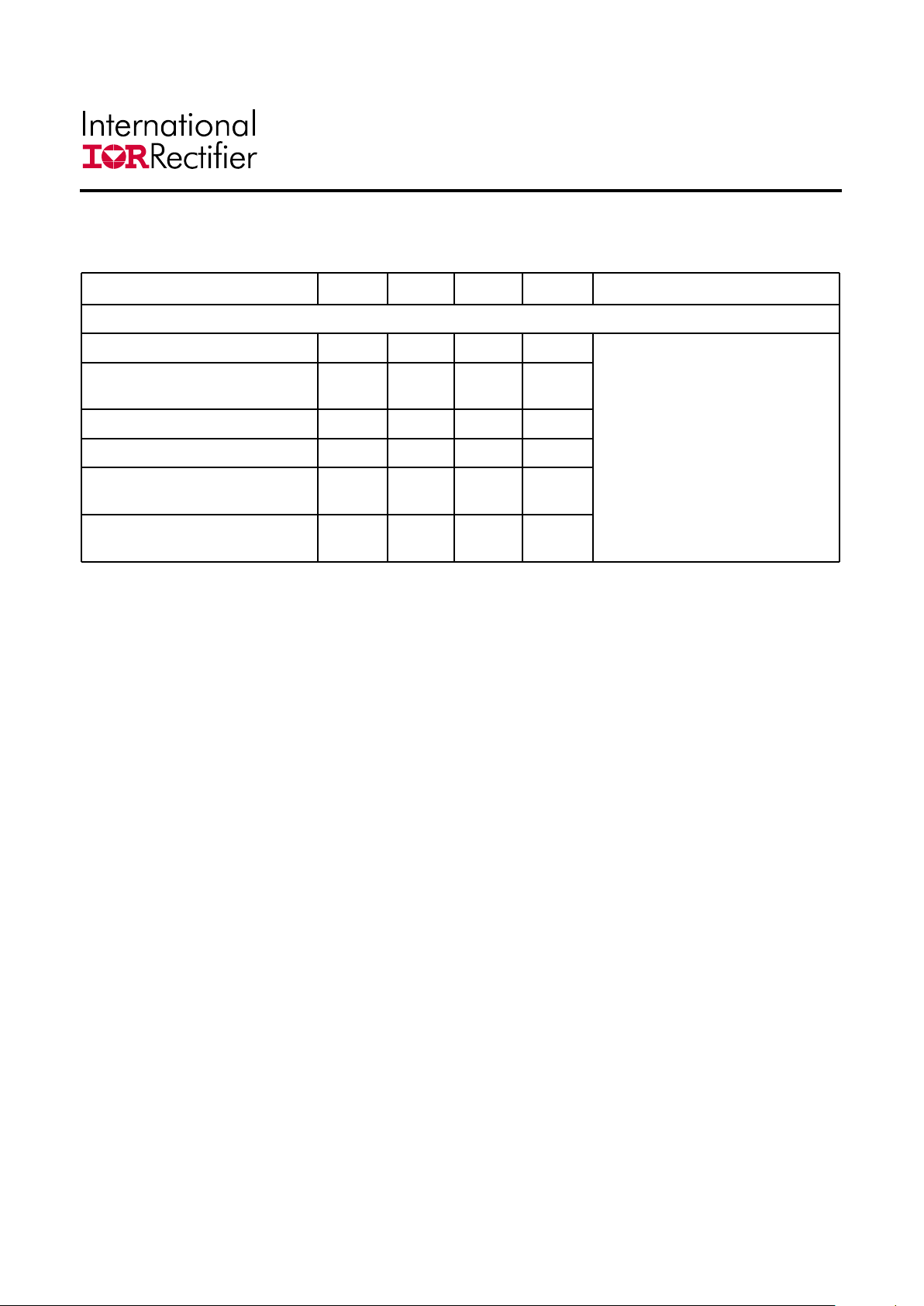
PARAMETER MIN TYP MAX UNITS CONDITIONS
PWM INPUT
Logic Level Low Threshold (V
IL
)- - 0.8 V
Logic Level High Threshold
(V
IH
)
2.0 - - V
Threshold Hysteresis - 100 - mV
Weak Pull-down impedance - 100 - kΩ
Rising Propagation Delay
(T
PDH
)
-60-ns
Falling Propagation Delay
(T
PDL
)
-30-ns
Schmitt Trigger Input
V
DD
= POR to 7.0V
(Note 4)
Electrical Specifications (continued)
These specifications apply for T
BLK
= 0ºC to 125ºC and VDD= 5.0V unless otherwise specified.
Notes:
1. Must not exceed 7.5V
2. Block Temperature (T
BLK
) is defined as any Die temperature within the package
3. Measurement made with six 10µF (TDK C3225X5R1C106KT or equivalent) ceramic capacitors placed across VIN to
PGND pins (see Figure 8)
4. Not associated with rise and fall times. Does not affect Power Loss
Page 5
PD-60325
iP2005APbF
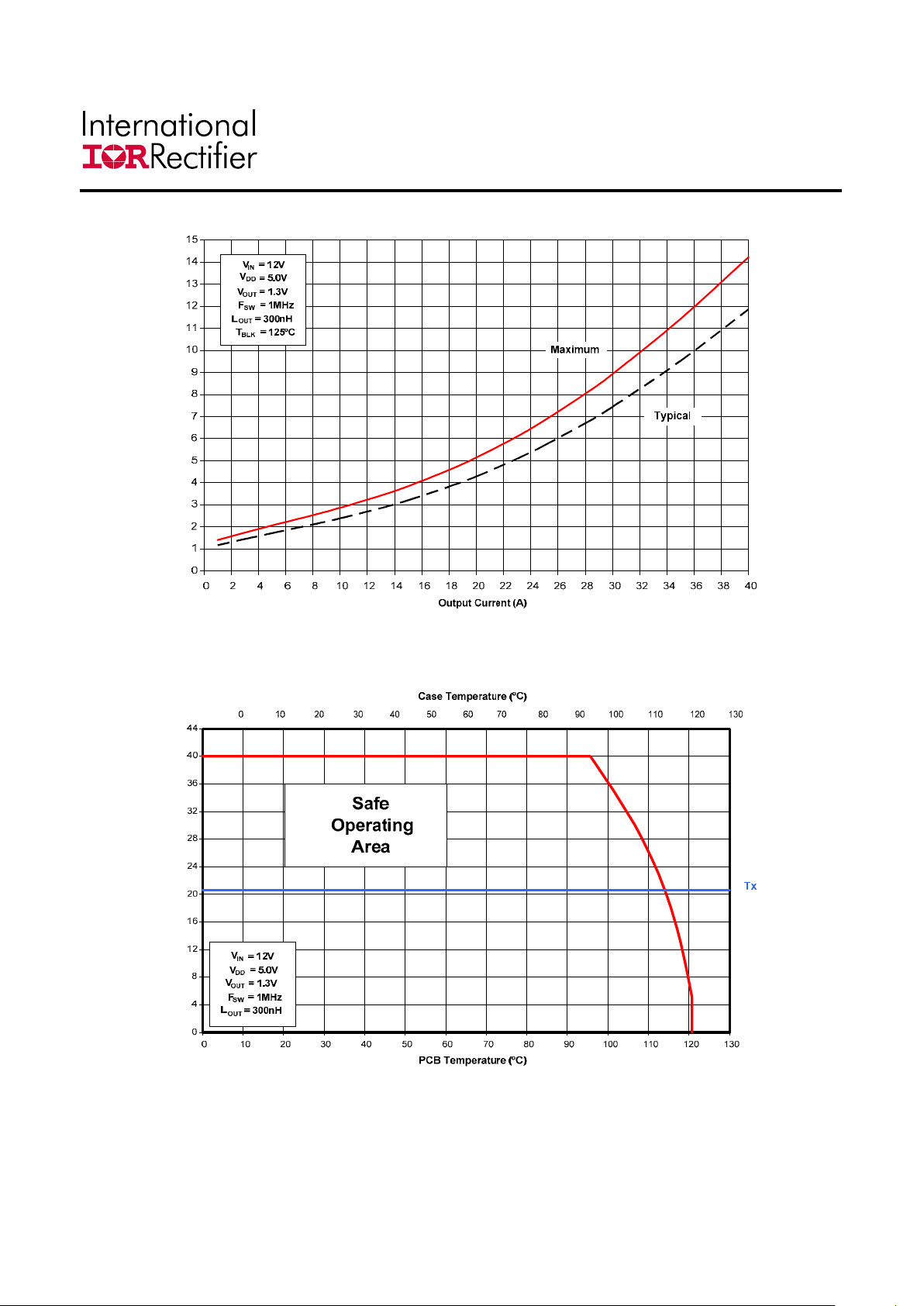
Power Loss Curve
Figure 1 Power Loss Curve
Power Loss (W)
SOA Curve
Figure 2 Safe Operating Area Curve
Output Current (A)
www.irf.com 2/8/2008
5
Page 6
PD-60325
iP2005APbF
Typical Performance Curves
2/8/2008www.irf.com
6
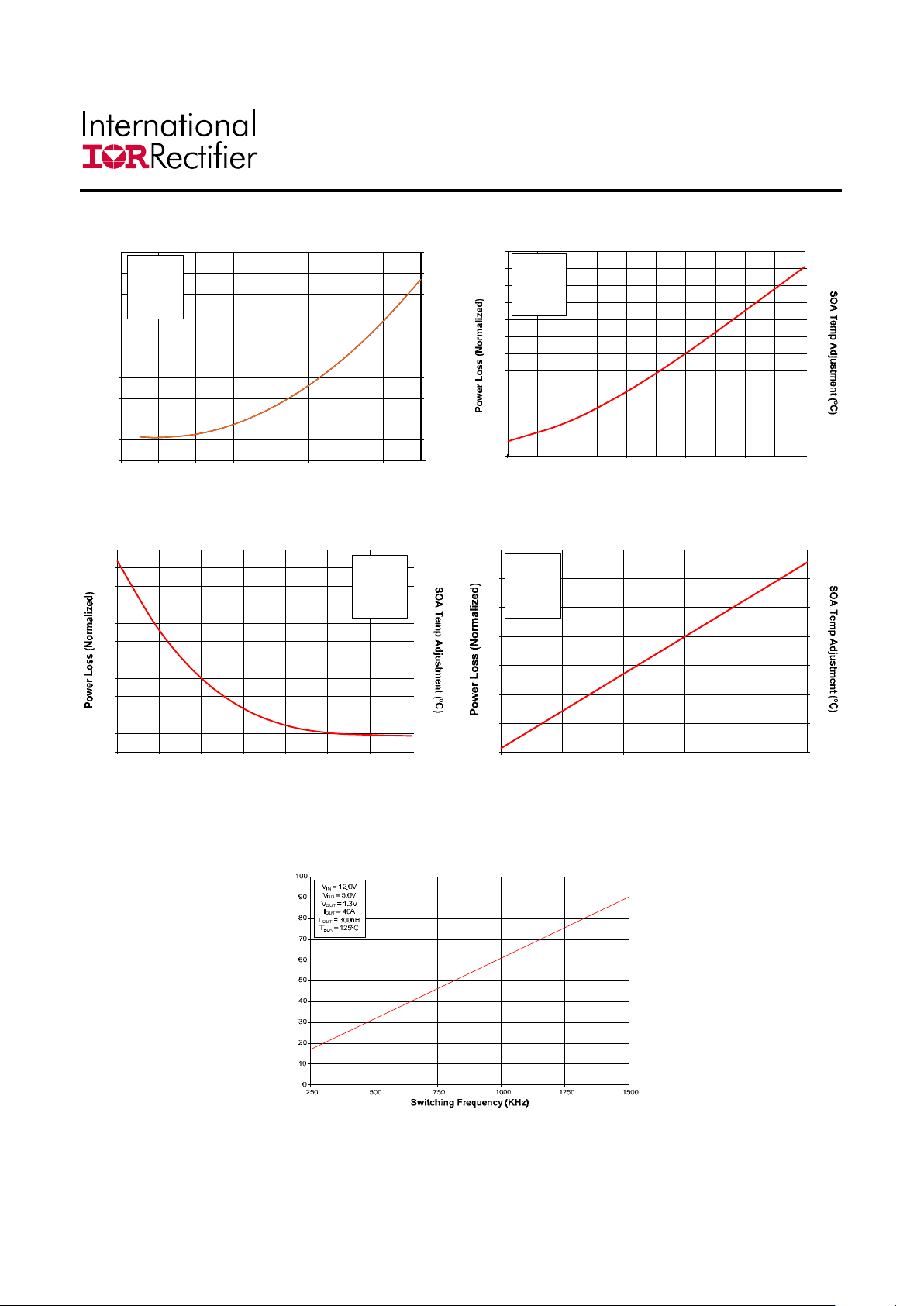
Figure 3 Normalized Power Loss vs. Input Voltage
Power Loss (Normalized)
Figure 4 Normalized Power Loss vs. Output Voltage
0.96
0.98
1.00
1.02
1.04
1.06
1.08
1.10
1.12
1.14
1.16
1.18
1.20
0.8
1.3 1.8 2.3 2.8 3.3
Output Voltage (V)
-0.9
-0.5
0.0
0.5
0.9
1.4
1.9
2.3
2.8
3.3
3.7
4.2
VIN= 12.0V
V
DD
= 5.0V
I
OUT
= 40A
F
SW
= 1MHz
L
OUT
= 300nH
T
BLK
= 125ºC
0.90
0.92
0.94
0.96
0.98
1.00
1.02
1.04
1.06
1.08
1.10
6 7 8 9 10 11 12 13 14
Input Voltage (V)
-2.4
-1.9
-1.4
-1.0
-0.5
0.0
0.5
1.0
1.4
1.9
2.4
SOA Temp Adjustment (ºC)
VDD= 5.0V
V
OUT
= 1.3V
I
OUT
= 40A
F
SW
= 1MHz
L
OUT
= 300nH
T
BLK
= 125ºC
Figure 5 Normalized Power Loss vs. Inductance
Figure 6 Normalized Power Loss vs. Switching Frequency
0.6
0.7
0.8
0.9
1.0
1.1
1.2
1.3
250 500 750 1000 1250 1500
Switching Frequency (kHz)
-10.0
-7.5
-5.0
-2.5
0.0
2.5
5.0
7.5
VIN= 12.0V
V
DD
= 5.0V
V
OUT
= 1.3V
I
OUT
= 40A
L
OUT
= 300nH
T
BLK
= 125ºC
0.96
0.97
0.98
0.99
1.00
1.01
1.02
1.03
1.04
1.05
1.06
1.07
0.1
0.2 0.3 0.4 0.5 0.6 0.7 0.8
Output Inductance (µH)
-1.0
-0.7
-0.5
-0.2
0.0
0.2
0.5
0.7
1.0
1.2
1.4
1.7
VIN= 12.0V
V
DD
= 5.0V
V
OUT
= 1.3V
I
OUT
= 40A
F
SW
= 1MHz
T
BLK
= 125ºC
Figure 7 V
DD
Supply Current vs. Switching Frequency
Average I
DD
(mA)
Page 7
PD-60325
iP2005APbF
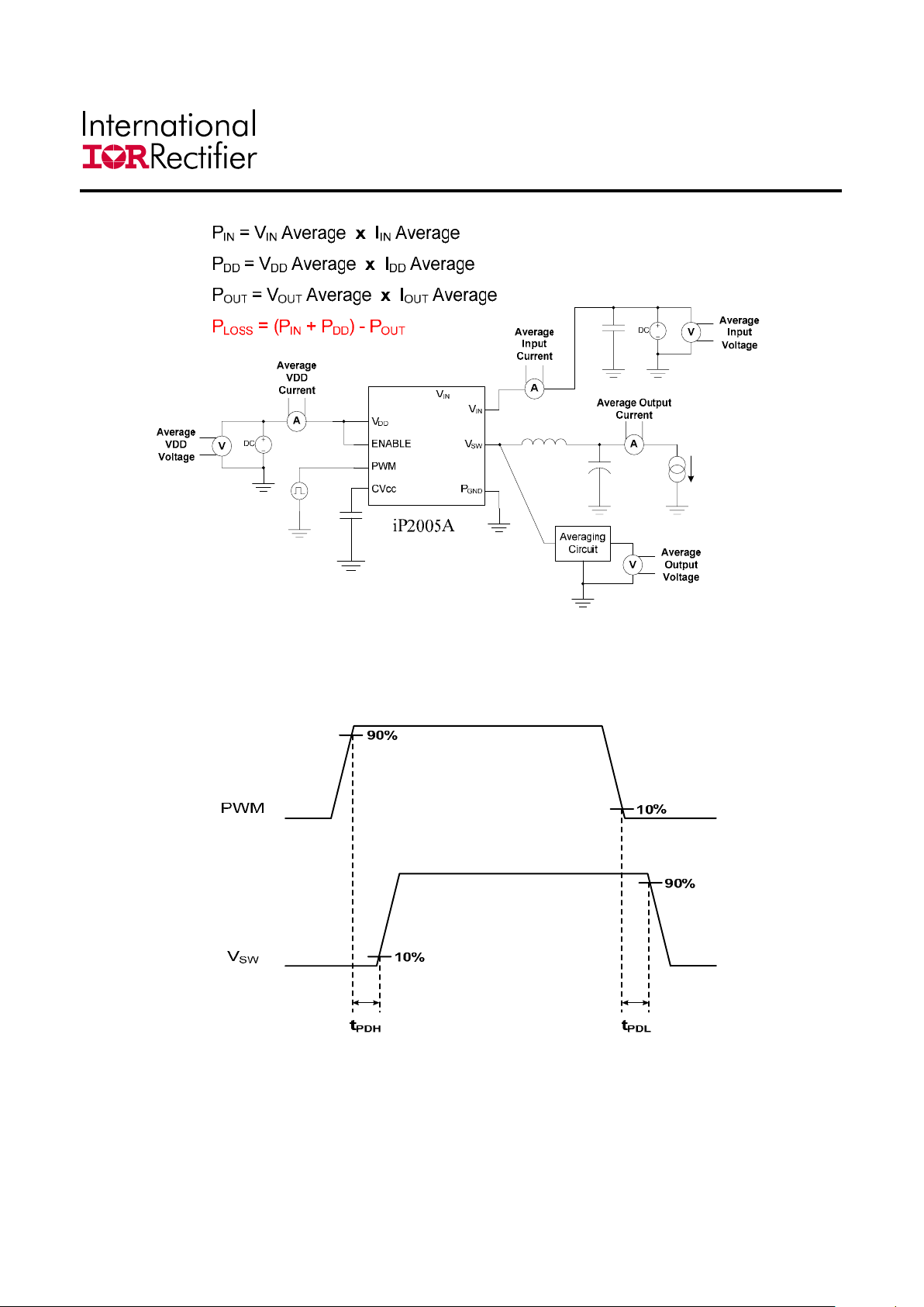
Figure 8 Power Loss Test Circuit
Figure 9 Timing Diagram
www.irf.com 2/8/2008
7
Page 8
PD-60325
iP2005APbF
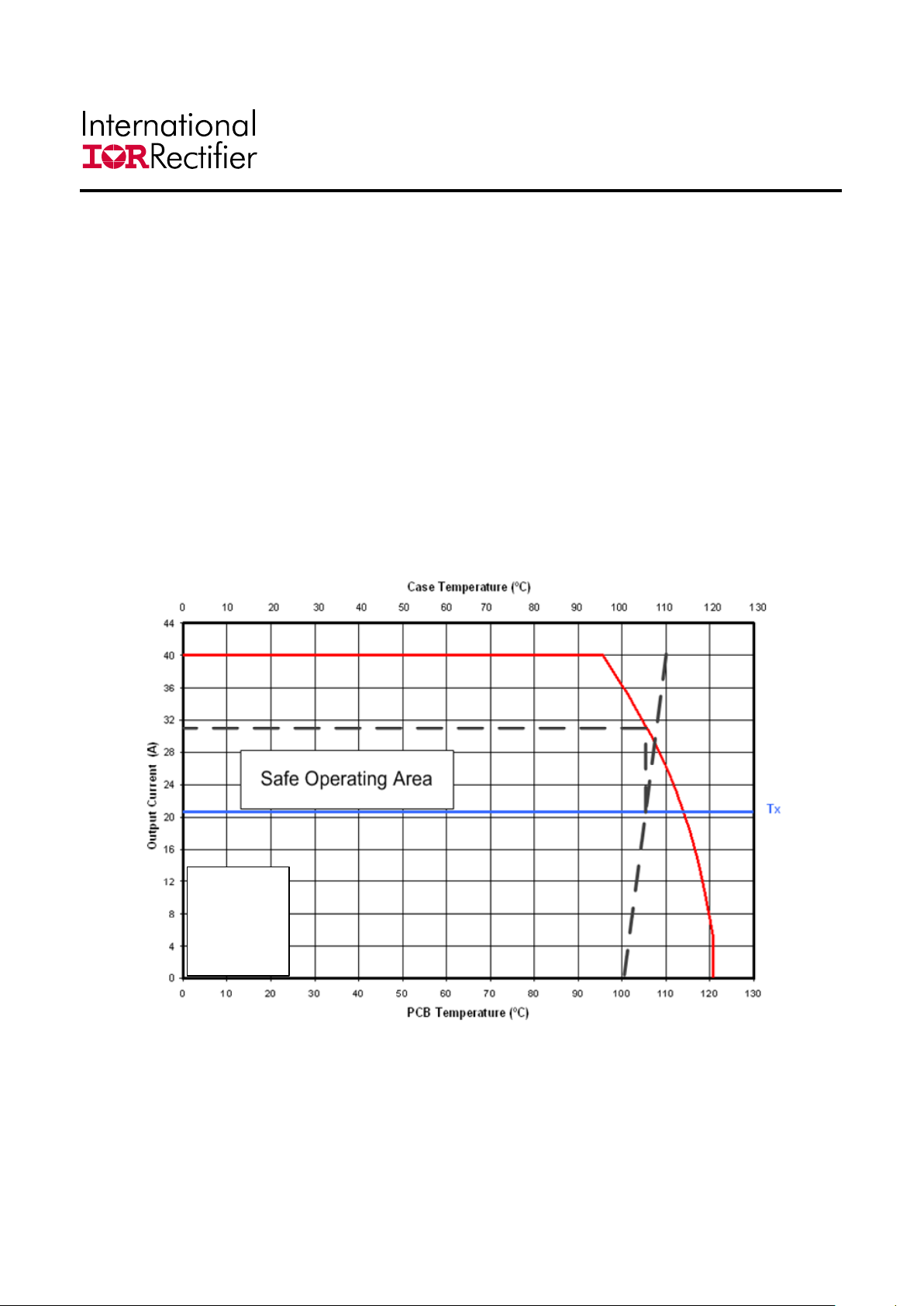
Applying the Safe Operating Area (SOA) Curve
The SOA graph incorporates power loss and thermal resistance information in a way that
allows one to solve for maximum current capability in a simplified graphical manner. It
incorporates the ability to solve thermal problems where heat is drawn out through the
printed circuit board and the top of the case. Please refer to International Rectifier
Application Note AN1047 for further details on using this SOA curve in your thermal
environment.
Procedure
1.Calculate (based on estimated Power Loss) or measure the Case temperature on the
device and the Board temperature near the device (1mm from the edge).
2.Draw a line from Case Temperature axis to the PCB Temperature axis.
3.Draw a vertical line from the T
X
axis intercept to the SOA curve.
4.Draw a horizontal line from the intersection of the vertical line with the SOA curve to the Y-
axis (Output Current). The point at which the horizontal line meets the Y-axis is the SOA
continuous current.
VIN= 12.0V
V
DD
= 5.0V
V
OUT
= 1.3V
F
SW
= 1MHz
L
OUT
= 300nH
Figure 10 SOA Example, Continuous current ≈ 31A for T
PCB
= 100ºC & T
CASE
= 110ºC
www.irf.com 2/8/2008
8
Page 9

PD-60325
iP2005APbF
Calculating Power Loss and SOA for Different Operating Conditions
To calculate Power Loss for a given set of operation conditions, the following procedure
should be followed:
Power Loss Procedure
1.Determine the maximum current for each iP2005A and obtain the maximum power loss
from Figure 1
2.Use the normalized curves to obtain power loss values that match the operating conditions
in the application
3.The maximum power loss under the application conditions is then the product of the power
loss from Figure 1 and the normalized values.
To calculate the Safe Operating Area (SOA) for a given set of operating conditions,
the following procedure should be followed:
SOA Procedure
1.Determine the maximum PCB and CASE temperature at the maximum operating current
for each iP2005A
2.Use the normalized curves to obtain SOA temperature adjustments that match the
operating conditions in the application
3.Then, add the sum of the SOA temperature adjustments to the TXaxis intercept in Figure
2
Design Example
Operating Conditions:
Output Current = 30A Input Voltage = 10V Output Voltage = 1.3V
Switching Freq = 750kHz Inductor = 0.2µH Drive Voltage (V
DD
) = 5V
Calculating Maximum Power Loss:
(Figure 1) Maximum power loss = 9.0W
(Figure 3) Normalized power loss for input voltage ≈ 0.95
(Figure 4) Normalized power loss for output voltage ≈ 1.0
(Figure 5) Normalized power loss for output inductor ≈ 1.026
(Figure 6) Normalized power loss for switch frequency ≈ 0.87
Calculated Maximum Power Loss ≈ 9.0W x 0.95 x 1.0 x 1.026 x 0.87 ≈ 7.63W
www.irf.com 2/8/2008
9
Page 10
PD-60325
iP2005APbF
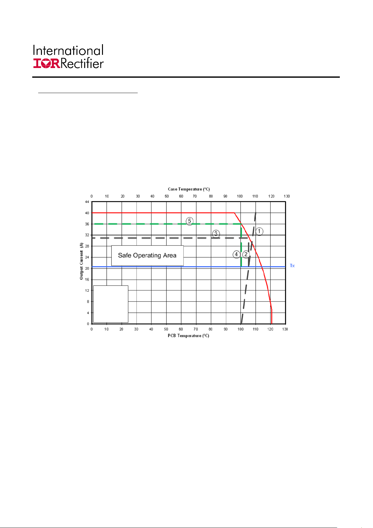
Calculating SOA Temperature:
(Figure 3) SOA temperature adjustment for input voltage ≈ -1.2ºC
(Figure 4) SOA temperature adjustment for output voltage ≈ 0.0ºC
(Figure 5) SOA temperature adjustment for output inductor ≈ 0.6 ºC
(Figure 6) SOA temperature adjustment for switch frequency ≈ -3.5 ºC
T
X
axis intercept adjustment ≈ -1.2 ºC + 0.0 ºC + 0.6 ºC – 3.5 ºC ≈ -4.1 ºC
Assuming T
PCB
= 100ºC & T
CASE
= 110ºC
The following example shows how the SOA current is adjusted for T
X
decrease of 4.1ºC
VIN= 12.0V
V
DD
= 5.0V
V
OUT
= 1.3V
F
SW
= 1MHz
L
OUT
= 300nH
1. Draw a line from Case Temperature axis to the PCB Temperature axis.
2. Draw a vertical line from the T
X
axis intercept to the SOA curve.
3. Draw a horizontal line from the intersection of the vertical line with the SOA curve to the
Y-axis (Output Current). The point at which the horizontal line meets the Y-axis is the
SOA continuous current.
4. Draw a new vertical line from the T
X
axis by adding or subtracting the SOA adjustment
temperature from the original T
X
intercept point.
5. Draw a horizontal line from the intersection of the new vertical line with the SOA curve to
the Y-axis (Output Current). The point at which the horizontal line meets the Y-axis is
the new SOA continuous current.
The SOA adjustment indicates the part is still allowed to run at a continuous current of 36A.
www.irf.com 2/8/2008
10
Page 11
2/8/2008www.irf.com
11
PD-60325
iP2005APbF
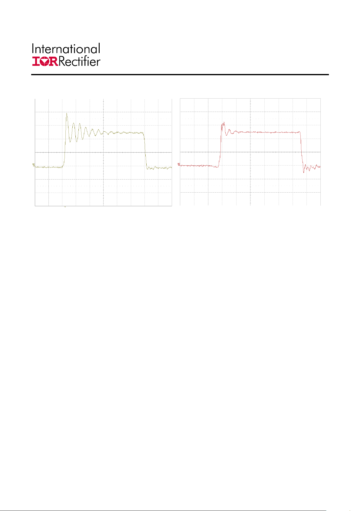
Optimized EMI Feature
5V/div
20nS/div
5V/div
20nS/div
Vsw of iP2005A
Vsw of iP2003A
The iP2005A is designed for low Electromagnetic Interference (EMI) which minimizes power
loss and space, and simplifies system design by eliminating the need for external snubber
circuits. These benefits are achieved by optimizing the internal component layout, integrating
bypass filters and implementing active clamp circuitry as a means of reducing switching node
voltage ringing; which is one of main sources of EMI. The figures above show waveform
comparisons of switching node voltages of the previous generation iP2003A product and
iP2005A under equivalent operation conditions.
Page 12
PD-60325
iP2005APbF
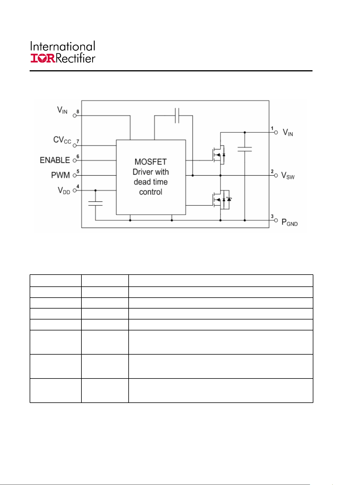
Internal Block Diagram
Figure 11 Internal Block Diagram
Pin Description
Pin Number Pin Name Description
1, 8 V
IN
Input voltage pin. Connect input capacitors close to this pin.
2 Vsw Voltage Switching Node – pin connection to the output inductor.
3P
GND
Power Ground
4V
DD
Supply voltage to internal circuitry.
5PWM
TTL level input to MOSFET drivers. When PWM is HIGH, the Control
FET is on and the Sync FET is off. When PWM is LOW, the Sync FET
is on and the Control FET is off.
6 ENABLE
When set to logic level high, internal circuitry of the device is enabled.
When set to logic level low, the Control and Synchronous FETs are
turned off.
7CV
CC
Output of internal regulator. Attached a minimum of 1.0µF capacitance
from this pin to PGND. Recommended to use 16V, X5R, Ceramic type
capacitor.
www.irf.com 2/8/2008
12
Page 13
PD-60325
iP2005APbF
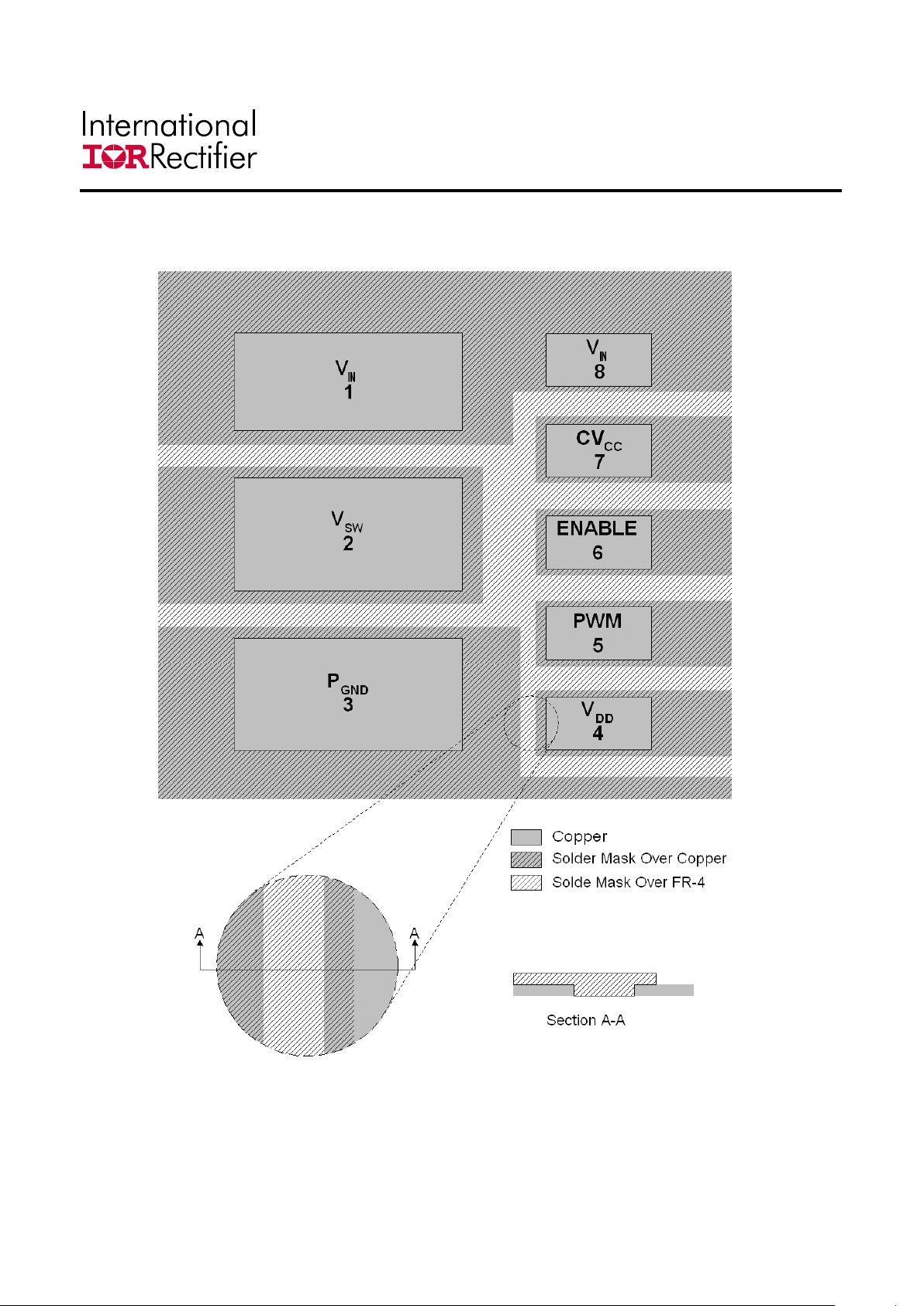
Recommended PCB Layout
Figure 12 Top copper and Solder-mask layer of PCB layout
www.irf.com 2/8/2008
13
Page 14
PD-60325
iP2005APbF
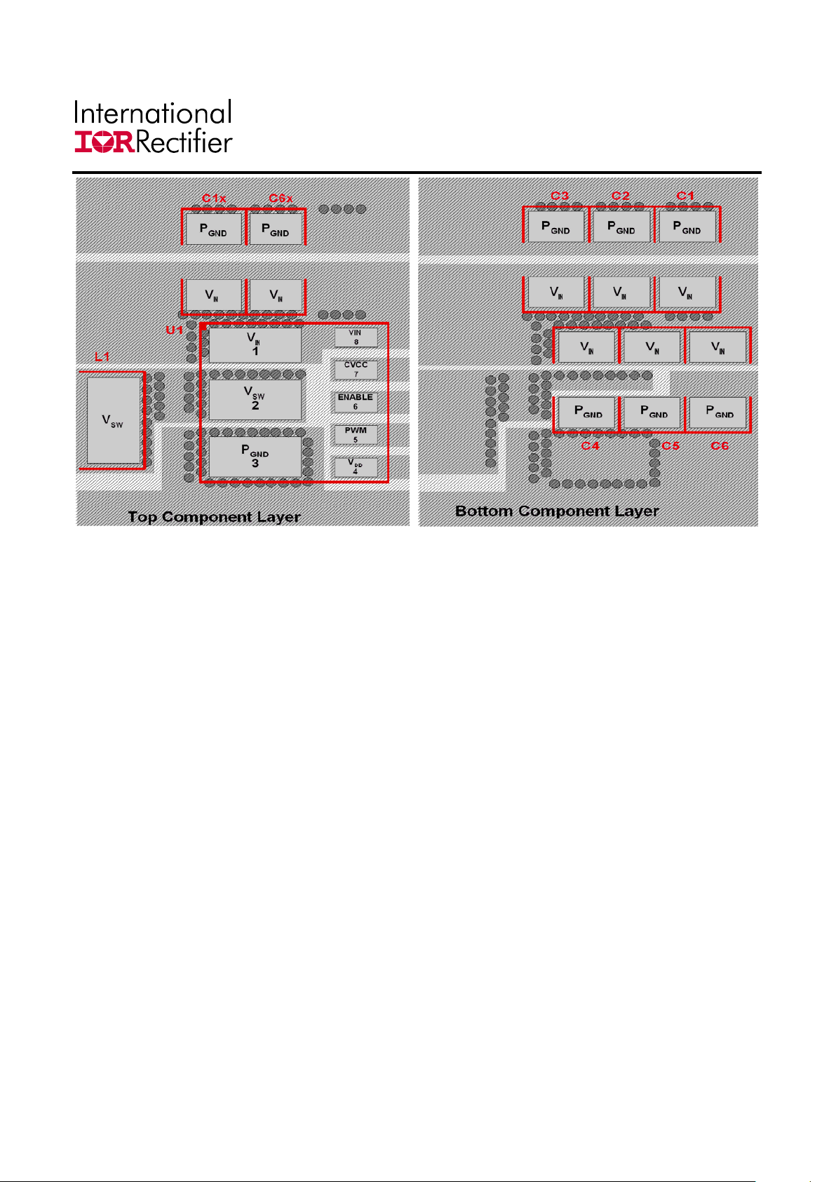
Figure 13 Top & Bottom Component and Via Placement (Topside, Transpar ent view down)
PCB Layout Guidelines
The following guidelines are recommended to reduce the parasitic values and optimize
overall performance.
• All pads on the iP2005A footprint design need to be Solder-mask defined (see Figure 12) .
Also refer to International Rectifier application notes AN1028 and AN1029 for further
footprint design guidance.
• Place as many vias around the Power pads (V
IN
, VSW, and P
GND
) for both electrical and
optimal thermal performance.
• A minimum of six 10µF, X5R, 16V ceramic capacitors per iP2005A are needed for greater
than 30A operation. This will result in the lowest loss due to input capacitor ESR.
• Placement of the ceramic input capacitors is critical to optimize switching performance. In
cases where there is a heatsink on the case of iP2005A, place all six ceramic capacitors
right underneath the iP2005A footprint (see Figure 13 Bottom Component Layer). In
cases where there is not heatsink, C1 and C6 on the bottom layer may be moved to the
C1x and C6x locations (respectively) on the top component layer (see Figure 13 Top
Component Layer). In both cases, C2 – C5 need to be placed right underneath the
iP2005A PCB footprint.
• Dedicate at least two layer to for P
GND
only
• Duplicate the Power Nodes on multiple layers (refer to AN1029).
www.irf.com 2/8/2008
14
Page 15
PD-60325
iP2005APbF
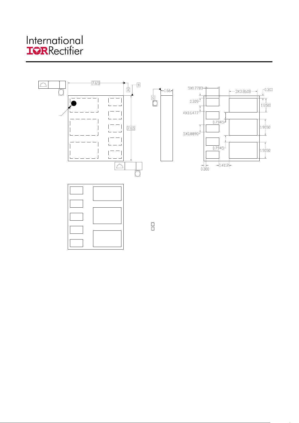
Mechanical Outline Drawing
ELECTRICAL I/O
BOTTOM VIEW
0.10
C
2X
TOP VIEW
5
4
SIDE VIEW BOTTOM VIEW
CORNER ID
0.10
C
2X
5
Notes:
1. Dimensions & Tolerances per ASME Y14.5M –1994
2. Dimensions are shown in Millimeters
3. Tolerances are:
.XX = +/- 0.1
.XXX = +/- 0.025
.XXXX = +/- 0.01
Primary datum C is seating plane
Bilateral tolerance zone is applied to each side of package body
Layout Notes:
1. Land patterns on user’s PCB should be an identical mirror
image of the pattern shown in bottom view
2. Lands should be solder mask defined
3. All I/O pads on this product are metal finish with flash gold
ENABLE
6
CV
CC
7
V
IN
8
V
IN
1
V
SW
2
P
GND
3
V
DD
4
PWM
5
4
5
Figure 14 Mechanical Outline Drawing
www.irf.com 2/8/2008
15
Page 16
PD-60325
iP2005APbF
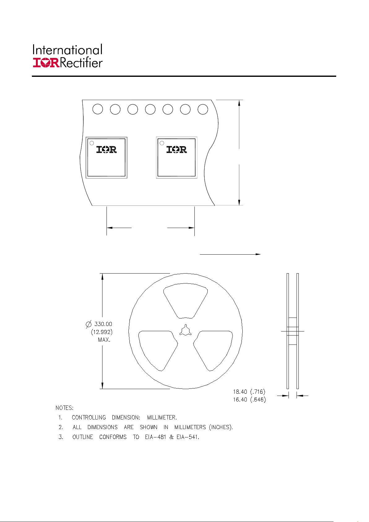
Tape and Reel Information
FEED DIRECTION
12.00 (.473)
2005AP
XXXX
YYMM
16.00 (.630)
2005AP
XXXX
YYMM
XXXX
Figure 15 Tape and Reel Information
www.irf.com 2/8/2008
16
Page 17
PD-60325
iP2005APbF
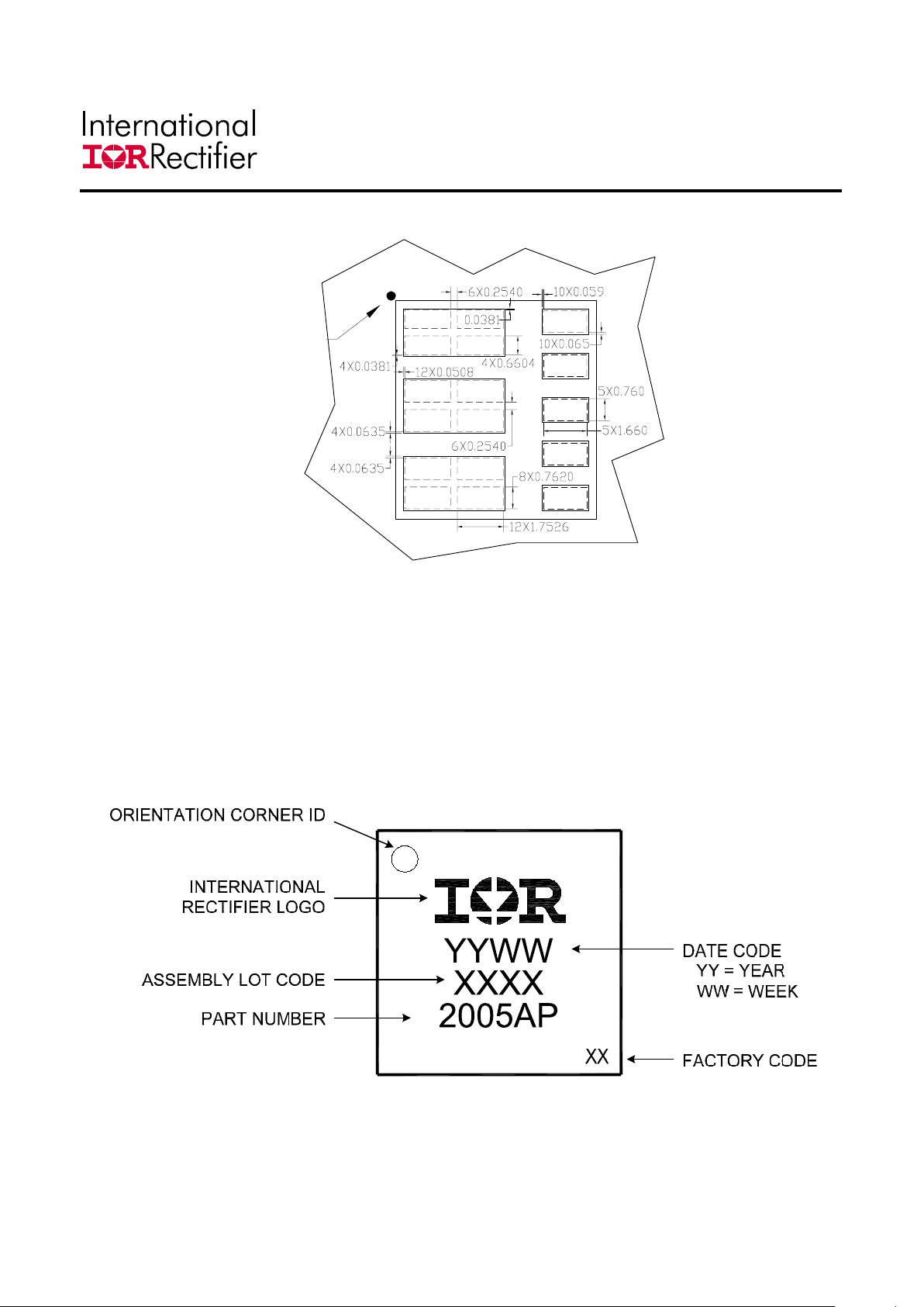
Recommended Solder Paste Stencil Design
Notes:
1.This view is stencil squeegee view
2.Dimensions are shown in millimeters
3.This opening is based on using 150 micron thick stencil. If using a different thickness stencil, this opening needs to be
adjusted accordingly.
4.Dashed lines show stencil openings. Solid lines show PCB pad openings.
5.The recommended reflow peak temperature is 260ºC. The total furnace time is approximately 5 minutes with
approximately 10 seconds at peak temperature.
CORNER ID
Figure 16 Solder Paste Stencil Design
Part Marking
Figure 17 Part Marking
www.irf.com 2/8/2008
17
Page 18

PD-60325
iP2005APbF
IR WORLD HEADQUARTERS: 101 N. Sepulveda Blvd., El Segundo, California 90245, USA Tel: (310) 252-7105
TAC Fax: (310) 252-7903
This product has been designed for the Industrial market.
Visit us at www.irf.com for sales contact information
Data and specifications subject to change without notice. 12/24/2007
www.irf.com 2/8/2008
18
 Loading...