

Page 1
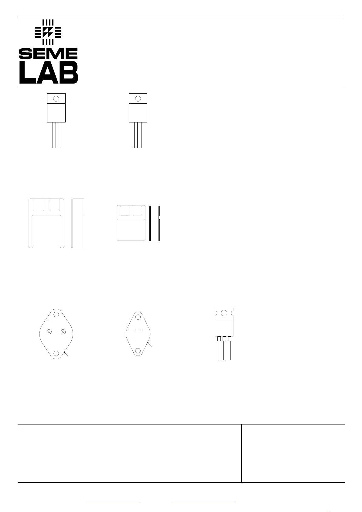
Pin 1 – ADJ.
Pin 2 – V
OUT
Pin 3 – V
IN
SMD1
CERAMIC SURFACE
MOUNT
Pin 1 – ADJ.
Pin 2 – V
OUT
Pin 3 – V
IN
Case – V
OUT
G Package – TO257
Pin 1 – ADJ.
Pin 2 – V
IN
Case – V
OUT
K Package – TO3
Pin 1 – ADJ.
Pin 2 – V
IN
Case – V
OUT
R Package – TO66
Prelim. 8/00
Semelab plc. Telephone +44(0)1455 556565. Fax +44(0)1455 552612.
E-mail: sales@semelab.co.uk
Website: http://www.semelab.co.uk
IP117, IP117A
IP317, IP317A
LM117, LM117A
1.5 AMP
POSITIVE ADJUSTABLE
VOLTAGE REGULATOR
FOR HI-REL APPLICATIONS
40V
60V
Internally limited
Internally limited
See Table Above
–65 to 150°C
ABSOLUTE MAXIMUM RATINGS (T
case
= 25°C unless otherwise stated)
FEATURES
• Output voltage range of:
1.25 to 40V for standard version
1.25 to 60V for HV version
• Output voltage tolerance 1%
• Load regulation 0.3%
• Line regulation 0.01%/V
• Complete series of protections:
current limiting
thermal shutdown
soa control
• Also available in TO220 metal
isolated package (1mm pins)
12
3
3
12
Pin 1 – ADJ.
Pin 2 – V
OUT
Pin 3 – V
IN
T Package – TO220 Plastic
123
1
23
Pin 1 – ADJ.
Pin 2 – V
OUT
Pin 3 – V
IN
Case – Isolated
IG Package – TO257
Pin 1 – ADJ.
Pin 2 – V
OUT
Pin 3 – V
IN
SMD05
CERAMIC SURFACE
MOUNT
1
23
!
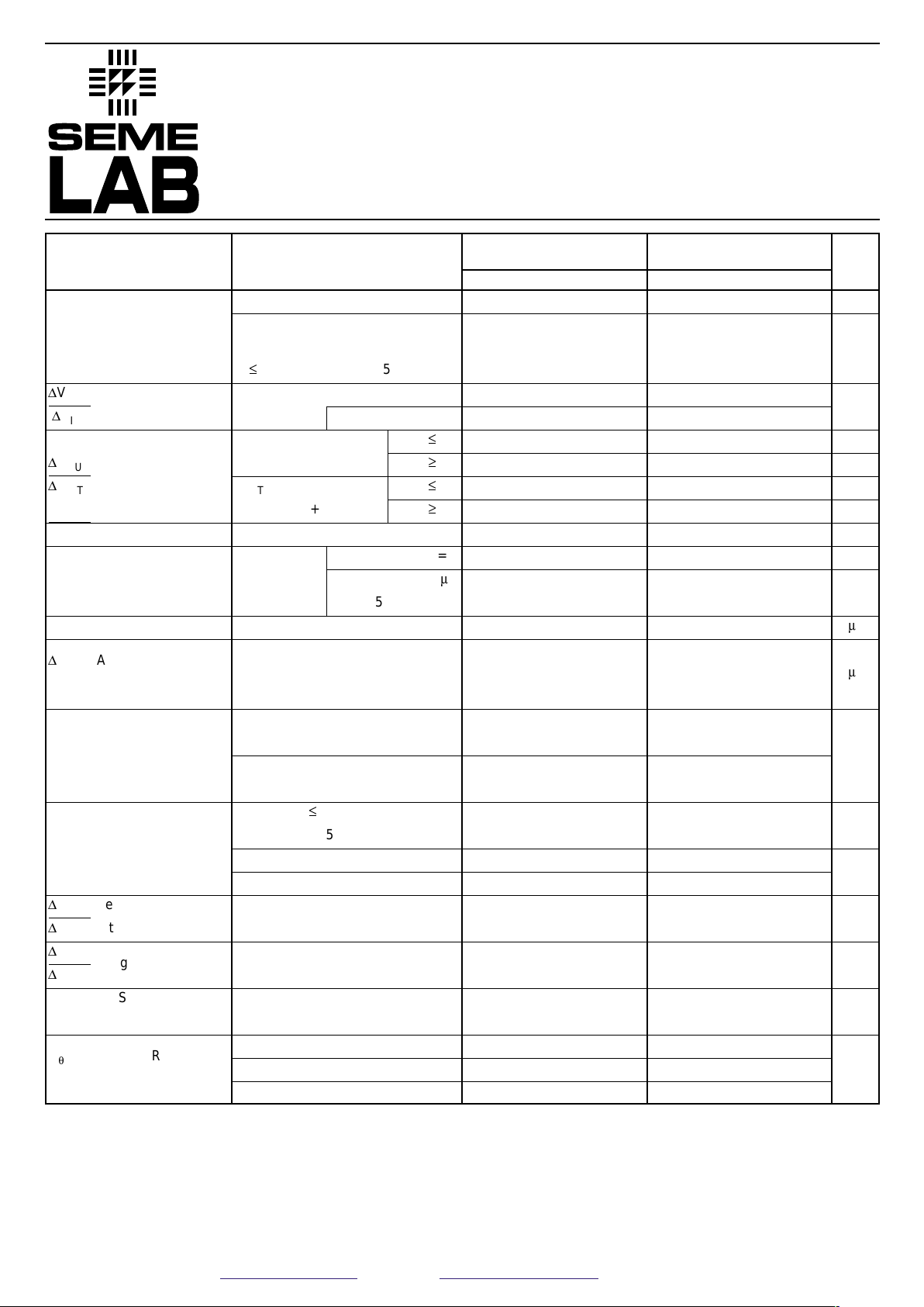
V
I–O
Input - Output Differential Voltage – Standard
– HV Series
I
O
Output Current
P
D
Power Dissipation
T
J
Operating Junction Temperature Range
T
STG
Storage Temperature
!
Page 2
Prelim. 8/00
Semelab plc. Telephone +44(0)1455 556565. Fax +44(0)1455 552612.
E-mail: sales@semelab.co.uk
Website: http://www.semelab.co.uk
IP117, IP117A
IP317, IP317A
LM117, LM117A
1) Regulation is measured at constant junction temperature, using pulse testing at a low duty cycle. Changes in output voltage due to heating effects
are covered under thermal regulation specifications. Load regulation is measured from the bottom of the package for the TO–3 and TO–66 packages, at the junction of the wide and narrow portion of the output lead for the TO–220 package, and 1/8” below the base of the package on the output pin of the TO–257 package.
2) Test Conditions unless othewise stated: VIN– V
OUT
= 5V , TJ= 25°C , I
OUT
= 0.5A , I
MAX
= 1.5A.
P
MAX
= 10W for SMD1, 20W for all other package styles.
V
MAX
= 40V for standard series , 60V for HV series.
1.238 1.25 1.262
1.225 1.250 1.270
0.005 0.010
0.010 0.020
515
0.1 0.3
15 50
0.3 1
0.002 0.020
65
66 80
50 100
0.2 5
3.5 5
3.5 7
1.5 2.2
0.30 0.50
0.10
12
0.3 1
0.001
2.3 3
57
35
1.200 1.250 1.300
0.010 0.020
0.020 0.050
515
0.1 0.3
20 50
0.3 1
0.030 0.070
65
66 80
50 100
0.2 5
3.5 5
3.5 7
1.5 2.2
0.30 0.50
0.10
1
0.3 1
0.001
2.3 3
57
35
IP117A , IP117AHV IP117 , IP117HV
LM117A , LM117AHV LM117 , LM117HV
Parameter Test Conditions Min. Typ. Max. Min. Typ. Max. Units
V
REF
Reference Voltage
D
V
OUT
Line Regulation
1
D
V
IN
D
V
OUT
Load Regulation
1
D
I
OUT
Thermal Regulation
Ripple Rejection
I
ADJ
Adjust Pin Current
D
I
ADJ
Adjust Pin Current
Change
I
MIN
Minimum Load
Current
I
CL
Current Limit
D
V
OUT
Temperature
D
TEMP Stability
D
V
OUT
Long Term Stability
D
TIME
e
n
RMS Output Noise
(% of V
OUT
)
R
q
JC
Thermal Resistance
Junction to Case
I
OUT
= 10mA
I
OUT
= 10mA to I
MAX
VIN– V
OUT
= 3V to V
MAX
P£P
MAX
TJ= –55 to +150°C
V
IN
– V
OUT
= 3V to V
MAX
TJ= –55 to +150°C
I
OUT
= 10mA to I
MAX
V
OUT
£
5V
V
OUT
³
5V
I
OUT
= 10mA to I
MAX
V
OUT
£
5V
T
J
= –55 to +150°C V
OUT
³
5V
t
p
= 20ms
C
ADJ
= 0
V
OUT
= 10V
C
ADJ
= 10mF
f = 120Hz
T
J
= –55 to +150°C
T
J
= –55 to +150°C
I
OUT
= 10mA to I
MAX
TJ= –55 to +150°C
V
IN
– V
OUT
= 2.5V to V
MAX
VIN– V
OUT
= 40V
T
J
= –55 to +150°C
V
IN
– V
OUT
= 60V (HV SERIES)
TJ= –55 to +150°C
V
IN
– V
OUT
£
15V
T
J
= –55 to +150°C
V
IN
– V
OUT
= 40V
V
IN
– V
OUT
= 60V (HV SERIES)
TJ= –55 to +150°C
T
A
= +125°C t = 1000 Hrs
f = 10 Hz to 10 kHz
K Package
R Package
G, IG Packages
V
V
% / V
mV
%
mV
%
%/W
dB
dB
m
A
m
A
mA
A
A
%
%
%
°C/W
Page 3

Prelim. 8/00
Semelab plc. Telephone +44(0)1455 556565. Fax +44(0)1455 552612.
E-mail: sales@semelab.co.uk
Website: http://www.semelab.co.uk
IP117, IP117A
IP317, IP317A
LM117, LM117A
1) Regulation is measured at constant junction temperature, using pulse testing at a low duty cycle. Changes in output voltage due to heating effects
are covered under thermal regulation specifications. Load regulation is measured from the bottom of the package for the TO–3 and TO–66 packages, at the junction of the wide and narrow portion of the output lead for the TO–220 package, and 1/8” below the base of the package on the output pin of the TO–257 package.
2) Test Conditions unless othewise stated: VIN– V
OUT
= 5V , TJ= 25°C , I
OUT
= 0.5A , P
MAX
= 20W , I
MAX
= 1.5A
V
MAX
= 40V for standard series , 60V for HV series.
1.238 1.25 1.262
1.225 1.25 1.270
0.005 0.010
0.010 0.020
525
0.1 0.5
15 50
0.3 1
0.002 0.020
65
66 80
50 100
0.2 5
3.5 10
3.5 12
1.5 2.2
0.15 0.40
0.10
12
0.3 1
0.003
2.3 3
45
1.200 1.250 1.300
0.010 0.040
0.020 0.070
525
0.1 0.5
20 70
0.3 1.5
0.030 0.070
65
66 80
50 100
0.2 5
3.5 10
3.5 12
1.5 2.2
0.15 0.40
0.10
1
0.3 1
0.003
2.3 3
57
IP317A IP317
IP317AHV IP317HV
Parameter Test Conditions Min. Typ. Max. Min. Typ. Max. Units
V
REF
Reference Voltage
D
V
OUT
Line Regulation
1
D
V
IN
D
V
OUT
Load Regulation
1
D
I
OUT
Thermal Regulation
Ripple Rejection
I
ADJ
Adjust Pin Current
D
I
ADJ
Adjust Pin Current
Change
I
MIN
Minimum Load
Current
I
CL
Current Limit
D
V
OUT
Temperature
D
TEMP Stability
D
V
OUT
Long Term Stability
D
TIME
e
n
RMS Output Noise
(% of V
OUT
)
R
q
JC
Thermal Resistance
Junction to Case
I
OUT
= 10mA
I
OUT
= 10mA to I
MAX
VIN– V
OUT
= 3V to V
MAX
P£P
MAX
TJ= 0 to 125°C
V
IN
– V
OUT
= 3V to V
MAX
TJ= 0 to 125°C
I
OUT
= 10mA to I
MAX
V
OUT
£
5V
V
OUT
³
5V
I
OUT
= 10mA to I
MAX
V
OUT
£
5V
T
J
= –55 to +150°C V
OUT
³
5V
t
p
= 20ms
C
ADJ
= 0
V
OUT
= 10V
C
ADJ
= 10mF
f = 120Hz
T
J
= 0 to 125°C
T
J
= 0 to 125°C
I
OUT
= 10mA to I
MAX
TJ= 0 to 125°C
V
IN
– V
OUT
= 2.5V to V
MAX
VIN– V
OUT
= 40V
T
J
= 0 to 125°C
V
IN
– V
OUT
= 60V (HV SERIES)
TJ= 0 to 125°C
V
IN
– V
OUT
£
15V
T
J
= 0 to 125°C
V
IN
– V
OUT
= 40V
V
IN
– V
OUT
= 60V (HV SERIES)
TJ= 0 to 125°C
t = 1000 Hrs
f = 10 Hz to 10 kHz
K Package
T Package
V
V
% / V
mV
%
mV
%
%/W
dB
dB
m
A
m
A
mA
A
A
%
%
%
°C/W
Page 4

Improving Ripple Rejection
2816 EEPROM Supply Programmer for
Read/Write Control Temperature Compensated
Lead–Acid Battery Charger
Note:
To order, add the package
identifier to the part number.
eg. IP117AHVK
IP1175SMD05
IP317T
Prelim. 8/00
Semelab plc. Telephone +44(0)1455 556565. Fax +44(0)1455 552612.
E-mail: sales@semelab.co.uk
Website: http://www.semelab.co.uk
IP117, IP117A
IP317, IP317A
LM117, LM117A
249
Ω
1%
ADJ
IP317A
V
IN
V
OUT
1µF
+24V
To
750
Ω
1%
3.24k
Ω
1%
V
PP
39k
Ω
18k
Ω
100k
Ω
To OE
READ
WRITE
BYTE ERASE
CHIP ERASE
All gates 7406.
R1
121
Ω
ADJ
IP317A
V
IN
V
OUT
1µF
V
IN
C1
10µF
5V
R2
383
Ω
20k
Ω
10k
Ω
50
Ω
2N3906
243
Ω
ADJ
IP317A
V
IN
V
OUT
V
IN
1N4001
50k
Ω
12V
THERMALLY
COUPLE
Remote Sensing 5V Regulator with Shut Down
OE V
PP
READ 0V 5V
WRITE
BYTE 5V 21V
CHIP ERASE 12V 21V
APPLICATIONS INFORMATION
C1 improves ripple rejection.
XCshould be small compared to R2.
IG–Pack
Part G–Pack K–Pack R–Pack T–Pack Temp.
Number (TO257) SMD1 SMD05 (TO3) (TO66) (TO220) Range
LM117 ✔ ✔ ✔✔✔ -55 to +150°C
LM117HV ✔ ✔ ✔✔✔ ”
LM117A ✔ ✔ ✔✔✔ ”
LM117AHV ✔ ✔ ✔✔✔ ”
IP117 ✔ ✔ ✔✔✔ -55 to +150°C
IP117HV ✔ ✔ ✔✔✔ ”
IP117A ✔ ✔ ✔✔✔ ”
IP117AHV ✔ ✔ ✔✔✔ ”
LM317 ✔✔0 to 125°C
LM317HV ✔✔”
IP317 ✔✔”
IP317HV ✔✔”
IP317A ✔✔”
IP317AHV ✔✔”
Order Information
1k
Ω
1k
Ω
383
Ω
121
Ω
ADJ
IP317A
V
IN
V
OUT
2N3904
TTL
1µF
V
IN
V
OUT
5V
ADJ
IP317A
RETURN
121
Ω
383
Ω
LM301A
8
6
4
3
2
7
1
25
Ω
5µF
1k
Ω
25
Ω
V
IN
(Max Drop 300mV)
OUTPUT
V
INVIN
V
OUT
R
P
R
L
RETURN
 Loading...