

Page 1
INT100
N/C
PI-1067-101493
V
DDH
HS RTN
HS RTN
HS OUT
N/C
N/C
V
DD
HS IN
LS IN
COM
LS RTN
LS OUT
16
15
14
13
12
11
10
9
1
2
3
4
5
6
7
8
HS RTN
COM
N/C
Half-Bridge Driver IC
Low-Side and High-side Drive
with Simultaneous Conduction Lockout
Product Highlights
5 V CMOS Compatible Control Inputs
• Combines logic inputs for low and high-side drives
• Schmidt-triggered inputs for noise immunity
HV
®
Built-in High-voltage Level Shifters
• Can withstand up to 800 V for direct interface to the HVreferenced high-side switch
• Pulsed internal high-voltage level shifters reduce power
consumption
Gate Drive Outputs for External MOSFETs
• Provides 300 mA sink/150 mA source current
• Can drive MOSFET gates at up to 15 V
• External MOSFET allows flexibility in design for various
motor sizes
Built-in Protection Features
• Simultaneous conduction lockout protection
• Undervoltage lockout
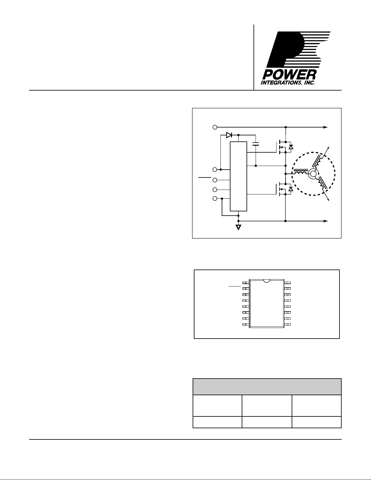
Description
The INT100 half-bridge driver IC provides gate drive for
external low-side and high-side MOSFET switches. The INT100
provides a simple, cost-effective interface between low-voltage
control logic and high-voltage loads. The INT100 is designed
to be used with rectified 110 V or 220 V supplies. Both highside and low-side switches can be controlled independently
from ground-referenced 5 V logic inputs.
V
DDH
HS OUT
V
DD
HS IN
LS IN
COM
Figure 1. Typical Application
HS RTN
LS OUT
LS
RTN
INT100
PI-1807-031296
Built-in protection logic prevents both switches from turning
on at the same time and shorting the high voltage supply. Pulsed
internal level shifting saves power and provides enhanced noise
immunity. The circuit is powered from a nominal 15 V supply
to provide adequate gate drive for external N-channel MOSFETs.
A floating high-side supply is derived from the low-voltage rail
by using a simple bootstrap technique.
Applications for the INT100 include motor drives, electronic
ballasts, and uninterruptible power supplies. Multiple devices
can also be used to implement full-bridge and multi-phase
configurations.
The INT100 is available in a 16-pin plastic SOIC package.
Figure 2. Pin Configuration.
ORDERING INFORMATION
PART
NUMBER
INT100S
PACKAGE
OUTLINE
ISOLATION
VOLTAGE
800 VS16A
June 1996
Page 2
INT100
V
DDH
LINEAR
REGULATOR
UV
LOCKOUT
V
DD
HS IN
LS IN
LINEAR
REGULATOR
UV
LOCKOUT
DISCRIMINATOR
PULSE
CIRCUIT
DELAY
DELAY
QS
R
HS OUT
HS RTN
LS OUT
COM
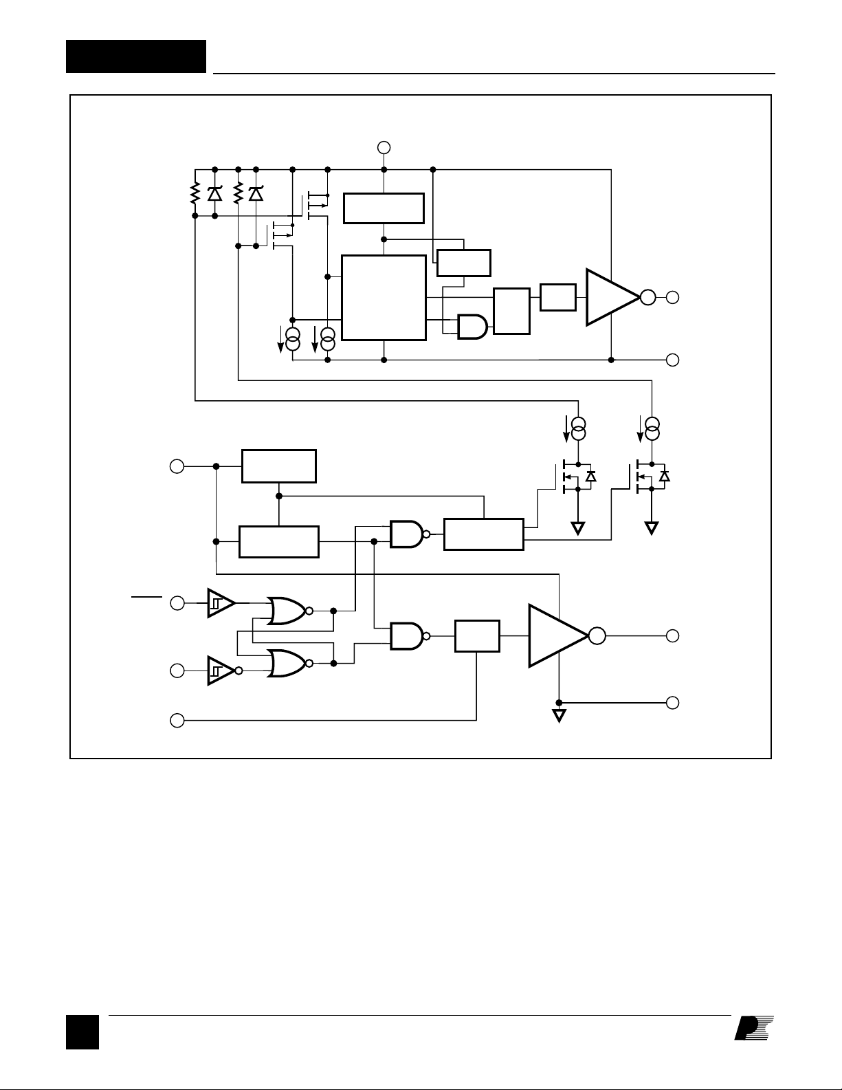
Figure 3. Functional Block Diagram of the INT100
C
2
6/96
LS RTN
PI-1083A-013194
Page 3
Pin Functional Description
INT100
Pin 1:
V
supplies power to the logic, high-
DD
side interface, and low-side driver.
Pin 7:
LS RTN is the power reference point for
the low-side circuitry, and should be
connected to the source of the low-side
Pin 2:
Active-low logic level input
HSINHSIN
HSIN
HSINHSIN
controls the high-side driver output.
MOSFET and to the COM pin.
Pin 8:
LS OUT is the driver output which
Pin 3:
controls the low-side MOSFET.
Active-high logic level input LS IN
controls the low-side driver output.
Pin 11:
HS OUT is the driver output which
Pin 4, 5:
controls the high-side MOSFET.
COM connection is used as the analog
reference point for the circuit.
INT100 Functional Description
5 V Regulators
Both low-side and high-side driver
circuits incorporate a 5 V linear regulator
circuit. The low-side regulator provides
the supply voltage for the control logic
and high-voltage level shift circuit. This
allows
HSIN
and LS IN to be directly
compatible with 5 V CMOS logic
without the need of an external 5 V
supply. The high-side regulator provides
the supply voltage for the noise rejection
circuitry and high-side control logic.
Undervoltage Lockout
The undervoltage lockout circuit for the
low-side driver disables both the LS
OUT and HS OUT pins whenever the
VDD power supply falls below typically
9.0 V, and maintains this condition until
the VDD power supply rises above
typically 9.35 V. This guarantees that
both MOSFETs will remain off during
power-up or fault conditions.
The undervoltage lockout circuit for the
high-side driver disables the HS OUT
pin whenever the V
power supply
DDH
falls below typically 9.0 V, and maintains
this condition until the V
DDH
power
supply rises above typically 9.35 V.
This guarantees that the high-side
MOSFET will be off during power-up
or fault conditions.
Level Shift
The level shift control circuitry of the
low-side driver is connected to integrated
high-voltage N-channel MOSFET
transistors which perform the levelshifting function for communication to
the high-side driver. Controlled current
capability allows the drain voltage to
float with the high-side driver. Two
individual channels produce a true
differential communication channel for
accurately controlling the high-side
driver in the presence of fast moving
high-voltage waveforms. The high
voltage level shift transistors employed
exhibit very low output capacitance,
minimizing the displacement currents
between the low-side and high-side
drivers during fast moving voltage
transients created during switching of
the external MOSFETs. As a result,
power dissipation is minimized and noise
immunity optimized.
The pulse circuit provides the two highvoltage level shifters with precise timing
Pin 12,13,14:
HS RTN is the power reference point
for the high-side circuitry, and should be
connected to the source of the high-side
MOSFET.
Pin 15:
V
supplies power to the high-side
DDH
control logic and output driver. This is
normally connected to a high-side
referenced bootstrap circuit or can be
supplied from a separate floating power
supply.
signals. These signals are used by the
discriminator to reject spurious noise.
The combination of differential
communication with the precise timing
provides maximum immunity to noise.
Simultaneous Conduction Lockout
A latch prevents the low-side driver and
high-side driver from being on at the
same time, regardless of the input signals.
Delay Circuit
The delay circuit matches the low-side
propagation delay with the combination
of the pulse circuit, high voltage level
shift, and high-side driver propagation
delays. This ensures that the low-side
driver and high-side driver will never be
on at the same time during switching
transitions in either direction.
Driver
The CMOS drive circuitry on both lowside and high-side driver ICs provide
drive power to the gates of the external
MOSFETs. The drivers consist of a
CMOS buffer capable of driving external
transistor gates at up to 15 V.
6/96
C
3
Page 4
INT100
100
0
0 100 200
Gate Charge (nC)
Switching Frequncy (kHz)
200
300
400
PI-1663-112095
VIN = 200 V
VIN = 300 V
VIN = 400 V
HV+
D1
V
DD
HS IN
LS IN
C1
1
2
3
4
5
6
7
8
16
15
14
13
12
11
10
9
INT100
HV-
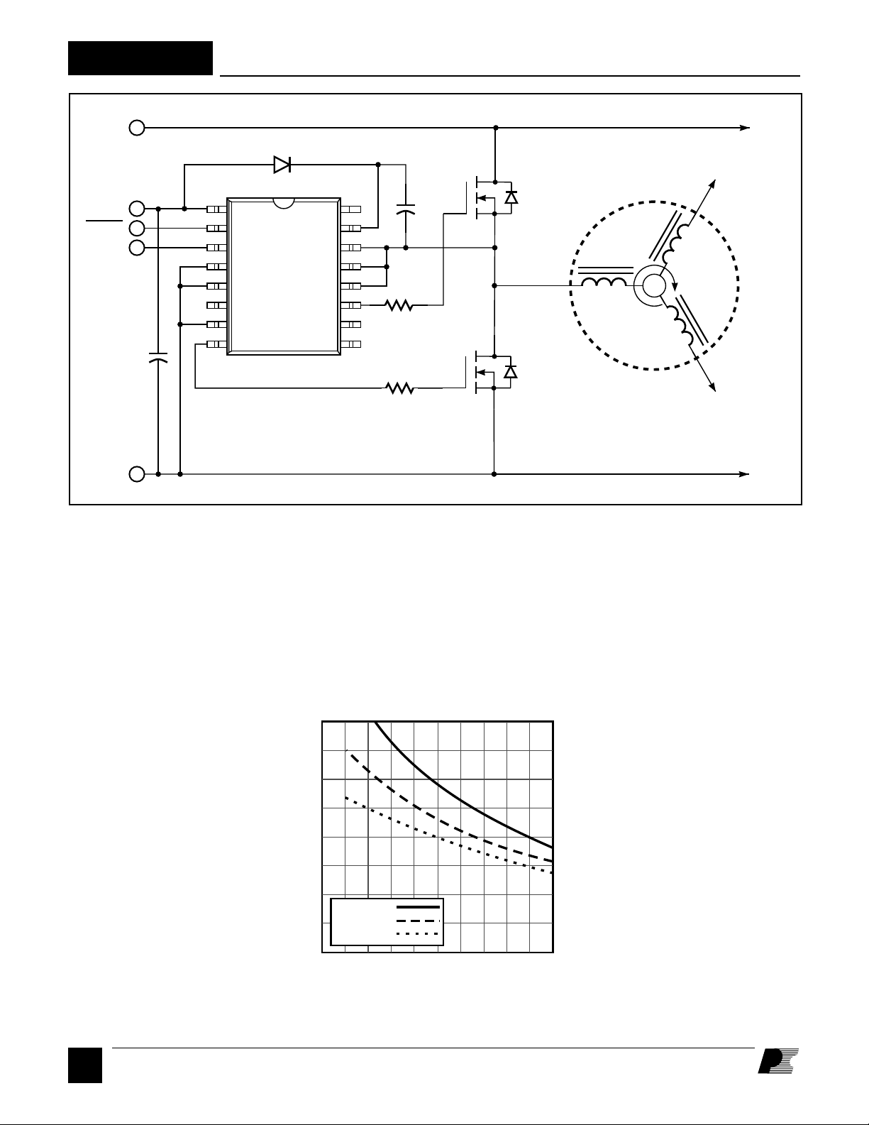
Figure 4. Using the INT100 in a 3-phase Configuration.
C2
Q2
PHASE 2
PHASE 1
R2
R1
Q1
PHASE 3
PI-1458-042695
C
4
6/96
Figure 5. Gate Charge versus Switching Frequency.
Page 5

General Circuit Operation
INT100
One phase of a three-phase motor drive
circuit is shown in Figure 4 to illustrate
an application of the INT100. The LS
IN signal directly controls MOSFET
Q1. The
HS IN
signal controls MOSFET
Q2 via the high voltage level shift
transistors communicating with the highside driver. The INT100 will ignore
input signals that would command both
Q1 and Q2 to conduct simultaneously,
protecting against shorting the HV+ bus
to HV-.
Local bypassing for the low-side driver
is provided by C1. Bootstrap bias for the
high-side driver is provided by D1 and
C2. Slew rate and effects of parasitic
oscillations in the load waveforms are
controlled by resistors R1 and R2.
The inputs are designed to be compatible
with 5 V CMOS logic levels and should
not be connected to VDD. Normal CMOS
power supply sequencing should be
observed. The order of signal application
should be VDD, logic signals, and then
HV+. VDD should be supplied from a
low impedance voltage source.
The output returns (HS RTN and LS
RTN) are isolated from one another by
the internal high-voltage MOSFET level
shifters. The level shift circuitry is
designed to operate properly even when
the HS RTN swings as much as 5 V
below the LS RTN pin with V
DDH
biased
at 15 V. The INT100 will also safely
tolerate more negative voltages (as low
as -V
below LS RTN).
DDH
Maximum frequency of operation is
limited by power dissipation due to highvoltage switching, gate charge, and bias
power. Figure 5 indicates the maximum
switching frequency as a function of
input voltage and gate charge. For higher
ambient temperatures, the switching
frequency should be derated linearly.
The bootstrap capacitor must be large
enough to provide bias current over the
entire on-time of the high-side driver
without significant voltage sag or decay.
The high-side MOSFET gate charge
must also be supplied at the desired
switching frequency. Figure 6 shows
the maximum high-side on-time versus
gate charge of the external MOSFET.
Applications with extremely long highside on times require special techniques
discussed in AN-10.
The high-side driver is latched on and
off by the edges of the appropriate lowside logic signal. The high-side driver
will latch off and stay off if the bootstrap
capacitor discharges below the
undervoltage lockout threshold.
Undervoltage lockout-induced turn off
can occur during conditions such as
power ramp up, motor start, or low speed
operation.
C
BOOTSTRAP
1000
100
10
1
0.1
QG = 100 nC
QG = 20 nC
vs. ON TIME
Bootstrap Capacitance (µF)
0.01
0.01 0.1 1 10 100
High Side On Time (ms)
Figure 6. High-side On Time versus Bootstrap Capacitor.
PI-566B-030692
6/96
C
5
Page 6

INT100
ABSOLUTE MAXIMUM RATINGS
VDD Voltage ................................................................16.5 V
V
Voltage ........................................... HS RTN + 16.5 V
DDH
HS RTN............................................. 800 V - V
DDH
to -V
DDH
HS RTN Slew Rate ...................................................10V/ns
Logic Input Voltage ...................................... -0.3V to 5.5 V
LS OUT Voltage ................ LS RTN - 0.3 V to VDD + 0.3 V
HS OUT Voltage..............HS RTN - 0.3 V to V
DDH
+ 0.3 V
Storage Temperature ....................................... –65 to 125°C
Conditions
(Unless Otherwise Specified)
Parameter Symbol V
= VDD = 15 V Min Typ Max Units
DDH
HS RTN = LS RTN = COM = 0 V
TA = -40 to 85°C
LOGIC
Input Current,
High or Low
Input Voltage
High
I
IH, IIL
V
IH
VIH = 4.0 V
VIL = 1.0 V
1
Ambient Temperature........................................ -40 to 85°C
Junction Temperature ................................................. 150°C
Lead Temperature
(2)
. ................................................... 260°C
Power Dissipation (TA = 25°C).................................. 2.3 W
(TA = 70°C).................................. 1.5 W
Thermal Impedance (θJA)......................................... 55°C/W
1. Unless noted, all voltages referenced to COM, TA = 25°C
2. 1/16" from case for 5 seconds.
0 10 150
-20 0 20
4.0
µA
V
Input Voltage
Low
Input Voltage
Hysteresis
LS OUT/HS OUT
Output
Voltage High
Output
Voltage Low
Output Short
Circuit Current
Turn-on Delay
Time
Rise
Time
Turn-off Delay
Time
V
V
V
OH
V
OL
I
OS
t
d(on)LS
t
d(on)HS
t
t
d(off)LS
t
d(off)HS
HY
r
IL
1.0
0.3 0.7
LS OUT
VDD-1.0 VDD-0.5
Io= -20 mA
HS OUT
Io= 40 mA
Vo= 0 V
V
DDH
-150
-1.0 V
-0.5
DDH
0.3 1.0
See Note 1
Vo= 15 V
LS OUT
300
0.6 1.0
See Figure 7
HS OUT
See Figure 7
LS OUT
1.0 1.5
80 120
500 1000
See Figure 7
HS OUT
420 600
V
V
V
V
mA
µs
ns
ns
Fall
Time
6
C
6/96
t
f
See Figure 7
50 100
ns
Page 7

Parameter Symbol V
LEVEL SHIFT
Breakdown
Voltage
BV
DSS
Conditions
(Unless Otherwise Specified)
= VDD = 15 V Min Typ Max Units
DDH
HS RTN = LS RTN = COM = 0 V
TA = -40 to 85°C
V
= HS OUT = HS RTN
DDH
I
= 100 µA
HS RTN
800
INT100
V
Leakage
Current
I
HS RTN)
Interface
Capacitance
SYSTEM RESPONSE
Deadtime (Low
Off to High On)
Deadtime (High
Off to Low On)
Dt
Dt
P+
P-
UNDERVOLTAGE LOCKOUT
V
Input UV
Trip-off Voltage
DD(UV)
V
DDH(UV)
Input UV
Hysteresis
SUPPLY
Supply
Current
IDD, I
DDH
V
= HS OUT = HS RTN = 500 V
DDH
V
= HS OUT = HS RTN = 500 V
DDH
See Figure 7
See Figure 7
See Note 2
0.2 30
20
0 450
0 300
8.5 9.0 10
175 350
1.5 3.0
µA
pF
ns
ns
V
mV
mA
Supply
Voltage
NOTES:
1. Applying a short circuit to the LS OUT or HS OUT pin for more than 500 µs will exceed the thermal rating of the
package, resulting in destruction of the part.
2. VDD, V
supply must have less than 30Ω output impedance.
DDH
VDD, V
DDH
10 16
6/96
V
C
7
Page 8

INT100
INPUT
CL
1000 pF
5 V
0 V
15 V
0 V
15 V
0 V
t
d(off)LS
Dt
50%
t
f
90%
50%
10% 10%
p+
50%
INPUT
15 V
1
2
3
4
5
6
7
8
16
15
14
13
12
INT100
11
10
9
100 nF
CL
1000 pF
LS OUT
1 µF
HS OUT
50% 50%
t
d(on)LS
t
r
90%
50%
Dt
p-
t
d(off)HS
t
f
90%
50%
10% 10%
t
d(on)HS
t
r
90%
PI-1459-042695
Figure 7. Switching Time/Deadtime Test Circuit.
BREAKDOWN vs. TEMPERATURE
1.1
1.0
PI-176B-051391
PACKAGE POWER DERATING
2.5
2.0
1.5
1
PI-1808-032096
(Normalized to 25°C)
Breakdown Voltage (V)
0.9
-50 -25 0 25 50 75 100 125 150
Junction Temperature (°C)
C
8
6/96
0.5
Power Dissipation (W)
0
0 25 50 75 100 125
Junction Temperature (°C)
150
Page 9

INT100
S16A Plastic SO-16 (W)
DIM inches mm
A .398-.413 10.10-10.50
B .050 BSC 1.27 BSC
C .014-.018 0.36-0.46
E .093-.104 2.35-2.65
F .004-.012 0.10-0.30
J .394-.418 10.01-10.62
L .009-.012 0.23-0.32
M .020-.040 0.51-1.02
N .291-.299 7.40-7.60
Notes:
1. Package dimensions conform to JEDEC
specification MS-013-AA for standard small outline
(SO) package, 16 leads, 7.50 mm (.300 inch) body
width (issue A, June 1985).
2. Controlling dimensions are in mm.
3. Dimensions are for the molded body and do not
include mold flash or protrusions. Mold flash or
protrusions shall not exceed .15 mm (.006 inch) on
any side.
4. Pin 1 side identified by chamfer on top edge of
the package body or indent on Pin 1 end.
16
1
(3)
A
9
(3)
N
8
J
L
E
C
B
F
0-8˚ TYP.
M
PI-1846-050196
6/96
C
9
Page 10

INT100
Notes
10
C
6/96
Page 11

Notes
INT100
6/96
C
11
Page 12

INT100
Power Integrations reserves the right to make changes to its products at any time to improve reliability or manufacturability.
Power Integrations does not assume any liability arising from the use of any device or circuit described herein, nor does it
convey any license under its patent rights or the rights of others.
PI Logo and
TOPSwitch
are registered trademarks of Power Integrations, Inc.
©Copyright 1994, Power Integrations, Inc. 477 N. Mathilda Avenue, Sunnyvale, CA 94086
WORLD HEADQUARTERS
Power Integrations, Inc.
477 N. Mathilda Avenue
Sunnyvale, CA 94086
USA
Main: 408•523•9200
Customer Service:
Phone: 408•523•9265
Fax: 408•523•9365
JAPAN
Power Integrations, K.K.
Keihin-Tatemono 1st Bldg.
12-20 Shin-Yokohoma 2-Chome, Kohoku-ku
Yokohama-shi, Kanagawa 222 Japan
Phone: 81•(0)•45•471•1021
Fax: 81•(0)•45•471•3717
AMERICAS
For Your Nearest Sales/Rep Office
Please Contact Customer Service
Phone: 408•523•9265
Fax: 408•523•9365
ASIA & OCEANIA
For Your Nearest Sales/Rep Office
Please Contact Customer Service
Phone: 408•523•9265
Fax: 408•523•9365
EUROPE & AFRICA
Power Integrations (Europe) Ltd.
Mountbatten House
Fairacres
Windsor SL4 4LE
United Kingdom
Phone: 44•(0)•1753•622•208
Fax: 44•(0)•1753•622•209
APPLICATIONS HOTLINE
World Wide 408•523•9260
APPLICATIONS FAX
Americas 408•523•9361
Europe/Africa
44•(0)•1753•622•209
Japan 81•(0)•45•471•3717
Asia/Oceania 408•523•9364
12
C
6/96
 Loading...