

Page 1
INFRARED REMOTE CONTROL
TRANSMITTER RC-5
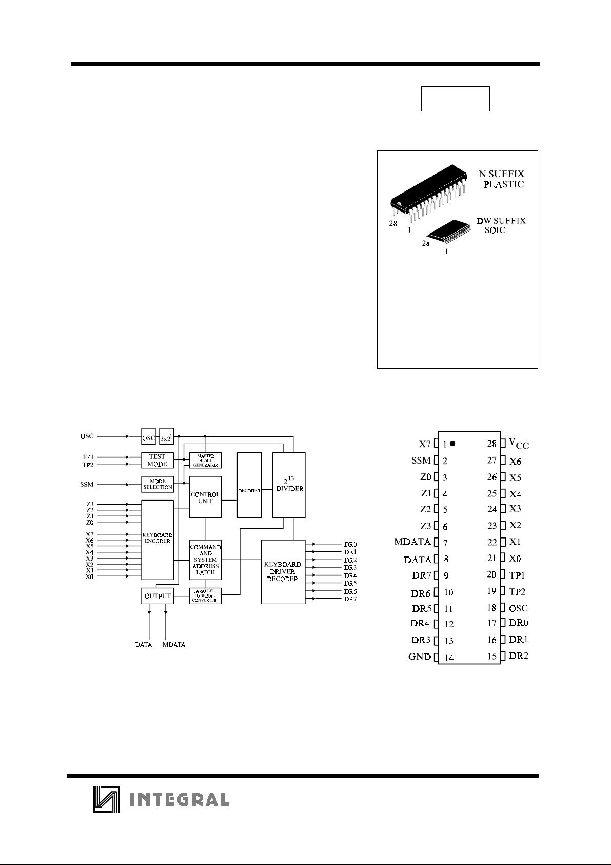
The INA3010 is intended as a general purpose (RC-5) infrared
remote control system for use where a low voltage supply and a large
debounce time are expected. The device can generate 2048 different
commands and utilizes a keyboard with a single pole switch for each
key. The command are arranged so that 32 systems can be addressed,
each system containing 64 different commands. The keyboard
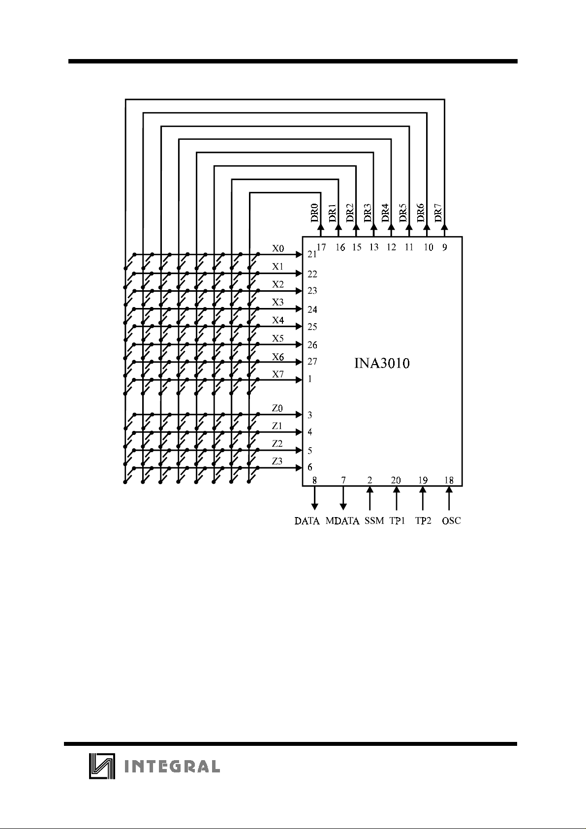
interconnection is illustrated by Fig.1.
INA3010
INA3010
• Low voltage requirement
• Single pin oscillator
• Biphase transmission technique
• Test mode facility
BLOCK DIAGRAM
ORDERING INFORMATION
INA3010N Plastic
INA3010DW SOIC
TA = -25° to 85° C
for all packages
.
PIN ASSIGNMENT
1
Page 2
INA3010
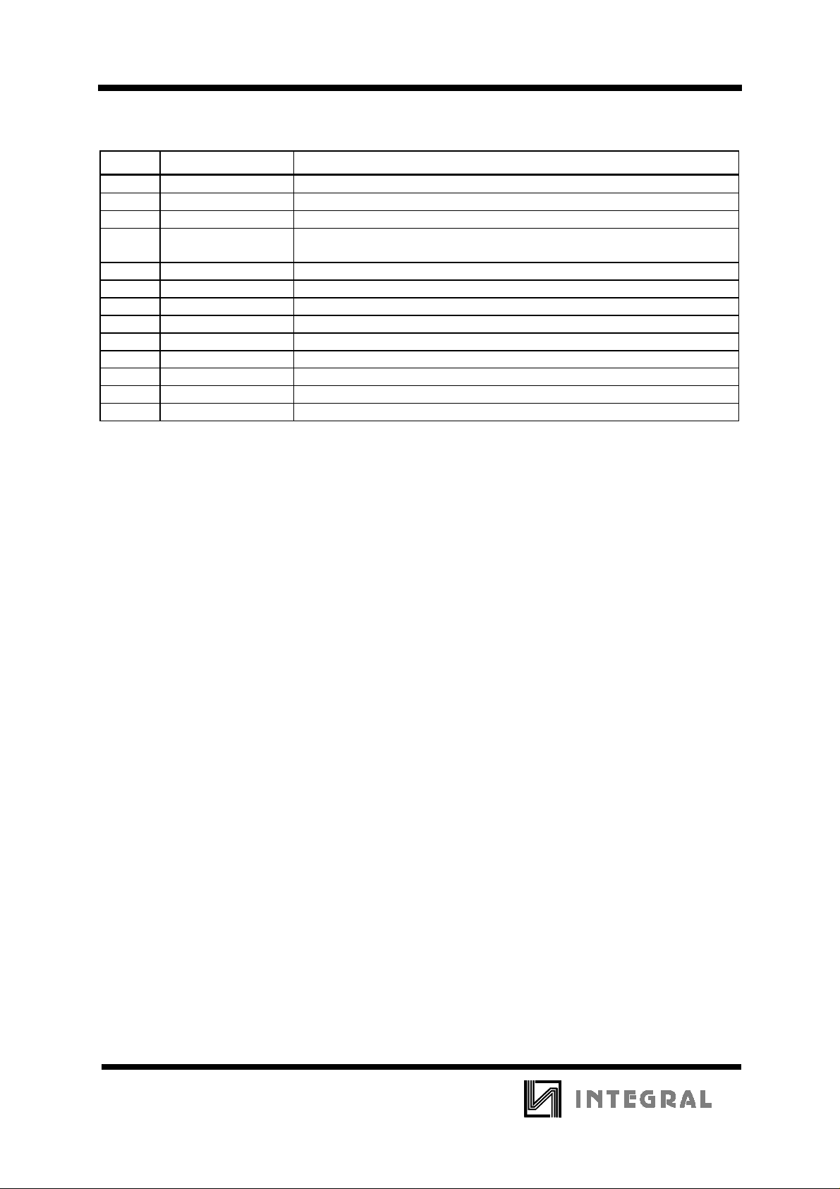
PIN DESCRIPTION
PIN No DESIGNATION DESCRIPTION
1 X7 (IPU) sense input from key matrix
2 SSM (I) system mode selection input
3-6 Z0-Z3 (IPU) sense inputs from key matrix
7 MDATA (OP3) generated output data modulated with 1/2 the oscillator frequency at a 25%
duty factor
8 DATA (OP3) generated output information
9-13 DR7-DR3 (ODN) scan drivers
14 GND ground (0V)
15-17 DR2-DR0 (ODN) scan drivers
18 OSC (I) oscillator input
19 TP2 (I) test point 2
20 TP1 (I) test point 1
21-27 X0-X6 (IPU) sense inputs from key matrix
28 Vcc (I) voltage supply
(I) = input
(IPU) = input with p-channel pull-up transistor
(ODN) = output with open drain n-channel transistor
(OP3) = output 3-state
FUNCTIONAL DESCRIPTION
Keyboard operation
Every connection of one X-input and one DR-output will be recognized as a legal key operation and will cause
the device to generate the corresponding code. The same applies to every connection of one Z-input to one DRoutput with the proviso that SSM must be LOW. When SSM is HIGH a wired connection must exist between a
Z-input and DR-output. If no connection is present the system number will not be generated. Activating two or
more X-inputs, Z-inputs or Z-inputs and X-inputs at the same time is an illegal action and inhibits further activity
(oscillator will not start).
When one X- or Z-input is connected to more than one DR-output, the last scan signal will be considered as
legal.
The maximum value of the contact series resistance of the switched keyboard is 7KΩ.
Inputs
In the quiescent state the command inputs X0 to X7 are held HIGH by an internal pull-up transistor. When the
system mode selection (SSM) input is LOW and the system is quiescent, the system inputs Z0 to Z3 are also held
HIGH by an internal pull-up transistor. When SSM is HIGH the pull-up transistor for the Z-inputs is switched
off, in order to prevent current flow, and a wired connection in the Z-DR matrix provides the system number.
Outputs
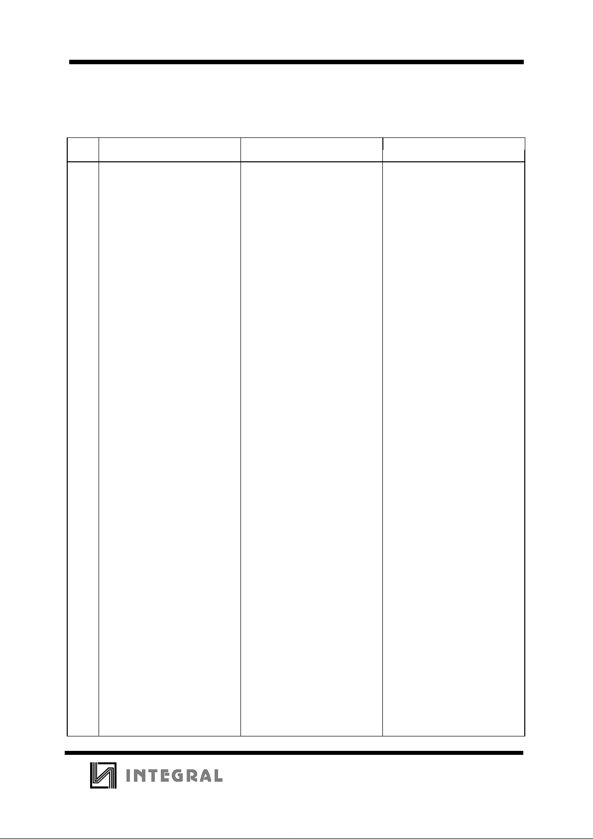
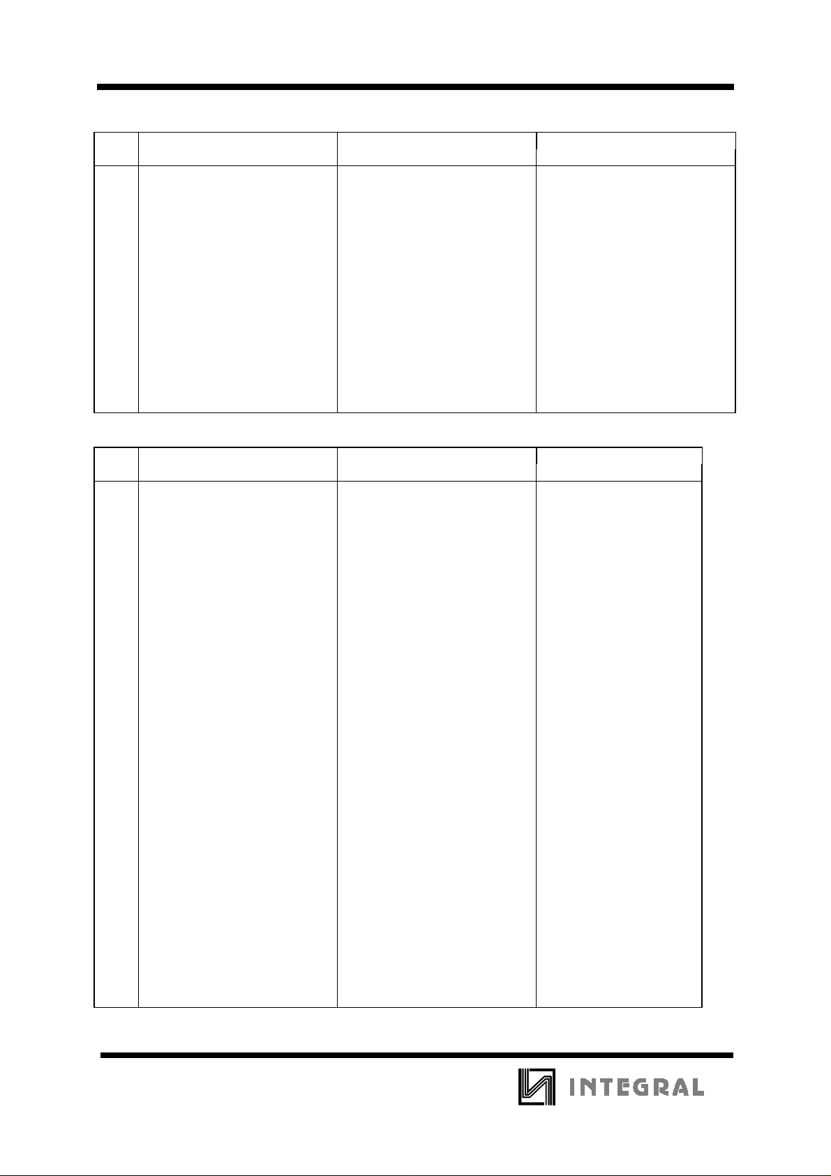
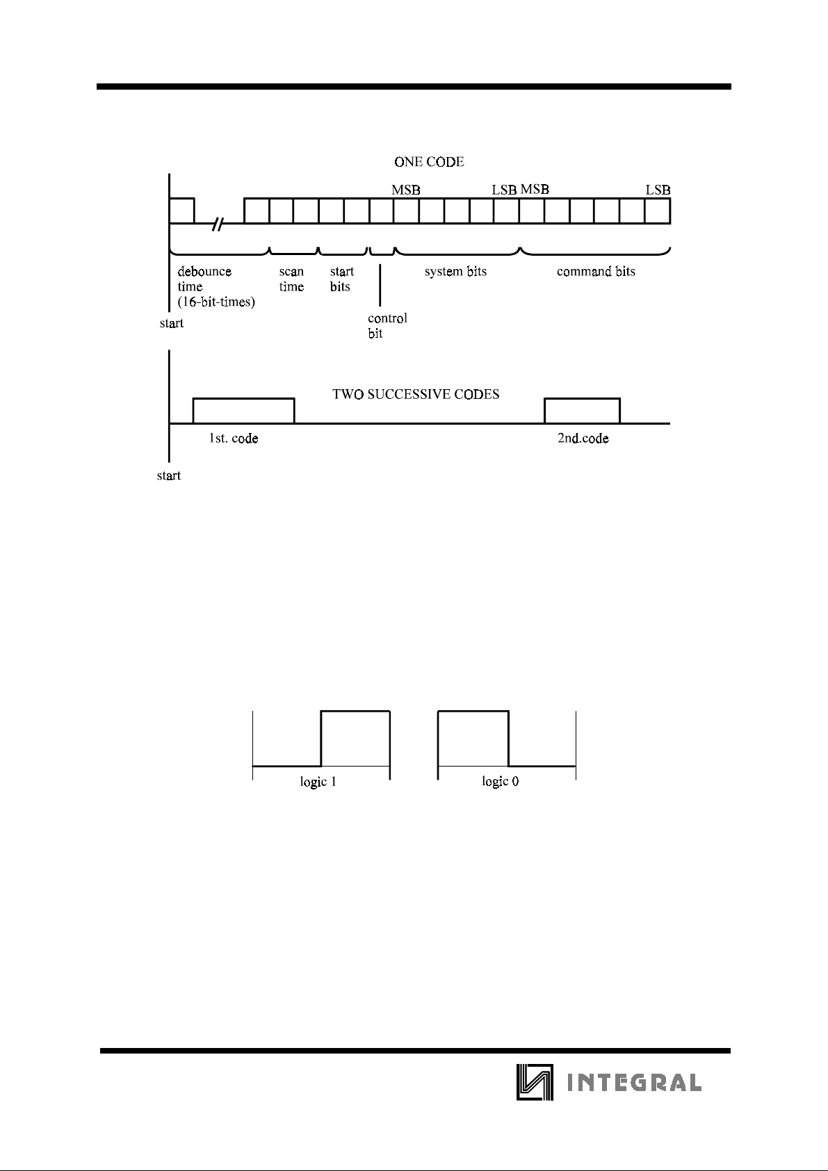
The output signal DATA transmits the generated information in accordance with the format illustrated by Fig.2
and Tables 1 and 2. The code is transmitted using a biphase technique as illustrated by Fig.3. The code consists
of four parts:
• Start part - 1.5 bits (2 x logic 1)
• Control part - 1 bit
• System part - 5 bits
• Command part - 6 bits
The output signal MDATA transmits the generated information modulated by 1/12 of the oscillator frequency
with a 50% duty factor.
In the quiescent state both DATA and MDATA are non-conducting (3-state outputs).
The scan driver outputs DR0 to DR7 are open drain n-channel transistors and conduct when the circuit is
quiescent. After a legal key operation the scanning cycle is started and the outputs switched to the conductive
state one by one. The DR-outputs were switched off at the end of the preceding debounce cycle.
2
Page 3
INA3010
Table 1
Code X-lines DR-lines Command bits
no. 0123456701234567 5 4 3 2 1 0
10 x x 001010
11 x x 001011
12 x x 001100
13 x x 001101
14 x x 001110
15 x x001111
16 x x 010000
17 x x 010001
18 x x 010010
19 x x 010011
20 x x 010100
21 x x 010101
22 x x 010110
23 x x010111
24 x x 011000
25 x x 011001
26 x x 011010
27 x x 011011
28 x x 011100
29 x x 011101
30 x x 011110
31 x x011111
32 x x 100000
33 x x 100001
34 x x 100010
35 x x 100011
36 x x 100100
37 x x 100101
38 x x 100110
39 x x100111
40 x x 101000
41 x x 101001
42 x x 101010
43 x x 101011
44 x x 101100
45 x x 101101
46 x x 101110
47 x x101111
48 x x 110000
Table 1
Command matrix (X-DR)
0x x 000000
1x x 000001
2x x 000010
3x x 000011
4x x 000100
5x x 000101
6x x 000110
7x x000111
8 x x 001000
9 x x 001001
Command matrix (X-DR) (Continued)
3
Page 4
INA3010
Code X-lines DR-lines Command bits
no. 0123456701234567 5 4 3 2 1 0
49 x x 110001
50 x x 110010
51 x x 110011
52 x x 110100
53 x x 110101
54 x x 110110
55 x x110111
56 xx 111000
57 x x 111001
58 x x 111010
59 x x 111011
60 x x 111100
61 x x 111101
62 x x 111110
63 x x111111
Table 2
Code X-lines DR-lines System bits
no. 0123456701234567 4 3 2 1 0
10 x x 01010
11 x x 01011
12 x x 01100
13 x x 01101
14 x x 01110
15 x x01111
16 x x 10000
17 x x 10001
18 x x 10010
19 x x 10011
20 x x 10100
21 x x 10101
22 x x 10110
23 x x10111
24 x x 11000
25 x x 11001
26 x x 11010
27 x x 11011
28 x x 11100
29 x x 11101
30 x x 11110
31 x x11111
System matrix (Z-DR)
0x x 00000
1x x 00001
2x x 00010
3x x 00011
4x x 00100
5x x 00101
6x x 00110
7x x00111
8 x x 01000
9 x x 01001
4
Page 5
INA3010
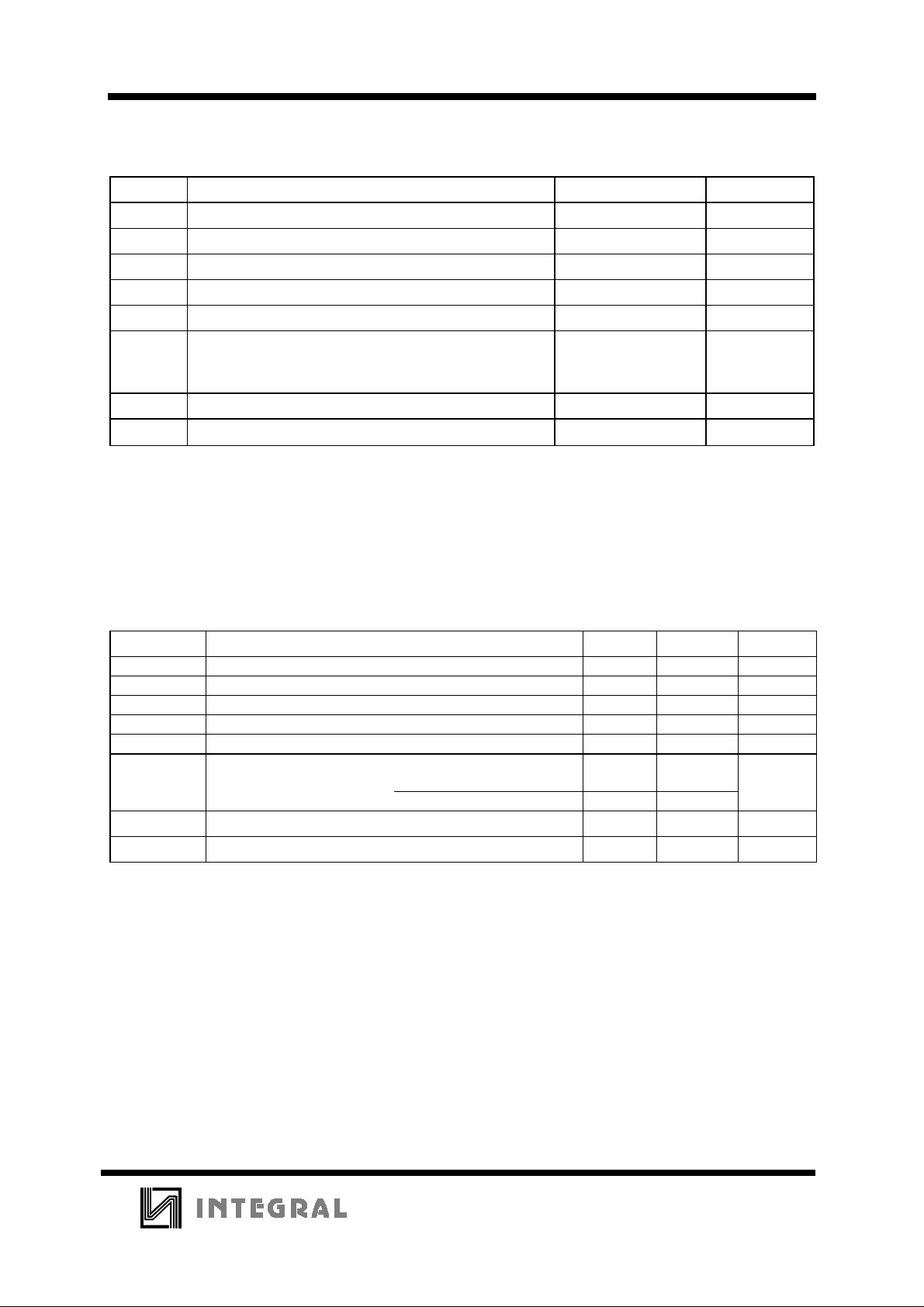
MAXIMUM RATINGS
*
Symbol Parameter Value Unit
V
CC
V
V
OUT
I
IN
I
OUT
DC Supply Voltage (Referenced to GND) -0.5 to +8.5 V
DC Input Voltage (Referenced to GND)* -0.5 to VCC +0.5 V
IN
DC Output Voltage (Referenced to GND)* -0.5 to VCC +0.5 V
DC Input Current
DC Output Current
±10
±10
Maximum Power Dissipation
P
DO
P
DO
P
OSC output
other outputs
Power Dissipation in Still Air 200 mW
D
50
100
Tstg Storage Temperature -65 to +150
*VCC + 0.5 must not exceeed 9.0V..
*
Maximum Ratings are those values beyond which damage to the device may occur.
Functional operation should be restricted to the Recommended Operating Conditions.
+Derating - Plastic DIP: - 10 mW/°C from 65° to 85°C
SOIC Package: : - 7 mW/°C from 65° to 85°C
mA
mA
mW
mW
°C
RECOMMENDED OPERATING CONDITIONS
Symbol Parameter Min Max Unit
V
CC
V
IH
V
IL
V
OUT
I
IN
I
OL
I
OH
T
A
This device c ontains p rote ction ci rcuitr y to guard a gainst damage d ue to high st atic voltages or electr ic
fields. However, precautions must be taken to avoid applications of any voltage higher than maximum rated
voltages to this high-impedance circuit. For proper operation, V
GND≤(V
Unused inputs must always be tied to an appropriate logic voltage level (e.g., either GND or V
Unused outputs must be left open.
DC Supply voltage (Reference to GND) 2.0 7.0 V
DC Input voltage (HIGH) 0.7V
CC
DC Input voltage (LOW) 0 0.3V
DC Output Voltage (MDATA, DATA) - 7.0 V
DC Input Current - ±10 mA
DC Output Current (LOW) -
pins 7,8 0.6 mA
pins 9-13; 15-17 0.3
DC Output Current (MDATA, DATA)
Operating Temperature, All Package Types
IN
or V
OUT
)≤VCC.
and V
IN
OUT
--0.4mA
-25 85
should be constrained to the range
V
CC
CC
V
V
o
C
CC
).
5
Page 6
INA3010
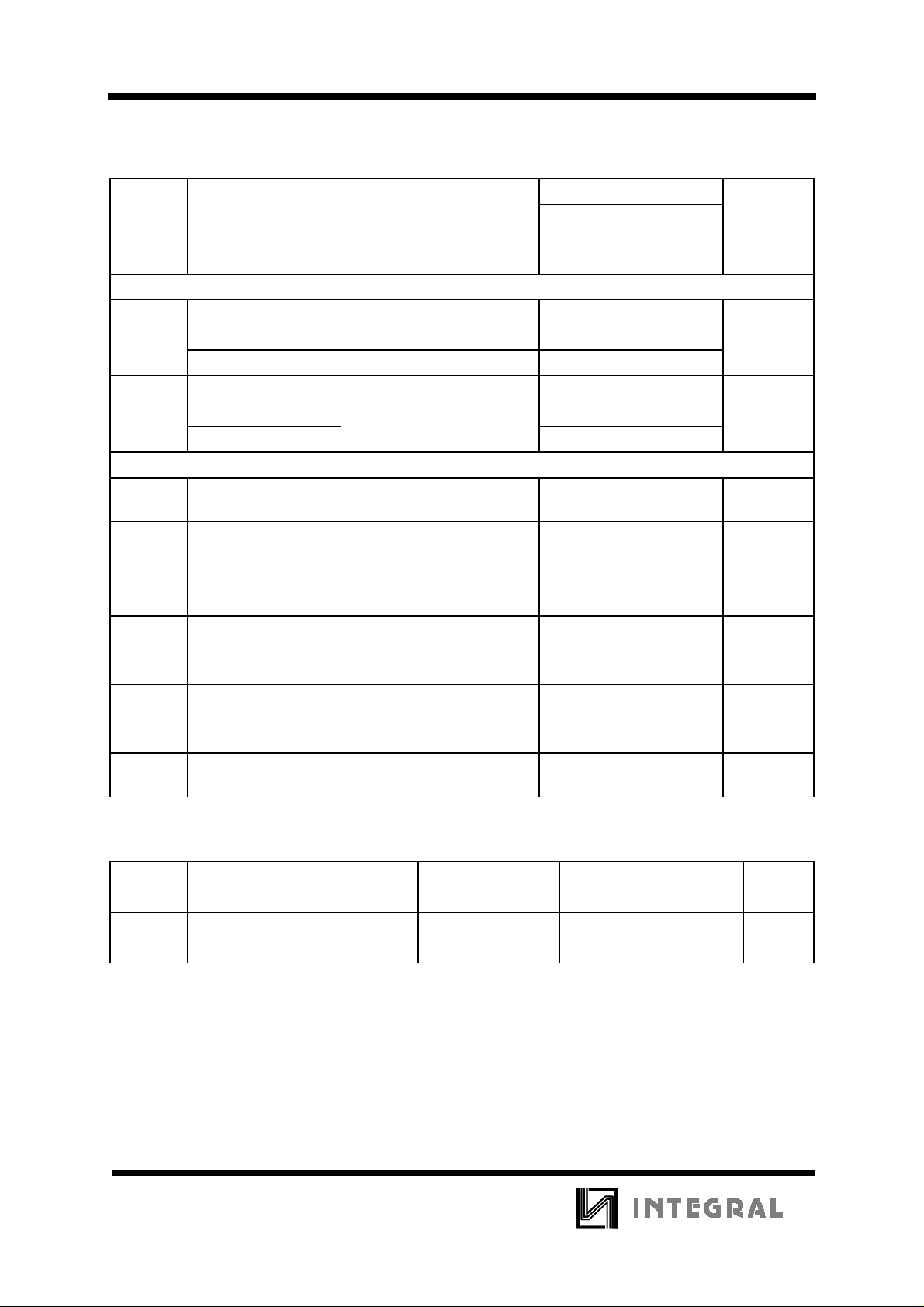
DC ELECTRICAL CHARACTERISTICS
= 2.0 to 7.0V unless otherwise specified, TA=-25 to +70°C)
(V
CC
(Voltage Reference to GND)
Guaranteed Limits
Symbol Parameter Test Conditions Min Max Unit
I
CC
Quiscent supply
current
UIL=0B; VIH=V
I
=0 mA at all outputs
OUT
CC
40
INPUTS
I
IN
I
LI
Input current
VIL=0V
Pins 01, 03-06; 21-27
Pin 18 VIL=0V; VIH=V
Input leakage current
VIL=0V; VIH=V
Pins 01-06;19-27
CC
CC
-10 -600
3.0 33
-
±10
Pin 18 - -20
OUTPUTS
V
OH
V
OL
I
LO
Output voltage
HIGH, pins 07-08
Output voltage LOW
Pins 07-08
IOH=-0.4mA
V
=0.3 V
IL
CC
IOL=0.6mA
=0V, VHI=0.7V
V
IL
Pins 9-13; 15-17 IOL=0.3mA, VIL=0V,
V
=0.7V
Output leakage
current
IH
VO=VCC, VIH=VCC,
V
OH=VCC
CC
VCC-0.3 - V
-0.3V
CC
-0.3V
-10
Pins 07-13; 15-17 -
I
LO
Output leakage
VO=0V, VIH=VCC, VOL=0V - -20
current
Pins 07-08 -
I
OH
DC Output Current
VIL=0V; VIH=VCC; VOH=V
CC
10
Pins 9-13; 15-17
µA
µA
µA
µA
µA
µA
AC ELECTRICAL CHARACTERISTICS
TA=-25 to +85°C; VCC=2.0 to 7.0 V unless otherwise specified
Symbol Parameter Test Condition Guaranteed Limits
Typ Max Unit
Oscillator frequency CL=160pF
f
OSC
6
operational 432 450 KHz
Page 7
INA3010
Figure 1. Keyboard interconnection
7
Page 8
INA3010
Where: debounce time+scan time=18 bit-temes
repetition time=4x16 bit times
Figure 2. Data output format
Where: 1 bit-time=3.28 x T
Figure 3. Biphase transmission technique
=1.778 ms (typ.)
OSC
8
 Loading...