

Page 1
Dual, Low Power, Single-Supply
DIFFERENCE AMPLIFIER
©1998 Burr-Brown Corporation PDS-1488A Printed in U.S.A. December, 1998
®
FEATURES
● DESIGNED FOR LOW COST
● LOW QUIESCENT CURRENT:
160µA per Amplifier
● WIDE POWER SUPPLY RANGE:
Single Supply: 2.7V to 36V
Dual Supplies: ±1.35V to ±18V
● LOW GAIN ERROR: ±0.05% max
● LOW NONLINEARITY: 0.001% max
● HIGH CMRR: 90dB
● HIGHLY VERSATILE CIRCUIT
● EASY TO USE
● SO-14 PACKAGE
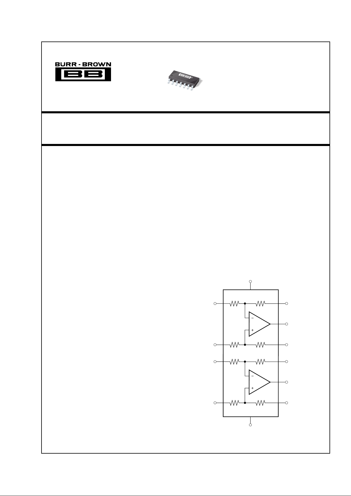
INA2132
DESCRIPTION
The INA2132 is a dual low power, unity-gain difference amplifier offering excellent value at very low
cost. Each channel consists of a precision op amp with
a laser-trimmed precision resistor network, providing
accurate gain and high common-mode rejection. Excellent TCR tracking of the resistors maintains gain
accuracy and common-mode rejection over temperature. The internal op amp’s common-mode range
extends to the negative supply—ideal for single-supply applications.
The difference amplifier is the foundation of many
commonly used circuits. The INA2132 provides this
circuit function without using an expensive precision
resistor network. The INA2132 is available in the
SO-14 surface-mount package and is specified for
operation over the extended industrial temperature
range, –40°C to +85°C.
A single version of this product with similar specifications is also available. See the INA132 data sheet
for details.
APPLICATIONS
● DIFFERENTIAL INPUT AMPLIFIER
● INSTRUMENTATION AMPLIFIER
BUILDING BLOCK
● UNITY-GAIN INVERTING AMPLIFIER
● G = 1/2 AMPLIFIER
● G = 2 AMPLIFIER
● SUMMING AMPLIFIER
● DIFFERENTIAL CURRENT RECEIVER
● VOLTAGE-CONTROLLED CURRENT SOURCE
● BATTERY-POWERED SYSTEMS
● GROUND LOOP ELIMINATOR
International Airport Industrial Park • Mailing Address: PO Box 11400, Tucson, AZ 85734 • Street Address: 6730 S. Tucson Blvd., Tucson, AZ 85706 • Tel: (520) 746-1111
Twx: 910-952-1111 • Internet: http://www.burr-brown.com/ • Cable: BBRCORP • Telex: 066-6491 • FAX: (520) 889-1510 • Immediate Product Info: (800) 548-6132
Sense A
INA2132
Out A
V+
Ref A
–In A
+In A
12
13
14
2
11
V–
4
3
40kΩ 40kΩ
40kΩ 40kΩ
40kΩ 40kΩ
40kΩ 40kΩ
B
A
Sense B
Out B
Ref B
–In B
+In B
10
9
8
6
5
INA2132
Page 2
2
®
INA2132
PARAMETER CONDITIONS MIN TYP MAX MIN TYP MAX UNITS
OFFSET VOLTAGE
(1)
RTO
Initial V
OS
±75 ±250 ✻ ±500 µV
vs Temperature dV
OS
/dT ±1 ±5 ✻ ±10 µV/°C
vs Power Supply PSRR V
S
= ±1.35V to ±18V ±5 ±30 ✻✻µV/V
vs Time 0.3 ✻ µV/mo
Channel Separation
(2)
dc 0.04 µV/V
INPUT IMPEDANCE
(3)
Differential 80 ✻ kΩ
Common-Mode 40 ✻ kΩ
INPUT VOLTAGE RANGE
Common-Mode Voltage Range
(4)
VO = 0V 2 (V–) 2 (V+) –2 ✻✻V
Common-Mode Rejection Ratio
CMRR
VCM = –30V to 28V, RS = 0Ω 80 90 74 ✻ dB
OUTPUT VOLTAGE NOISE
(5)
RTO
f = 0.1Hz to 10Hz 1.6 ✻ µVp-p
f = 1kHz 65 ✻ nV/√Hz
GAIN
Initial 1 ✻ V/V
Error V
O
= –14V to 13.5V ±0.01 ±0.05 ✻ ±0.1 %
vs Temperature ±1 ±10 ✻✻ppm/°C
Nonlinearity V
O
= –14V to 13.5V ±0.0001 ±0.001 ✻ ±0.002 % of FS
OUTPUT
Voltage, Positive R
L
= 100kΩ to Ground (V+) –1 (V+) –0.8 ✻✻ V
Negative R
L
= 100kΩ to Ground (V–) +0.5 (V–) +0.15 ✻✻ V
Positive R
L
= 10kΩ to Ground (V+) –1.5 (V+) –0.8 ✻✻ V
Negative RL = 10kΩ to Ground (V–) +1 (V–) +0.25 ✻✻ V
Current Limit, per Amplifier Continuous to Common ±12 ✻ mA
Capacitive Load (stable operation) 10 ✻ nF
FREQUENCY RESPONSE
Small-Signal Bandwidth –3dB 300 ✻ kHz
Slew Rate SR 0.1 ✻ V/µs
Settling Time: 0.1% V
O
= 10V Step 85 ✻ µs
0.01% V
O
= 10V Step 88 ✻ µs
Overload Recovery Time 50% Overdrive 7 ✻ µs
POWER SUPPLY
Rated Voltage V
S
±15 ✻ V
Voltage Range ±1.35 ±18 ✻✻V
Quiescent Current (per amplifier) I
Q
IO = 0mA ±160 ±185 ✻✻ µA
TEMPERATURE RANGE
Specification –40 +85 ✻✻°C
Operation –55 +125 ✻✻°C
Storage –55 +125 ✻✻°C
Thermal Resistance
θ
JA
100 ✻ °C/W
✻ Specifications the same as INA2132U.
NOTES: (1) Includes effects of amplifier’s input bias and offset currents. (2) Measured output offset change of one channel for a full-scale swing (V
O
= –14V
to 13.5V) on the opposite channel. (3) 40kΩ resistors are ratio matched but have ±20% absolute value. (4) 2 (V–) –V
REF
< VCM < 2 ((V+) –1) –V
REF
. For more detail,
see Applications Information section. (5) Includes effects of amplifier’s input current noise and thermal noise contribution of resistor network.
SPECIFICATIONS: VS = ±15V
At TA = +25°C, RL = 10kΩ connected to ground, and reference pins connected to ground unless otherwise noted.
The information provided herein is believed to be reliable; however, BURR-BROWN assumes no responsibility for inaccuracies or omissions. BURR-BROWN assumes
no responsibility for the use of this information, and all use of such information shall be entirely at the user’s own risk. Prices and specifications are subject to change
without notice. No patent rights or licenses to any of the circuits described herein are implied or granted to any third party. BURR-BROWN does not authorize or warrant
any BURR-BROWN product for use in life support devices and/or systems.
INA2132U INA2132UA
Page 3
3
®
INA2132
SPECIFICATIONS: VS = +5V Single Supply
At TA = +25°C, RL = 10kΩ connected to VS/2, and reference pin connected to VS/2, unless otherwise noted.
INA2132U INA2132UA
PARAMETER CONDITIONS MIN TYP MAX MIN TYP MAX UNITS
OFFSET VOLTAGE
(1)
RTO
Initial V
OS
±150 ±500 ✻ ±750 µV
vs Temperature dV
OS
/dT ±2 ✻ µV/°C
INPUT VOLTAGE RANGE
Common-Mode Voltage Range
(2)
–2.5 +5.5 ✻✻V
Common-Mode Rejection CMRR
VCM = –2.5V to +5.5V, RS = 0Ω
80 90 74 ✻ dB
OUTPUT
Voltage, Positive R
L
= 100kΩ to Ground (V+) –1 (V+) –0.75 ✻✻ V
Negative R
L
= 100kΩ to Ground +0.25 +0.06 ✻✻ V
Positive RL = 10kΩ to Ground (V+) –1 (V+) –0.8 ✻✻ V
Negative R
L
= 10kΩ to Ground +0.25 +0.12 ✻✻ V
POWER SUPPLY
Rated Voltage V
S
+5 ✻ V
Voltage Range +2.7 +36 ✻✻V
Quiescent Current I
Q
IO = 0mA ±155 ±185 ✻✻ µA
✻ Specifications the same as INA2132U.
NOTE: (1) Includes effects of amplifier’s input bias and offset currents. (2) 2 (V–) –V
REF
< VCM < 2 ((V+) –1) –V
REF
. For more detail, see Applications Information
section.
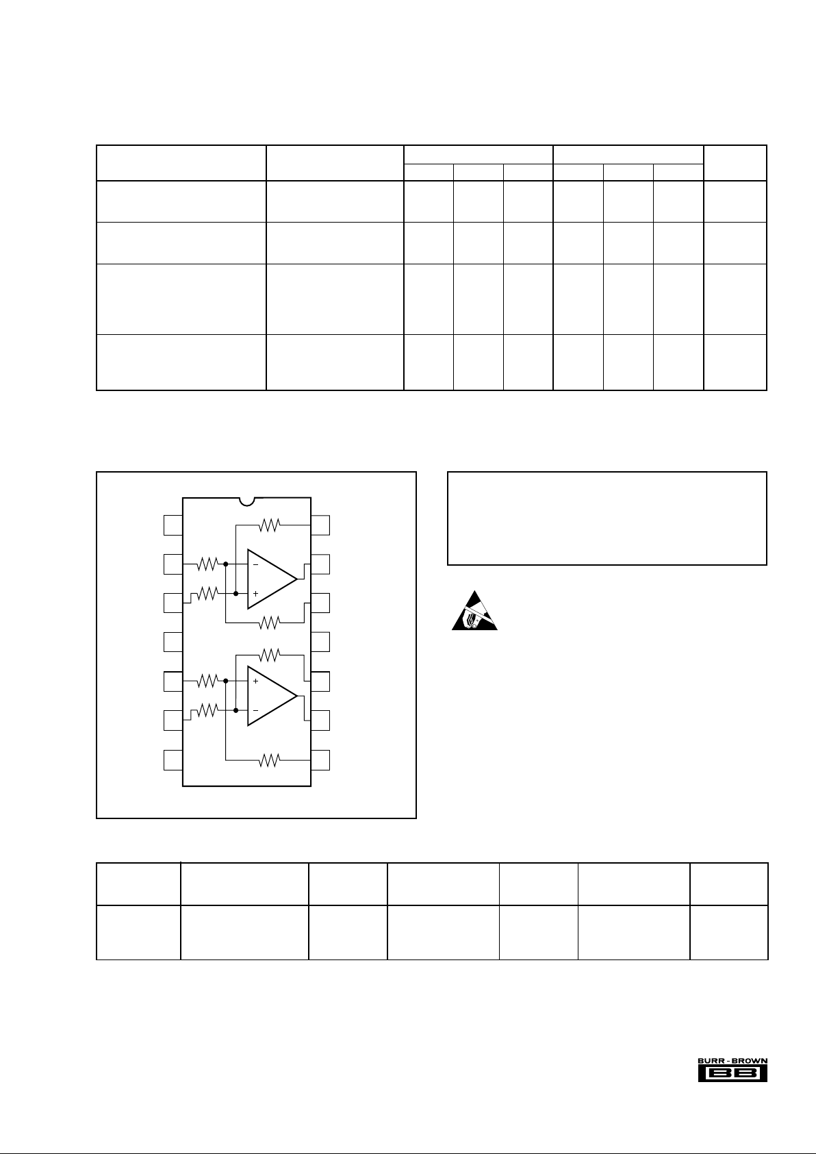
PIN CONFIGURATION
Top View SO-14
Supply Voltage, V+ to V– .................................................................... 36V
Input Voltage Range .......................................................................... ±80V
Output Short-Circuit (to ground) .............................................. Continuous
Operating Temperature .................................................. –55°C to +125°C
Storage Temperature ..................................................... –55°C to +125°C
Junction Temperature .................................................................... +150°C
Lead Temperature (soldering, 10s) ............................................... +300°C
ABSOLUTE MAXIMUM RATINGS
ELECTROSTATIC
DISCHARGE SENSITIVITY
This integrated circuit can be damaged by ESD. Burr-Brown
recommends that all integrated circuits be handled with appropriate precautions. Failure to observe proper handling and
installation procedures can cause damage.
ESD damage can range from subtle performance degradation
to complete device failure. Precision integrated circuits may
be more susceptible to damage because very small parametric
changes could cause the device not to meet its published
specifications.
NC
–In A
+In A
V–
+In B
–In B
NC
Ref A
Out A
Sense A
V+
Sense B
Out B
Ref B
NC = No Connection
1
2
3
4
5
6
7
14
13
12
11
10
9
8
A
B
PACKAGE SPECIFIED
DRAWING TEMPERATURE PACKAGE ORDERING TRANSPORT
PRODUCT PACKAGE NUMBER
(1)
RANGE MARKING NUMBER
(2)
MEDIA
INA2132U SO-14 Surface-Mount 235 –40°C to +85°C INA2132U INA2132U Rails
" " " " " INA2132U/2K5 Tape and Reel
INA2132UA SO-14 Surface-Mount 235 –40°C to +85°C INA2132UA INA2132UA Rails
" " " " " INA2132UA/2K5 Tape and Reel
NOTES: (1) For detailed drawing and dimension table, please see end of data sheet, or Appendix C of Burr-Brown IC Data Book. (2) Models with a slash (/ ) are
available only in Tape and Reel in the quantities indicated (e.g., /2K5 indicates 2500 devices per reel). Ordering 2500 pieces of “INA2132U/2K5” will get a single
2500-piece Tape and Reel. For detailed Tape and Reel mechanical information, refer to Appendix B of Burr-Brown IC Data Book.
PACKAGE/ORDERING INFORMATION
Page 4

4
®
INA2132
TYPICAL PERFORMANCE CURVES
At TA = +25°C and VS = ±15V, unless otherwise noted.
GAIN vs FREQUENCY
Frequency (Hz)
Closed-Loop Gain (dB)
10k 100k 1M
20
0
–20
–40
–60
VS = ±15V or +5V
CL = 100pF
R
L
= 10kΩ
CL = 1000pF
R
L
= ∞
COMMON-MODE REJECTION vs FREQUENCY
Frequency (Hz)
Common-Mode Rejection (dB)
10 100 1k 10k 100k 1M
100
90
80
70
60
50
40
30
VS = ±15V
VS = +5V
CHANNEL SEPARATION vs FREQUENCY
Frequency (Hz)
Channel Separation (dB)
0.1 1 10 1k100 1M100k10k
150
140
130
120
110
100
90
80
70
60
50
OUTPUT VOLTAGE SWING vs OUTPUT CURRENT
V+
(V+) –0.5
(V+) –1
(V+) –1.5
(V+) –2
(V+) –2.5
(V–) +2.5
(V–) +2
(V–) +1.5
(V–) +1
(V–) +0.5
V–
0 ±2 ±4 ±6 ±8 ±10
Output Current (mA)
Output Voltage Swing (V)
125°C
125°C
85°C
–55°C
85°C
85°C
25°C
–40°C
–40°C
25°C
–55°C
QUIESCENT and SHORT-CIRCUIT CURRENT
vs TEMPERATURE
Temperature (°C)
Quiescent Current (µA)
Short-Circuit Current |mA|
–75 –50 –25 0 25 50 75 100 125
210
200
190
180
170
160
150
13
12
11
10
9
8
7
±I
SC
I
Q
POWER SUPPLY REJECTION vs FREQUENCY
Frequency (Hz)
Power Supply Rejection (dB)
10 100 1k 10k 100k 1M
120
100
80
60
40
20
0
VS = ±15V
+PSRR
–PSRR
VS = +5V
Page 5

5
®
INA2132
TYPICAL PERFORMANCE CURVES (CONT)
At TA = +25°C and VS = ±15V, unless otherwise noted.
50mV/div
SMALL-SIGNAL STEP RESPONSE
C
L
= 200pF
50mV/div
10µs/div
SMALL-SIGNAL STEP RESPONSE
C
L
= 1000pF
5V/div
LARGE-SIGNAL STEP RESPONSE
100µs/div
10µs/div
SETTLING TIME vs LOAD CAPACITANCE
Load Capacitance
Settling Time (µs)
100pF 1000pF 10,000pF
100
96
92
88
84
80
0.1%
0.01%
10V Step
INPUT COMMON-MODE VOLTAGE RANGE
vs OUTPUT VOLTAGE
Output Voltage (V)
Common-Mode Voltage (V)
–16 –12 –8 –4 0 4 8 1612
40
30
20
10
0
–10
–20
–30
–40
V
REF
= 0V
G = 1
VS = ±5V
VS = ±15V
VS = +5V
SLEW RATE vs TEMPERATURE
Temperature (°C)
Slew Rate (V/µs)
–75 –50 –25 0 25 50 75 100 125
0.18
0.16
0.14
0.12
0.10
0.08
0.06
Page 6

6
®
INA2132
TYPICAL PERFORMANCE CURVES (CONT)
At TA = +25°C and VS = ±15V, unless otherwise noted.
0.5µV/div
500ms/div
0.1Hz to 10Hz PEAK-TO-PEAK
VOLTAGE NOISE
OFFSET VOLTAGE
PRODUCTION DISTRIBUTION
Percent of Amplifiers (%)
Offset Voltage (µV)
–500
–400
–300
–200
–100
0
100
200
300
400
500
25
20
15
10
5
0
VS = ±15V
OFFSET VOLTAGE
PRODUCTION DISTRIBUTION
Percent of Amplifiers (%)
Offset Voltage (µV)
–700
–600
–500
–400
–300
–200
–100
0
100
200
300
400
500
600
700
18
16
14
12
10
8
6
4
2
0
VS = +5V
OFFSET VOLTAGE DRIFT
PRODUCTION DISTRIBUTION
Percent of Amplifiers (%)
Offset Voltage Drift (µV/°C)
0.511.522.533.544.555.566.577.588.599.5
10
40
35
30
25
20
15
10
5
0
VS = ±15V
Page 7

7
®
INA2132
APPLICATIONS INFORMATION
Figure 1 shows the basic connections required for operation
of the INA2132. Power supply bypass capacitors should be
connected close to the device pins.
The differential input signal is connected to pins 2 and 3 (or
pins 6 and 5) as shown. The source impedances connected to
the inputs must be nearly equal to assure good commonmode rejection. An 8Ω mismatch in source impedance will
degrade the common-mode rejection of a typical device to
approximately 80dB. Gain accuracy will also be slightly
affected. If the source has a known impedance mismatch, an
additional resistor in series with one input can be used to
preserve good common-mode rejection.
Do not interchange pins 3 and 14 (or pins 5 and 8) or pins
2 and 12 (or pins 6 and 10), even though nominal resistor
values are equal. These resistors are laser-trimmed for precise resistor ratios to achieve accurate gain and highest
CMRR. Interchanging these pins may not provide specified
performance. As shown in Figure 1, sense line should be
connected as close to the load as possible.
In the case where V
REF
is grounded, the equation simplifies to:
2 • (V–) < VCM < 2 • ((V+) – 1)
For more information, see the typical performance curve titled
“Input Common-Mode Voltage Range vs Output Voltage.”
OPERATING VOLTAGE
The INA2132 operates from single (+2.7V to +36V) or dual
(±1.35V to ±18V) supplies with excellent performance.
Specifications are production tested with +5V and ±15V
supplies. Most behavior remains unchanged throughout the
full operating voltage range. Parameters which vary significantly with operating voltage are shown in the Typical
Performance Curves.
The INA2132 can accurately measure differential signals
that are beyond the power supply rails. Linear commonmode range extends to twice the negative power supply
voltage and nearly twice the positive power supply voltage.
Output phase reversal does not occur when the inputs to the
internal operational amplifier are overloaded to either rail.
See typical performance curve, “Common-Mode Range vs
Output Voltage.”
OFFSET VOLTAGE TRIM
The INA2132 is laser-trimmed for low offset voltage and
drift. Most applications require no external offset adjustment. Figure 2 shows an optional circuit for trimming the
output offset voltage. The output is referred to the output
reference terminal (pin 14 or pin 8), which is normally
grounded. A voltage applied to the Ref terminal will be
summed with the output signal. This can be used to null
offset voltage. The source impedance of a signal applied to
the Ref terminal should be less than 8Ω to maintain good
common-mode rejection. To assure low impedance at the
Ref terminal, the trim voltage can be buffered with an op
amp, such as the OPA277.
FIGURE 1. Basic Power Supply and Signal Connections.
FIGURE 2. Offset Adjustment.
To ensure valid operation of the differential amplifier, please
note the following points:
1) V
OUT
= V3 – V2 + V
REF
2) V
OUT
must be within the specified linear range. For
example, with ±15V supplies and a 100kΩ load, the
output will be defined by:
(V–) + 0.15V < V
OUT
< (V+) – 0.8V
3) Input common-mode range at the nodes of the op amp
must be V– ≤ VCM ≤ (V+) – 1. To ensure that the inputs
to the differential amp (+In and –In) meet this criteria,
limit the common-mode voltage inputs to:
2 • (V–) – V
REF
< VCM < 2 • ((V+) – 1) – V
REF
V
3
12 (10)
13 (9)
3 (5)
V
O
INA2132
V
O
= V3 – V
2
Offset Adjustment
Range = ±500µV
2 (6)
R
3
Ref
R
1
R
2
R
4
V
2
8Ω
R = 237kΩ
8Ω
100kΩ
+15V
–15V
14 (8)
NOTE: For ±750µV range, R = 158kΩ.
V
3
12 (10)
13 (9)
3 (5)
INA2132
V
OUT
= V3 – V
2
2(6)
R
3
Ref
R
1
R
2
R
4
V
2
40kΩ
40kΩ
40kΩ
40kΩ
R
L
1µF
NOTE: Pin numbers in parentheses ( ) refer to channel B.
V–
4
1µF
V+
11
14 (8)
Page 8

8
®
INA2132
12 (10)
13 (9)
14 (8)
INA2132
ADS7806
(1)
2 (6)
3 (5)
4
11
+5V
–In
12 Bits
Out
0V-4V
Input
+In
τS = 45µs (4V Step to 0.01%)
NOTE: (1) For 16-bit output, use ADS7809.
FIGURE 4. Differential Input Voltage-to-Current Converter
for Low I
OUT
.
FIGURE 5. Differential Input Data Acquisition.
FIGURE 3. Low Power, High Output Current Precision
Difference Amplifier.
CAPACITIVE LOAD DRIVE CAPABILITY
The INA2132 can drive large capacitive loads, even at low
supplies. It is stable with a 10nF load. Refer to the “SmallSignal Step Response” and “Settling Time vs Load Capacitance” typical performance curves.
CHANNEL CROSSTALK
The two channels of the INA2132 are completely independent, including all bias circuitry. At dc and low frequency,
there is virtually no signal coupling between channels.
Crosstalk increases with frequency and is dependent on
source impedance and signal characteristics. See the typical
performance curve “Channel Separation vs Frequency” for
more information.
Most crosstalk is produced by capacitive coupling of signals
from one channel to the input section of the other channel.
To minimize coupling, separate the input traces as far as
practical from any signals associated with the opposite
channel. A grounded guard trace surrounding the inputs
helps reduce stray coupling between channels. Run the
differential inputs of each channel parallel to each other or
directly adjacent on the top and bottom sides of a circuit
board. Stray coupling then produces a common-mode signal
which is rejected by the INA2132’s input.
12 (10)
13 (9)
14 (8)
INA2132
BUF634
2 (6)
3 (5)
V
O
R
L
–In
+In
(Low IQ mode)
BUF634 inside feedback
loop contributes no error.
12 (10)
13 (9)
3 (5)
INA2132
2 (6)
14 (8)
V
3
V
2
Load
I
O
= (V3 – V2)/R
I
O
R
12 (10)
13 (9)
3 (5)
14 (8)
INA2132
2 (6)
1
V
O
DG188
V
1
Logic
In
Logic In
0
1
V
O
–V
1
+V
1
FIGURE 6. Digitally Controlled Gain of ±1 Amplifier.
FIGURE 7. Precision Voltage-to-Current Converter with
Differential Inputs.
12 (10)
13 (9)
3 (5)
INA2132
2 (6)
14 (8)
V
1
V
2
Load
IO = (V1 – V2) (1/40k + 1/R)
I
O
R
R
Page 9

9
®
INA2132
12
13
3
INA2132
A
B
2
V
01
14
10
9
5
6
V
01
– V
02
= 2 (V2 – V1)
V
02
8
V
2
V
1
FIGURE 8. Differential Output Difference Amplifier.
FIGURE 10. Precision Instrumentation Amplifier.
12
13
3
INA2132
2
V
01
14
10
9
5
6
V
01
= (V3 – V2) +
8
V
3
V
LS
Level-Shift
Voltage
Reference
V
2
V
LS
2
A
B
FIGURE 9. Precision Level Shifter.
12 (10)
13 (9)
14 (8)
3 (5)
INA2132
2 (6)
V
1
V
O
A
2
A
1
R
2
R
2
R
1
–In
V
2
+In
VO = (1 + 2R2/R1) (V2 –V1)
The INA2132 can be combined with op amps to form
a complete instrumentation amplifier with specialized
performance characteristics. Burr-Brown offers many
complete high performance IAs. Products with similar
performances are shown below.
OPA227 Low Noise INA103
OPA129 Ultra-Low Bias Current (fA) INA116
OPA2277 Low Offset Drift, Low Noise INA114, INA128
OPA2130 Low Power, FET-Input (pA) INA121
OPA2234, OPA2241, OPA2244 Single Supply, Precision, Low Power INA122, INA118
OPA2237 Single Supply, Low Power, MSOP-8 INA122, INA126
SIMILAR COMPLETE
A
1
, A
2
FEATURES BURR-BR0WN IAs
Page 10

10
®
INA2132
12 (10)
13 (9)
V
0
INA2132
V0 = – V
2
2 (6)
V
2
3 (5) 14 (8)
V
3
12 (10)
13 (9)
3 (5)
2 (6)
INA2132
14 (8)
V
0
V0 = V3/2
= 1/2 V
3
V
1
12 (10)
13 (9)
3 (5)
14 (8)
2 (6)
V
0
INA2132
V
0
= (V1 + V3)/2
V
3
V
1
12 (10)
13 (9)
3 (5)
14 (8)
2 (6)
V
0
INA2132
V
0
= V
1
V
1
12 (10)
13 (9)
3 (5)
14 (8)
V
0
INA2132
V
0
= 2 • V
1
2 (6)
V
1
12 (10)
13 (9)
3 (5)
14 (8)
V
0
INA2132
V
0
= V1 + V
3
2 (6)
V
3
FIGURE 11. Precision Inverting Unity-Gain Amplifier.
FIGURE 12. Precision Gain = 1/2 Amplifier.
FIGURE 13. Precision Average Value Amplifier.
FIGURE 14. Precision Unity-Gain Buffer.
FIGURE 15. Precision Gain = 2 Amplifier.
FIGURE 16. Precision Summing Amplifier.
 Loading...