

Page 1
High-Speed, Precision
DIFFERENCE AMPLIFIER
©1999 Burr-Brown Corporation PDS-1483B Printed in U.S.A. March, 1999
®
FEATURES
● DESIGNED FOR LOW COST
● LOW OFFSET VOLTAGE: ±500µV max
● LOW OFFSET DRIFT: ±2µV/°C
● LOW GAIN ERROR: ±0.05% max
● WIDE BANDWIDTH: 3MHz
● HIGH SLEW RATE: 14V/µs
● FAST SETTLING TIME: 3µs to 0.01%
● WIDE SUPPLY RANGE: ±4V to ±18V
● LOW QUIESCENT CURRENT: 2.4mA
● SO-8 SURFACE-MOUNT PACKAGE
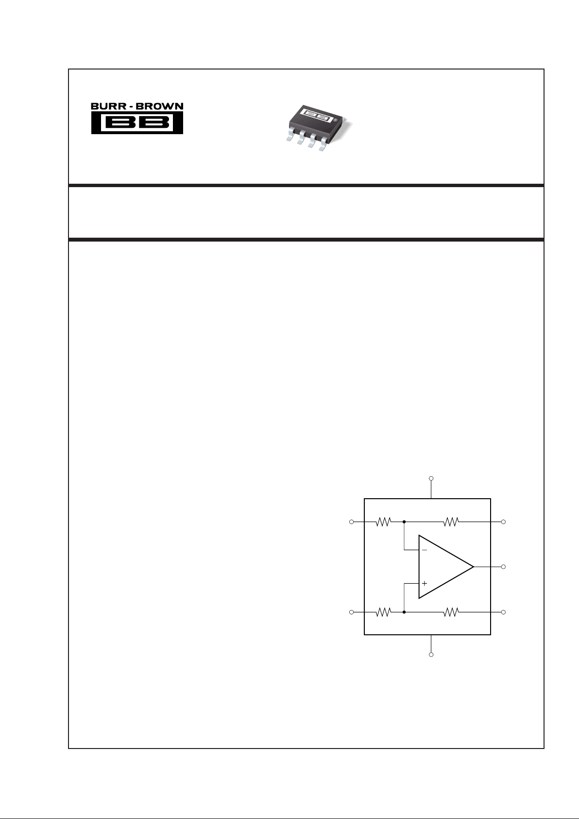
INA157
DESCRIPTION
The INA157 is a high slew rate, G = 1/2 or G = 2
difference amplifier consisting of a precision op amp
with a precision resistor network. The on-chip resistors are laser trimmed for accurate gain and high
common-mode rejection. Excellent TCR tracking of
the resistors maintains gain accuracy and commonmode rejection over temperature. The input commonmode voltage range extends beyond the positive and
negative supply rails. It operates on ±4V to ±18V
supplies.
The difference amplifier is the foundation of many
commonly used circuits. The INA157 provides this
circuit function without using an expensive precision
resistor network. The INA157 is available in a SO-8
surface-mount package and is specified for operation
over the extended industrial temperature range, –40°C
to +85°C.
APPLICATIONS
● DIFFERENTIAL INPUT AMPLIFIER
● INSTRUMENTATION AMPLIFIER
BUILDING BLOCK
● G = 1/2 AMPLIFIER
● G = 2 AMPLIFIER
● DIFFERENTIAL CURRENT RECEIVER
● VOLTAGE-CONTROLLED CURRENT SOURCE
● GROUND LOOP ELIMINATOR
● CURRENT SHUNT MONITOR
International Airport Industrial Park • Mailing Address: PO Box 11400, Tucson, AZ 85734 • Street Address: 6730 S. Tucson Blvd., Tucson, AZ 85706 • Tel: (520) 746-1111
Twx: 910-952-1111 • Internet: http://www.burr-brown.com/ • Cable: BBRCORP • Telex: 066-6491 • FAX: (520) 889-1510 • Immediate Product Info: (800) 548-6132
2
3
4
–In
+In
V–
6kΩ12kΩ
6kΩ12kΩ
5
1
Sense
Ref
6
Output
7
V+
INA157
For most current data sheet and other product
information, visit www.burr-brown.com
Page 2
2
®
INA157
SPECIFICATIONS: VS = ±15V
At TA = +25°C, VS = ±15V, RL = 2kΩ connected to ground, and reference pin connected to ground, unless otherwise noted.
The information provided herein is believed to be reliable; however, BURR-BROWN assumes no responsibility for inaccuracies or omissions. BURR-BROWN assumes
no responsibility for the use of this information, and all use of such information shall be entirely at the user’s own risk. Prices and specifications are subject to change
without notice. No patent rights or licenses to any of the circuits described herein are implied or granted to any third party. BURR-BROWN does not authorize or warrant
any BURR-BROWN product for use in life support devices and/or systems.
INA157U INA157UA
PARAMETER CONDITIONS MIN TYP MAX MIN TYP MAX UNITS
OFFSET VOLTAGE
(1)
RTO
Initial
(1)
±100 ±500 ✽ ±1000 µV
vs Temperature ±2 ±20 ✽✽µV/°C
vs Power Supply V
S
= ±4V to ±18V ±5 ±60 ✽✽µV/V
vs Time 0.25 ✽ µV/mo
INPUT IMPEDANCE
(2)
Differential 24 ✽ kΩ
Common-Mode 18 ✽ kΩ
INPUT VOLTAGE RANGE
Common-Mode Voltage Range
Positive VO = 0V 3(V+)–7.5 3(V+)–6 ✽✽ V
Negative VO = 0V 3(V–)+7.5 3(V–)+3 ✽✽ V
Common-Mode Rejection Ratio
VCM = –37.5V to 37.5V, RS = 0Ω
86 96 80 ✽ dB
OUTPUT VOLTAGE NOISE
(3)
RTO
f = 0.1Hz to 10Hz 1.3 ✽ µVp-p
f = 1kHz 26 ✽ nV/√Hz
GAIN
Initial 0.5 ✽ V/V
Error V
O
= –10V to +10V ±0.01 ±0.05 ✽ ±0.1 %
vs Temperature ±1 ±10 ✽✽ppm/°C
Nonlinearity VO = –10V to +10V ±0.0001 ±0.001 ✽ ±0.002 % of FS
OUTPUT
Voltage, Positive (V+)–2 (V+)–1.8 ✽✽ V
Negative (V–)+2 (V–)+1.6 ✽✽ V
Current Limit, Continuous to Common ±60 ✽ mA
Capacitive Load (stable operation) 500 ✽ pF
FREQUENCY RESPONSE
Small-Signal Bandwidth –3dB 4 ✽ MHz
Slew Rate 14 ✽ V/µs
Settling Time: 0.1% 10V Step, C
L
= 100pF 2 ✽ µs
0.01% 10V Step, CL = 100pF 3 ✽ µs
Overload Recovery Time 50% Overdrive 3 ✽ µs
POWER SUPPLY
Rated Voltage ±15 ✽ V
Operating Voltage Range ±4 ±18 ✽✽V
Quiescent Current IO = 0mA ±2.4 ±2.9 ✽✽mA
TEMPERATURE RANGE
Specified –40 +85 ✽✽°C
Operation –55 +125 ✽✽°C
Storage –55 +125 ✽✽°C
Thermal Resistance,
Θ
JA
SO-8 Surface-Mount 150 ✽ °C/W
✽Specifications the same as INA157U.
NOTES: (1) Includes effects of amplifier’s input bias and offset currents. (2) Internal resistors are ratio matched but have ±20% absolute value. (3) Includes effects
of amplifier’s input current noise and thermal noise contribution of resistor network.
Page 3
3
®
INA157
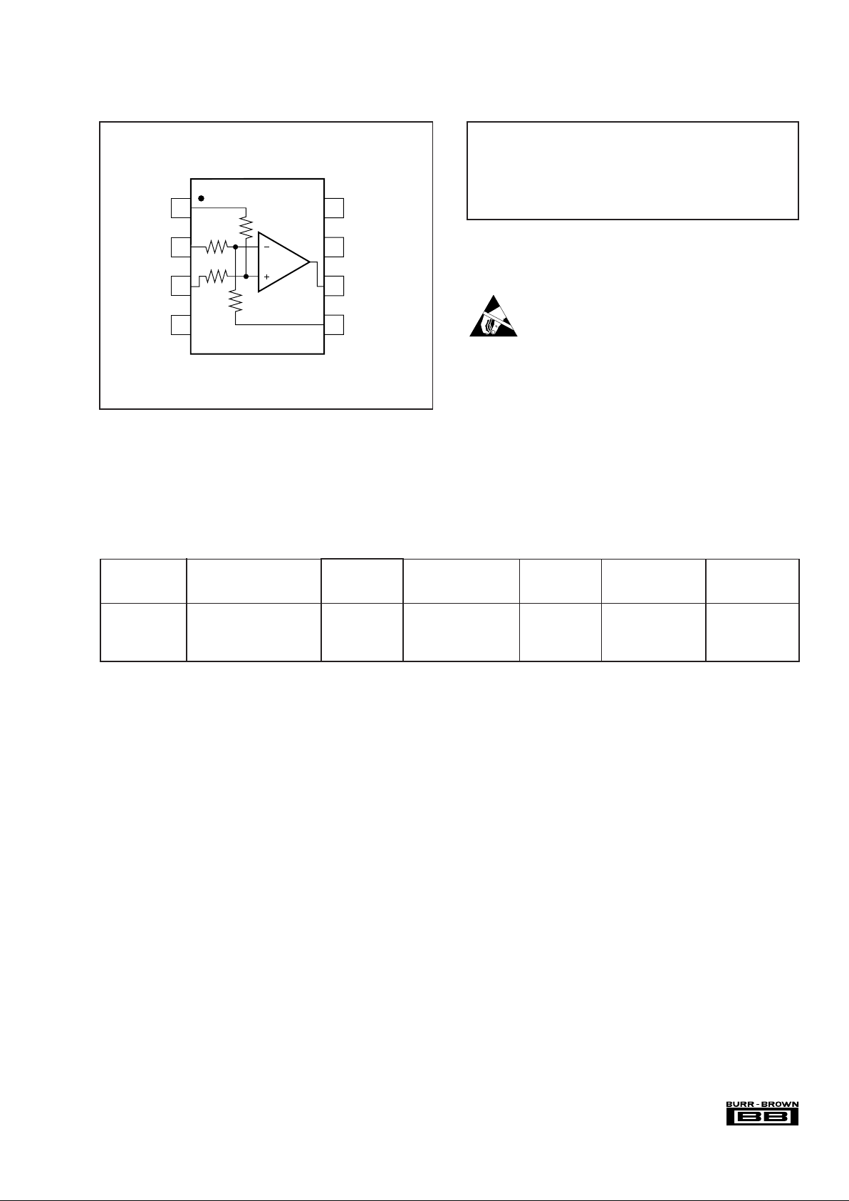
PIN CONFIGURATION
TOP VIEW SO-8
Supply Voltage, V+ to V– .................................................................... 40V
Input Voltage Range .......................................................................... ±80V
Output Short Circuit (to ground) ............................................. Continuous
Operating Temperature .................................................. –55°C to +125°C
Storage Temperature ..................................................... –55 °C to +125°C
Junction Temperature .................................................................... +150°C
Lead Temperature (soldering, 10s) ............................................... +300°C
NOTE: (1) Stresses above these ratings may cause permanent damage.
Exposure to absolute maximum conditions for extended periods may degrade
device reliability.
ABSOLUTE MAXIMUM RATINGS
(1)
ELECTROSTATIC
DISCHARGE SENSITIVITY
This integrated circuit can be damaged by ESD. Burr-Brown
recommends that all integrated circuits be handled with appropriate precautions. Failure to observe proper handling and
installation procedures can cause damage.
ESD damage can range from subtle performance degradation
to complete device failure. Precision integrated circuits may
be more susceptible to damage because very small parametric
changes could cause the device not to meet its published
specifications.
PACKAGE SPECIFIED
DRAWING TEMPERATURE PACKAGE ORDERING TRANSPORT
PRODUCT PACKAGE NUMBER
(1)
RANGE MARKING NUMBER
(2)
MEDIA
INA157U SO-8 Surface-Mount 182 –40°C to +85°C INA157U INA157U Rails
"""""INA157U/2K5 Tape and Reel
INA157UA SO-8 Surface-Mount 182 –40°C to +85°C INA157UA INA157UA Rails
"""""INA157UA/2K5 Tape and Reel
NOTES: (1) For detailed drawing and dimension table, please see end of data sheet, or Appendix C of Burr-Brown IC Data Book. (2) Models with a slash (/ ) are
available only in Tape and Reel in the quantities indicated (e.g., /2K5 indicates 2500 devices per reel). Ordering 2500 pieces of “INA157U/2K5” will get a single
2500-piece Tape and Reel. For detailed Tape and Reel mechanical information, refer to Appendix B of Burr-Brown IC Data Book.
PACKAGE/ORDERING INFORMATION
Ref
–In
+In
V–
NC
V+
Output
Sense
NC = No Connection
1
2
3
4
8
7
6
5
Page 4

4
®
INA157
TYPICAL PERFORMANCE CURVES
At TA = +25°C, VS = ±15V, and G = 1/2, unless otherwise noted.
GAIN vs FREQUENCY
Frequency (Hz)
Voltage Gain (dB)
1k 10k 100k 1M 10M
10
0
–10
–20
–30
COMMON-MODE REJECTION RATIO vs FREQUENCY
Frequency (Hz)
Common-Mode Rejection Ratio (dB)
1k 10k 100k 1M
100
80
60
40
RTO
POWER SUPPLY REJECTION RATIO vs FREQUENCY
Frequency (Hz)
Power Supply Rejection (dB)
100 1k 10k 100k 1M
120
100
80
60
40
20
0
–PSRR
RTO
+PSRR
MAXIMUM OUTPUT VOLTAGE vs FREQUENCY
Frequency (Hz)
Output Voltage (Vp-p)
100 1k 10k 100k 1M 10M
40
30
20
10
0
INPUT COMMON-MODE VOLTAGE
vs OUTPUT VOLTAGE
Output Voltage (V)
Common-Mode Voltage (V)
–20 –15 –10 –5 0 5 10 15 20
80
60
40
20
0
–20
–40
–60
–80
V
REF
= 0V
R
L
= 2kΩ
G = 1/2
V
S
= ±15V
TOTAL HARMONIC DISTORTION + NOISE
vs FREQUENCY
Frequency (Hz)
THD+Noise (%)
20 100 1k 10k 20k
0.1
0.010
0.001
0.0001
VO = 5Vrms
RL = 600Ω
RL = 100kΩ
RL = 2kΩ
Page 5

5
®
INA157
TYPICAL PERFORMANCE CURVES (CONT)
At TA = +25°C, VS = ±15V, and G = 1/2, unless otherwise noted.
QUIESCENT CURRENT vs TEMPERATURE
Temperature (°C)
Quiescent Current (mA)
–75 –50 –25 0 25 50 75 100 125
4
3
2
1
0
SLEW RATE vs TEMPERATURE
Temperature (°C)
Slew Rate (V/µs)
–75 –50 –25 0 25 50 75 100
+SR
125
16
14
12
10
8
–SR
OUTPUT VOLTAGE NOISE SPECTRAL DENSITY
vs FREQUENCY
Frequency (Hz)
Voltage Noise (nV/√Hz)
1 10 100 1k 10k 100k 1M
10k
1k
100
10
OUTPUT NOISE VOLTAGE
vs NOISE BANDWIDTH
Frequency (Hz)
Noise Voltage (µVrms)
1 10 100 1k 10k 100k
100
10
1
0.1
SHORT-CIRCUIT CURRENT vs TEMPERATURE
Temperature (°C)
Short-Circuit Current (mA)
–75 –50 –25 0 25 50 75 100 125
80
60
40
20
0
–20
–40
–60
–80
+I
SC
–I
SC
OUTPUT VOLTAGE SWING vs OUTPUT CURRENT
14
13
12
11
10
9
–9
–10
–11
–12
–13
–14
0 ±20 ±40 ±60 ±80
Output Current (mA)
Output Voltage Swing (V)
–55°C
–55°C
25°C
85°C
85°C
125°C
125°C
25°C
Page 6

6
®
INA157
TYPICAL PERFORMANCE CURVES (CONT)
At TA = +25°C, VS = ±15V, and G = 1/2, unless otherwise noted.
SMALL-SIGNAL STEP RESPONSE
1µs/div
50mV/div
LARGE-SIGNAL STEP RESPONSE
1µs/div
5V/div
CL = 100pF
C
L
= 500pF
SMALL-SIGNAL OVERSHOOT
vs LOAD CAPACITANCE
Load Capacitance (pF)
Overshoot (%)
0 200 400 600 800 1000 1200
70
60
50
40
30
20
10
0
RL = 2kΩ
100mV Step
OFFSET VOLTAGE
PRODUCTION DISTRIBUTION
Percent of Units (%)
Offset Voltage (µV)
–1000
–900
–800
–700
–600
–500
–400
–300
–200
–100
0
100
200
300
400
500
600
700
800
900
1000
35
30
25
20
15
10
5
0
Typical Production
Distribution of
Packaged Units.
OFFSET VOLTAGE DRIFT
PRODUCTION DISTRIBUTION
Percent of Units (%)
Offset Voltage Drift (µV/°C)
1 2 3 4 5 6 7 8 9 10 11 12 13 14 15 16 17 18 19 20
25
20
15
10
5
0
Typical production distribution
of packaged units.
CL = 500pF
Page 7

7
®
INA157
APPLICATIONS INFORMATION
The INA157 is a difference amplifier suitable for a wide
range of general-purpose applications. Figure 1 shows the
basic G = 1/2 configuration. The input and feedback resistors can be reversed to achieve G = 2, as shown in Figure 2.
For applications requiring G = 1, the INA154 is recommended.
Decoupling capacitors are strongly recommended for applications with noisy or high impedance power supplies. The
capacitors should be placed close to the device pins as
shown in Figure 1.
As shown in Figure 1, the output is referred to the reference
terminal (pin 1). A voltage applied to this pin will be
summed with the output signal. The differential input signal
is connected to pins 2 and 3. The source impedances connected to the inputs must be nearly equal to assure good
common-mode rejection. A 5Ω mismatch in source impedance will degrade the common-mode rejection of a typical
device to approximately 77dB (RTO). If the source has a
known impedance mismatch, an additional resistor in series
with the opposite input can be used to preserve good common-mode rejection.
V
3
5
6
3
1
Ref
INA157
V
O
= 1/2 (V3 – V2)
2
R
3
12kΩ
R
1
12kΩ
R
2
6kΩ
R
4
6kΩ
R
L
V
2
–In
+In
1µF
V–
4
1µF
V+
7
FIGURE 1. G = 1/2 Differential Amplifier (basic power
supply and signal connections).
FIGURE 2. G = 2 Differential Amplifier.
V
3
5
6
3
V
O
INA157
V
O
= 1/2 (V3 – V2)
Offset Adjustment
Range = ±1mV
G = 1/2
2
R
4
6kΩ
V
2
20Ω
250kΩ
10Ω
100kΩ
+15V
–15V
1
R
3
12kΩ
R
1
12kΩ
R
2
6kΩ
FIGURE 3. Offset Adjustment.
OPERATING VOLTAGE
The INA157 operates from ±4V to ±18V supplies with
excellent performance. Most behavior remains unchanged
throughout the full operating voltage range. Parameters
which vary significantly with operating voltage are shown in
the Typical Performance Curves.
INPUT VOLTAGE RANGE
The INA157 can accurately measure differential signals
that are above the positive or negative power supply rail. In
a gain of 1/2, the linear common-mode range extends from
3•(V+) – 7.5V to 3•(V–) +7.5V. See the Typical Performance Curve, “Input Common-Mode Range vs Output
Voltage.”
OFFSET VOLTAGE TRIM
The INA157 is laser trimmed for low offset voltage and
drift. Most applications require no external offset adjustment. Figure 3 shows an optional circuit for trimming the
output offset voltage. The output is referred to the output
reference terminal (pin 1), which is normally grounded. A
voltage applied to the Ref terminal will be summed with the
output signal. This can be used to null offset voltage as
shown in Figure 3. The source impedance of a signal
applied to the Ref terminal should be less than 10Ω to
maintain good common-mode rejection.
V
3
2
6
1
INA157
V
O
= 2 (V3 – V2)
5
R
4
6kΩ
R
3
12kΩ
R
2
6kΩ
R
1
12kΩ
V
2
–In
+In
3
Ref
R
L
Page 8

8
®
INA157
The INA157 can be combined with op amps to form a complete instrumentation amplifier with specialized performance characteristics. BurrBrown offers many complete high performance IAs. Products with related
performances are shown at the right.
SIMILIAR COMPLETE
A
1
, A
2
FEATURE BURR-BROWN IAs
OPA227 Low Noise INA103
OPA129 Ultra Low Bias Current (fA) INA116
OPA277 Low Offset Drift, Low Noise INA114, INA128
OPA2134 FET Input (pA) INA111, INA121
FIGURE 6. Boosting Output Current.
FIGURE 5. Precision Instrumentation Amplifier.
FIGURE 4. Precision Summing Amplifier.
V
1
V
2
5
6
1
3
V0 = 2V1 + V
2
INA157
2
6kΩ
6kΩ
12kΩ
12kΩ
5
6
1
3
INA157
2
V
1
V
O
A
2
A
1
R
2
R
2
R
1
–In
V
2
+In
VO = (1 + 2R2/R1) (V2 –V1)
5
6
1
INA157
BUF634
2
3
V
O
R
L
–In
+In
(Low IQ mode)
BUF634 inside feedback
loop contributes no error.
The difference amplifier is a highly versatile building
block that is useful in a wide variety of applications. See
the INA105 data sheet for additional applications ideas,
including:
• Current Receiver with Compliance to Rails
• ±10V Precision Voltage Reference
• ±5V Precision Voltage Reference
• Precision Average Value Amplifier
• Precision Bipolar Offsetting
• Precision Summing Amplifier with Gain
• Instrumentation Amplifier Guard Drive Generator
• Precision Summing Instrumentation Amplifier
• Precision Absolute Value Buffer
• Precision Voltage-to-Current Converter with Differential
Inputs
• Differential Input Voltage-to-Current Converter for Low
I
OUT
• Isolating Current Source
• Differential Output Difference Amplifier
• Isolating Current Source with Buffering Amplifier for
Greater Accuracy
• Window Comparator with Window Span and Window
Center Inputs
• Precision Voltage-Controlled Current Source with Buffered Differential Inputs and Gain
• Digitally Controlled Gain of ±1 Amplifier
 Loading...