

Page 1
1
®
INA146
®
INA146
©1999 Burr-Brown Corporation PDS-1491A Printed in U.S.A. September, 1999
High-Voltage, Programmable Gain
DIFFERENCE AMPLIFIER
International Airport Industrial Park • Mailing Address: PO Box 11400, Tucson, AZ 85734 • Street Address: 6730 S. Tucson Blvd., Tucson, AZ 85706 • Tel: (520) 746-1111
Twx: 910-952-1111 • Internet: http://www.burr-brown.com/ • Cable: BBRCORP • Telex: 066-6491 • FAX: (520) 889-1510 • Immediate Product Info: (800) 548-6132
For most current data sheet and other product
information, visit www.burr-brown.com
INA146
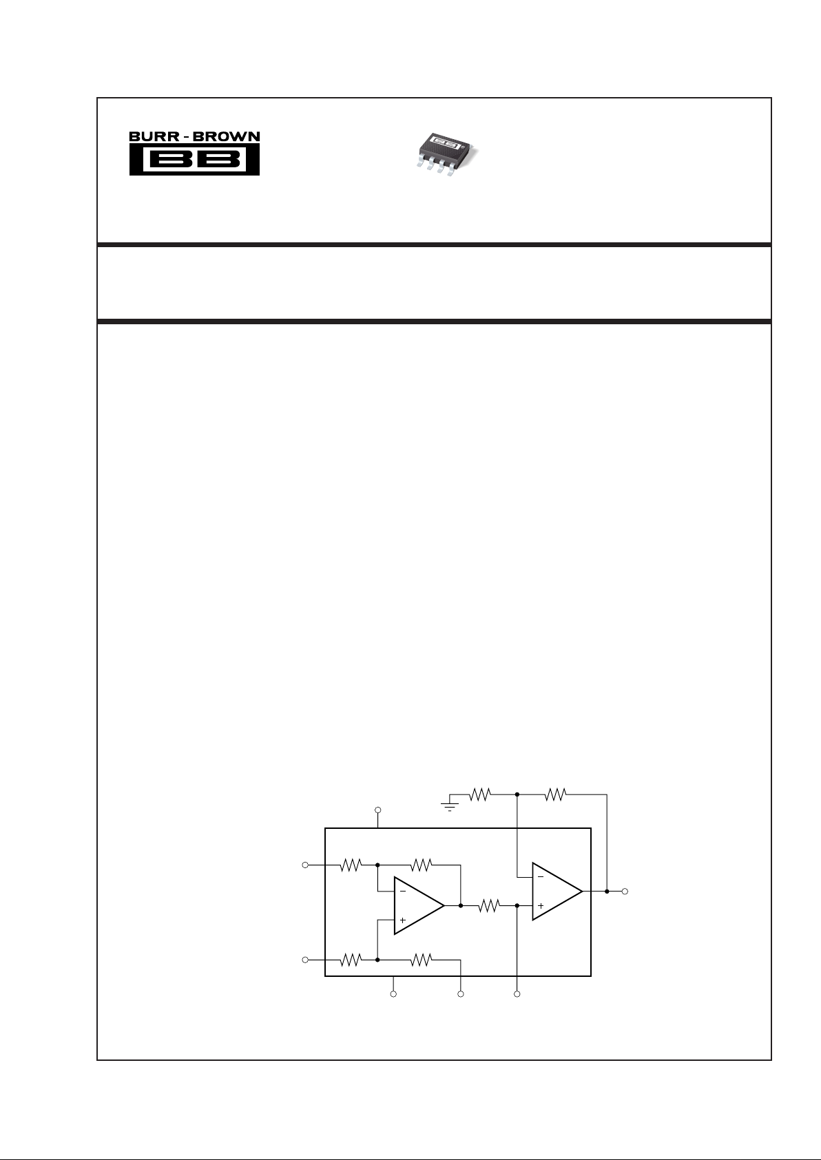
DESCRIPTION
The INA146 is a precision difference amplifier that
can be used to accurately attenuate high differential
voltages and reject high common-mode voltages for
compatibility with common signal processing voltage
levels. High-voltage capability also affords inherent
input protection. The input common-mode range extends beyond both supply rails, making the INA146
well-suited for both single and dual supply applications.
On-chip precision resistors are laser-trimmed to achieve
accurate gain and high common-mode rejection. Excellent TCR tracking of these resistors assures continued high precision over temperature.
A 10:1 difference amplifier provides 0.1V/V gain
when the output amplifier is used as a unity-gain
buffer. In this configuration, input voltages up to
±100V can be measured. Gains greater than 0.1V/V
can be set with an external resistor pair without affecting the common-mode input range.
The INA146 is available in the SO-8 surface-mount
package specified for the extended industrial temperature range, –40°C to +85°C.
FEATURES
● HIGH COMMON-MODE VOLTAGE:
+40V at VS = +5V
±100V at V
S
= ±15V
● DIFFERENTIAL GAIN = 0.1V/V TO 100V/V:
Set with External Resistors
● LOW QUIESCENT CURRENT: 570µA
● WIDE SUPPLY RANGE:
Single Supply: 4.5V to 36V
Dual Supplies: ±2.25V to ±18V
● LOW GAIN ERROR: 0.025%
● HIGH CMR: 80dB
● SO-8 PACKAGE
APPLICATIONS
● CURRENT SHUNT MEASUREMENTS
● SENSOR AMPLIFIER
● SYNCHRONOUS DEMODULATOR
●
CURRENT AND DIFFERENTIAL LINE
RECEIVER
● VOLTAGE-CONTROLLED CURRENT
SOURCE
● BATTERY POWERED SYSTEMS
● LOW COST AUTOMOTIVE
INSTRUMENTATION
R
5
10kΩ
(1%)
A1
V
IN
INA146
V
O
R
2
10kΩ
R
1
100kΩ
V
IN
R
3
100kΩ
R
4
10kΩ
R
G1
R
G2
A2
V
01
RefV–
V+
G = 0.1
+
–
2
5
7
418
6
3
V
O
= (VIN – VIN) 0.1 (1 + RG2/RG1)
+–
Page 2
2
®
INA146
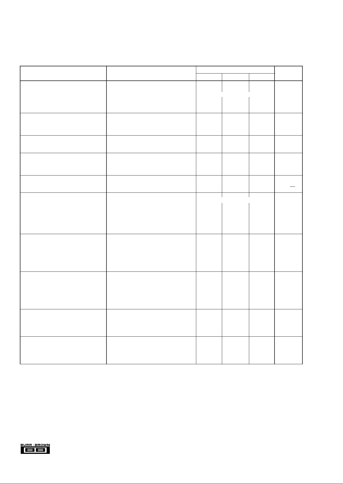
SPECIFICATIONS: VS = ±2.25V to ±18V Dual Supplies
At TA = +25°C, G = 0.1, RL = 10kΩ connected to ground and ref pin connected to ground unless otherwise noted.
Boldface limits apply over the specified temperature range, T
A
= –40°C to +85°C.
The information provided herein is believed to be reliable; however, BURR-BROWN assumes no responsibility for inaccuracies or omissions. BURR-BROWN assumes
no responsibility for the use of this information, and all use of such information shall be entirely at the user’s own risk. Prices and specifications are subject to change
without notice. No patent rights or licenses to any of the circuits described herein are implied or granted to any third party. BURR-BROWN does not authorize or warrant
any BURR-BROWN product for use in life support devices and/or systems.
INA146UA
PARAMETER CONDITION MIN TYP MAX UNITS
OFFSET VOLTAGE, V
O
RTI
(1, 2)
Input Offset Voltage V
OS
VS = ±15, V
CM
= VO = 0V ±1 ±5mV
vs Temperature ∆V
OS
/∆T See Typical Curve
vs Power Supply PSRR V
S
= ±1.35V to ±18V ±100 ±600 µV/V
vs Time ±3 µV/mo
Offset Voltage, V
01
RTI
(1, 2)
±1mV
INPUT VOLTAGE RANGE
Common-Mode Voltage Range V
CM
(VIN+) – (VIN–) = 0V, VO = 0V ±100
(3)
V
Common-Mode Rejection CMRR V
CM
= 11 (V–) to 11 (V+) = 11, RS = 0Ω 70 80 dB
Over Temperature 64 74 dB
INPUT BIAS CURRENT
(2)
VCM = VS/2
Bias Current I
B
±50 nA
Offset Current I
OS
±5nA
INPUT IMPEDANCE
Differential (non-inverting input) 110 kΩ
Differential (inverting input) 91.7 kΩ
Common-Mode 55 kΩ
NOISE RTI
(1, 4)
Voltage Noise, f = 0.1Hz to 10Hz 10 µVp-p
Voltage Noise Density, f = 1kHz e
n
550 nV/√Hz
GAIN
G = 0.1 to 100
Gain Equation G = 0.1 • (1 + RG2/RG1)V/V
Initial
(1)
0.1 V/ V
Gain Error R
L
= 100kΩ, VO = (V–)+0.15 to (V+)–1, G = 1 ±0.025 ±0.1 %
vs Temperature R
L
= 100kΩ, VO = (V–)+0.25 to (V+)–1, G = 1 ±1 ±10 ppm/°C
R
L
= 10kΩ, VO = (V–)+0.3 to (V+)–1.25, G = 1 ±0.025 ±0.1 %
vs Temperature R
L
= 10kΩ, VO = (V–)+0.5 to (V+)–1.25, G = 1 ±1 ±10 ppm/°C
Nonlinearity V
O
= (V–)+0.3 to (V+)–1.25, G = 1 ±0.001 ±0.01 % of FS
FREQUENCY RESPONSE
Small Signal Bandwidth G = 0.1 550 kHz
G = 1 50 kHz
Slew Rate 0.45 V/µs
Settling Time, 0.1% G = 1, 10V Step 40 µs
0.01% G = 1, 10V Step 80 µs
Overload Recovery 50% Input Overload 40 µs
OUTPUT, V
O
Voltage Output RL = 100kΩ, G = 1 (V–) + 0.15 (V+) – 1 V
Over Temperature R
L
= 100kΩ, G = 1 (V–) + 0.25 (V+) – 1 V
R
L
= 10kΩ, G = 1 (V–) + 0.3 (V+) – 1.25 V
Over Temperature R
L
= 10kΩ, G = 1 (V–) + 0.5 (V+) – 1.25 V
Short-Circuit Current Continuous to Common ±15 mA
Capacitive Load Stable Operation 1000 pF
POWER SUPPLY
Specified Voltage Range, Dual Supplies ±2.25 ±18 V
Operating Voltage Range ±1.35 ±18 V
Quiescent Current V
IN
= 0, IO = 0 ±570 ±700 µA
Over Temperature
±750 µA
TEMPERATURE RANGE
Specified Range –40 +85 °C
Operating Range –55 +125 °C
Storage Range –55 +125 °C
Thermal Resistance
θ
JA
150 °C/W
NOTES: (1) Overall difference amplifier configuration. Referred to input pins (V
IN
+ and VIN–), gain = 0.1V/V. Specified with 10kΩ in feedback of A2. (2) Input offset
voltage specification includes effects of amplifier’s input bias and offset currents. (3) Common-mode voltage range is 11 (V–) to 11 [(V+) – 1] with a maximum of ±100V.
(4) Includes effects of input current noise and thermal noise contribution of resistor network.
Page 3
3
®
INA146
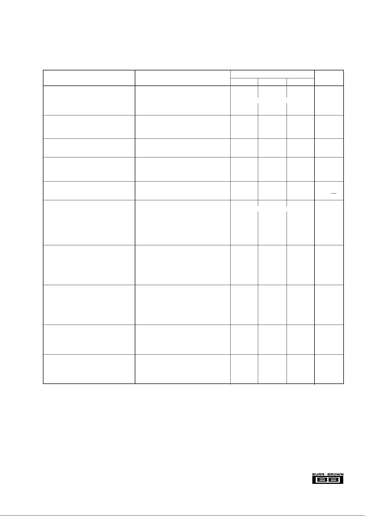
SPECIFICATIONS: VS = +5V Single Supply
At TA = +25°C, G = 1, RL = 10kΩ connected to VS/2 and Ref pin connected to VS/2 unless otherwise noted.
Boldface limits apply over the specified temperature range, T
A
= –40°C to +85°C.
INA146UA
PARAMETER CONDITION MIN TYP MAX UNITS
OFFSET VOLTAGE, V
O
RTI
(1, 2)
Input Offset Voltage V
OS
V
CM
= VO = 0V ±3 ±10 mV
vs Temperature ∆V
OS
/∆T See Typical Curve
vs Power Supply Rejection Ratio PSRR V
S
= ±1.35V to ±18V ±100 ±600 µV/°C
vs Time ±3 µV/mo
INPUT VOLTAGE RANGE
Common-Mode Voltage Range V
CM
VIN+ – VIN– = 0V, VO = 0V –25 19 V
Common-Mode Rejection Ratio CMRR V
CM
= –25V to +19V, RS = 0Ω 70 80 dB
Over Temperature 64 74 dB
INPUT BIAS CURRENT
(2)
Bias Current I
B
±50 nA
Offset Current I
OS
±5nA
INPUT IMPEDANCE
Differential (non-inverting input) 110 kΩ
Differential (inverting input) 91.7 kΩ
Common-Mode 55 kΩ
NOISE RTI
(1, 3, 4)
Voltage Noise, f = 0.1Hz to 10Hz 10 µVp-p
Voltage Noise Density, f = 1kHz e
n
550 nV/√Hz
GAIN
G = 0.1 to 100
V/V
Gain Equation G = 0.1 • (1 + R
G2/RG1
)V/V
Initial
(1)
0.1 V/ V
Gain Error R
L
= 100kΩ, VO = 0.15V to 4V, G = 1 ±0.025 ±0.1 %
vs Temperature R
L
= 100kΩ, VO = 0.25V to 4V, G = 1 ±1 ±10 ppm /°C
R
L
= 10kΩ, VO = 0.3V to 3.75V, G = 1 ±0.025 ±0.1 %
vs Temperature R
L
= 10kΩ, VO = 0.5V to 3.75V, G = 1 ±1 ±10 ppm /°C
Nonlinearity V
O
= +0.3 to +3.75, G = 1 ±0.001 ±0.01 % of FS
FREQUENCY RESPONSE
Small Signal Bandwidth G = 0.1 550 kHz
G = 1 50 kHz
Slew Rate 0.45 V/µs
Settling Time, 0.1% G = 1, 10V Step 40 µs
0.01% G = 1, 10V Step 80 µs
Overload Recovery 50% Input Overload 40 µs
OUTPUT, V
O
Voltage Output RL = 100kΩ, G = 1 0.15 4 V
Over Temperature R
L
= 100kΩ, G = 1 0.25 4 V
R
L
= 10kΩ, G = 1 0.3 3.75 V
Over Temperature R
L
= 10kΩ, G = 1 0.5 3.75 V
Short-Circuit Current Continuous to Common ±15 mA
Capacitive Load Stable Operation 1000 pF
POWER SUPPLY
Voltage Range, Dual Supplies ±2.25 ±18 V
Voltage Range, Single Supply ±4.5 ±36 V
Quiescent Current V
IN
= 0, IO = 0 ±570 ±700 µA
Over Temperature
±750 µA
TEMPERATURE RANGE
Specified Range –40 +85 °C
Operating Range –55 +125 °C
Storage Range –55 +125 °C
Thermal Resistance
θ
JA
150 °C/W
NOTES: (1) Overall difference amplifier configuration. Referred to input pins (V
IN
+ and VIN–), gain = 0.1V/V. Specified with 10kΩ in feedback of A2. (2) Input offset
voltage specification includes effects of amplifier’s input bias and offset currents. (3) Includes effects of input current noise and thermal noise contribution of resistor
network. (4) Common-mode voltage range is 11 (V–) to 11 [(V+) – 1] with a maximum of ±100V.
Page 4
4
®
INA146
AMPLIFIER A1, A2 PERFORMANCE
At TA = +25°C, G = 0.1, RL = 10kΩ connected to ground and Ref pin, unless otherwise noted.
Boldface limits apply over the specified temperature range, T
A
= –40°C to +85°C.
PIN CONFIGURATION
ELECTROSTATIC
DISCHARGE SENSITIVITY
This integrated circuit can be damaged by ESD. Burr-Brown
recommends that all integrated circuits be handled with
appropriate precautions. Failure to observe proper handling
and installation procedures can cause damage.
ESD damage can range from subtle performance degradation
to complete device failure. Precision integrated circuits may
be more susceptible to damage because very small parametric
changes could cause the device not to meet its published
specifications.
Supply Voltage, V+ to V– .................................................................... 36V
Signal Input Terminals, Voltage ...................................................... ±100V
Current ....................................................... ±1mA
Output Short Circuit (to ground) .............................................. Continuous
Operating Temperature .................................................. –55°C to +125°C
Storage Temperature ..................................................... –55°C to +150°C
Junction Temperature .................................................................... +150°C
Lead Temperature (soldering, 10s)............................................... +240°C
NOTE: (1) Stresses above these ratings may cause permanent damage.
Exposure to absolute maximum conditions for extended periods may degrade
device reliability.
ABSOLUTE MAXIMUM RATINGS
(1)
Top View SO-8
PACKAGE SPECIFIED
DRAWING TEMPERATURE PACKAGE ORDERING TRANSPORT
PRODUCT PACKAGE NUMBER(1) RANGE MARKING NUMBER(2) MEDIA
INA146UA SO-8 182 –40°C to +85°C INA146UA INA146UA Rails
" " " " " INA146UA/2K5 Tape and Reel
NOTES: (1) For detailed drawing and dimension table, please see end of data sheet, or Appendix C of Burr-Brown IC Data Book, or visit the Burr-Brown web site
at www.burr-brown.com. (2) Models with a slash (/ ) are available only in Tape and Reel in the quantities indicated (e.g., /2K5 indicates 2500 devices per reel).
Ordering 2500 pieces of “INA146UA/2K5” will get a single 2500-piece Tape and Reel. For detailed Tape and Reel mechanical information, refer to Appendix B of
Burr-Brown IC Data Book.
PACKAGE/ORDERING INFORMATION
INA146UA
PARAMETER CONDITION MIN TYP MAX UNITS
OFFSET VOLTAGE, V
O
RTI
(1, 2)
Input Offset Voltage V
OS
VS = ±15V, V
CM
= VO = 0V ±0.5 mV
vs Temperature ∆V
OS
/∆TT
A
= –40°C to +85°C ±1 µV/°C
INPUT VOLTAGE RANGE
Common-Mode Voltage Range V
CM
VIN+ – VIN– = 0V, VO = 0V (V–) to (V+) –1 V
Common-Mode Rejection Ratio CMRR V
CM
= (V–) to (V+) –1 90 dB
OPEN-LOOP GAIN
Open Loop Gain A
OL
110 dB
INPUT BIAS CURRENT
(2)
Bias Current I
B
±50 nA
Offset Current I
OS
±5nA
RESISTOR AT A1 OUTPUT, V
O1
Initial 10 kΩ
Error ±1%
Temperature Drift Coefficient ±100 ppm/°C
Ref
V
IN
V
IN
V–
–
+
V
O1
V+
V
O
R
G
1
2
3
4
8
7
6
5
Page 5

5
®
INA146
TYPICAL PERFORMANCE CURVES
At TA = +25°C, VS = ±15V, G = 0.1, RL = 10kΩ connected to ground and Ref pin connected to ground, unless otherwise noted.
0.1Hz to 10Hz VOLTAGE NOISE (RTI)
500ms/div
2µV/div
GAIN vs FREQUENCY
Frequency (Hz)
Voltage Gain (dB)
100 1K 10K 1M 10M
40
20
0
–20
–40
100K
VS = ±15V
C
L
= 1000pF
G = 10
G = 1
G = 0.1
GAIN vs FREQUENCY
Frequency (Hz)
Voltage Gain (dB)
100 1K 10K 1M 10M
40
20
0
–20
–40
100K
VS = ±15V
C
L
= 200pF 10kΩ
G = 10
G = 0.1
G = 1
COMMON-MODE REJECTION vs FREQUENCY
Frequency (Hz)
Common-Mode Rejection (dB)
10 100 1k 1M 10M
100
80
60
40
20
0
10k 100k
POWER SUPPLY REJECTION vs FREQUENCY
Frequency (Hz)
Power Supply Rejection (dB)
1 10 100 10k 100k
100
80
60
40
20
0
1k
PSR+
(V
S
= ±15V)
PSR–
(V
S
= ±15V)
PSR+
(V
S
= +5V)
INPUT VOLTAGE NOISE DENSITY
Frequency (Hz)
Input Voltage Noise (nV/√Hz
0.1 1 10 10k 100k
10k
1k
100
100 1k
G = 0.1
G = 1
G = 10
Page 6

6
®
INA146
TYPICAL PERFORMANCE CURVES (Cont.)
At TA = +25°C, VS = ±15V, G = 0.1, RL = 10kΩ connected to ground and Ref pin connected to ground, unless otherwise noted.
QUIESCENT CURRENT AND
SHORT-CIRCUIT CURRENT vs TEMPERATURE
Temperature (°C)
I
Q
(µA)
–60 –40 0–20 80 100
I
SC
I
Q
120
140
670
650
630
610
590
570
550
530
510
490
470
I
SC
(mA)
20
18
16
14
12
10
8
6
4
2
0
20
6040
G = 1
SLEW RATE vs TEMPERATURE
Temperature (°C)
Sew Rate (V/µs)
–60 –40 0–20 80 100
120
140
0.6
0.55
0.5
0.45
0.4
0.35
0.3
0.25
0.2
20
6040
G = 1
GAIN AND PHASE vs FREQUENCY
Op Amp A1 and A2
Frequency (Hz)
Open-Loop Gain (dB)
Phase (°)
1 10 100 100k 1M
110
100
90
80
70
60
50
40
30
20
10
0
–10
–90
–135
–180
1k 10k
RL = 10kΩ || 200pF
RL = 10kΩ || 1nF
Φ
G
SETTLING TIME vs LOAD CAPACITANCE
Load Capacitance (nF)
Settling Time (µs)
1 3 30 100
120
100
80
60
40
20
0
10
0.01%, G = 1
TS vs C
LOAD
VS = ±15V
0.1%, G = 0.1
0.1%, G = 1
+25°C
MAXIMUM OUTPUT VOLTAGE SWING
vs OUTPUT CURRENT
15
10
5
0
–5
–10
–15
0246810121416
Output Current (mA)
Output Voltage Swing (V)
+85°C
–25°C
+25°C
+85°C
+125°C
+85°C
–55°C
+125°C
–25°C
OFFSET VOLTAGE
PRODUCTION DISTRIBUTION
Percent of Amplifiers (%)
Offset Voltage, RTI (mV)
< –10
< –9
< –8
< –7
< –6
< –5
< –4
< –3
< –2
< –1
< 0
< 1
< 2
< 3
< 4
< 5
< 6
< 7
< 8
< 9
< 10
> 10
25
20
15
10
5
0
Typical production
distribution of
packaged units.
V
S
= ±2.25V
Page 7

7
®
INA146
TYPICAL PERFORMANCE CURVES (Cont.)
At TA = +25°C, VS = ±15V, G = 0.1, RL = 10kΩ connected to ground and Ref pin connected to ground, unless otherwise noted.
SMALL-SIGNAL STEP RESPONSE
(G = 0.1, R
L
= 10kΩ, CL = 200pF)
5µs/div
50mV/div
SMALL-SIGNAL STEP RESPONSE
(G = 0.1, C
L
= 1000pF)
5µs/div
50mV/div
SMALL-SIGNAL STEP RESPONSE
(G = 1, C
L
= 1000pF)
5µs/div
50mV/div
LARGE-SIGNAL STEP RESPONSE
(G = 1, R
L
= 10kΩ, CL = 200pF)
50µs/div
5V/div
OFFSET VOLTAGE
PRODUCTION DISTRIBUTION
Percent of Amplifiers (%)
Offset Voltage, RTI (mV)
< –10
< –9
< –8
< –7
< –6
< –5
< –4
< –3
< –2
< –1
< 0
< 1
< 2
< 3
< 4
< 5
< 6
< 7
< 8
< 9
< 10
> 10
40
35
30
25
20
15
10
5
0
Typical production
distribution of
packaged units.
V
S
= ±15V
OFFSET VOLTAGE DRIFT
PRODUCTION DISTRIBUTION
Percent of Amplifiers (%)
Offset Voltage Drift, RTI (µV/°C)
–100
–90
–80
–70
–60
–50
–40
–30
–20
–10
0
102030405060708090
100
30
25
20
15
10
5
0
Typical production
distribution of
packaged units.
V
S
= ±15V
Page 8

8
®
INA146
APPLICATION INFORMATION
The INA146 is a programmable gain difference amplifier
consisting of a gain of 0.1 difference amplifier and a programmable-gain output buffer stage. Basic circuit connections are shown in Figure 1. Power supply bypass capacitors
should be connected close to pins 4 and 7 as shown. The
amplifier is programmable in the range of G = 0.1 to G = 50
with two external resistors.
The output of A1 is connected to the noninverting input of
A2 through a 10kΩ resistor which is trimmed to ±1%
absolute accuracy. The A2 input is available for applications
such as a filter or a precision current source. See application
figures for examples.
OPERATING VOLTAGE
The INA146 is fully specified for supply voltages from
±2.25V to ±18V with key parameters guaranteed over the
temperature range –40°C to +85°C. The INA146 can be
operated with single or dual supplies with excellent performance. Parameters that vary significantly with operating
voltage, load conditions or temperature are shown in the
typical performance curves.
SETTING THE GAIN
The gain of the INA146 is set by using two external
resistors, RG1 and RG2, according to the equation:
G = 0.1 • (1 + RG2/RG1)
For a total gain of 0.1, A2 is connected as a buffer amplifier
with no RG1. A feedback resistor, RG2 = 10kΩ, should be
used in the buffer connection. This provides bias current
cancellation (in combination with internal R5) to assure
specified offset voltage performance. Commonly used values are shown in the table of Figure 1. Resistor values for
other gains should be chosen to provide a 10kΩ parallel
resistance.
COMMON-MODE RANGE
The 10:1 input resistor ratio of the INA146 provides an input
common-mode range that can extend well beyond the power
supply rails. Exact range depends on the power supply
voltage and the voltage applied to the Ref terminal (pin 1).
To assure proper operation, the voltage at the non-inverting
input of A1 (an internal node) must be within its linear
operating range. Its voltage is determined by the simple 10:1
voltage divider between pin 3 and pin 1. This voltage must
be between V– and (V+) – 1V.
FIGURE 1. Basic Circuit Connections.
R
5
10kΩ
A1
V
IN
INA146
V
O
R
2
10kΩ
R
1
100kΩ
V
IN
R
3
100kΩ
R
4
10kΩ
R
G1
R
G2
R
B
A2
V
01
7
3
2
5
418
6
–V
S
+V
S
0.1µF
–
+
VO = (VIN – VIN) 0.1 (1 + RG2/RG1)
+–
TOTAL GAIN
A2 GAIN
R
G1
R
G2
R
B
(V/V) (V/V) (Ω)(Ω)(Ω)
0.1 1 (None) 10k —
0.2 2 20k 20k —
0.5 5 12.4k 49.9k —
1 10 11.0k 100k —
2 20 10.5k 200k —
5 50 10.2k 499k —
10 100 10.2k 1M —
20 200 499 100k 9.53k
50 500 100 49.9k 10k
100 1000 100 100k 10k
STANDARD 1% RESISTORS
0.1µF
Page 9

9
®
INA146
FIGURE 2. Optional Offset Trim Circuit.
VIN+
V
O
1
A1
VIN–
100Ω
10kΩ
Offset Adjustment Range = ±15mV, RTI
(±1.5mV at pin 1)
R
T
100kΩ
10Ω
100kΩ
+15V
V
O1
–15V
R
3
R
1
R
2
R
5
A2
R
4
5
6
NOTE: Increasing the trim resistor
R
T
will decrease the trim range
VO = 1.08V nominal
Output scaled to low
voltage A/D converter.
+5V 40V
+7V 60V
+10V 95V
≥ 11V 100V
V+
+5V
14
8
Load
R
G2
10kΩ
10kΩ
INA146
5
7
6
2
Differential measurement at
battery rejects voltage drop
in connection resistance, R
X
.
3
V
IN
R
X
R
X
10.8V
+
V+ Max V
IN
FIGURE 3. Measuring Voltages Greater than Supply Voltage.
OFFSET TRIM
The INA146 is laser-trimmed for low offset voltage and
drift. Most applications require no external offset adjustment. Figure 2 shows an optional circuit for trimming the
offset voltage. A voltage applied to the Ref terminal will
be summed with the output signal. This can be used to null
offset voltage. To maintain good common-mode rejection,
the source impedance of a signal applied to the Ref
terminal should be less than 10Ω and a resistor added to
the positive input terminal should be 10 times that, or
100Ω. Alternatively, the trim voltage can be buffered with
an op amp such as the OPA277.
INPUT IMPEDANCE
The input impedance of the INA146 is determined by the
input resistor network and is approximately 100kΩ. The
source impedance at the two input terminals must be nearly
equal to maintain good common-mode rejection. A 12Ω
mismatch in impedance between the two inputs will cause
the typical common-mode rejection to be degraded to approximately 72dB. Figure 7 shows a common application
measuring power supply current through a shunt resistor.
The source impedance of the shunt resistor, RS, is balanced
by an equal compensation resistor, RC.
Source impedances greater than 800Ω are not recommended,
even if they are perfectly matched. Internal resistors are laser
trimmed for accurate ratios, not to absolute values. Adding
equal resistors greater than 800Ω can cause a mismatch in
the total resistor ratios, degrading CMR.
Page 10

10
®
INA146
FIGURE 4. Noise Filtering.
FIGURE 5. Output Clamp.
FIGURE 6. Precision Clamp.
V
O
18
6
V
IN
G = 1
Pole at
106Hz
R
G1
10kΩ
10kΩ
R
G2
1MΩ
22nF
INA146
5
2
3
1500pF
Pole at
720Hz
–
V
IN
+
V
O
18
6
R
G2
10kΩ
10kΩ
Output clamps at
approximately ±4V.
1N914
1N4684 (3.3V)
INA146
5
2
3
V
IN
–
V
IN
+
V
O
1
8
6
R
G2
10kΩ
R
1
R
2
R
3
R
4
10kΩ
5.0V
or analog-to-digital V
S
0V ≤ VO ≤ 5V
NOTE: (1) 1/2 OPA2342 with V
S
connected to +5V and GND.
Voltage
Reference
1N914
INA146
5
2
3
V
IN
–
V
IN
+
(1)
1N914
(1)
Page 11

11
®
INA146
FIGURE 7. Current Monitor, G = 1.
FIGURE 8. Comparator Output with Optional Hysteresis Application to Sense Lamp Burn-Out.
FIGURE 9. AC Coupling (DC Restoration). FIGURE 10. Precision Current Source.
V
O
1V – 50mV
+5V
1
Ref
48
6
8.4kΩ
INA146
57
Feedback
2
3
10MΩ
8kΩ
10kΩ
1V
2kΩ
Lamp
24V
SHUNT
R-I Lamp/10
e.g., 0.1Ω for 1A
V
O
V
O1
18
6
R
G1
11kΩ
R
C
100Ω
R
S
100Ω
R
G2
100kΩ
INA146
5
2
Power
Supply
Load
3
For sense resistors (RS)
greater than 10Ω, use
series compensation
resistor (R
C
) for good
common-mode rejection.
Sense resistors greater
than 500Ω are not
recommended.
V
O
1
R
G1
11kΩ
R
G2
100kΩ
R
1
1MΩ
INA146
OPA277
5
2
3
C
1
0.1µF
V
IN
–
V
IN
+
Pole at
f = = 1.6Hz
1
2πR
1RC
V
O
I
OUT
– (VIN – VIN)/10kΩ
V
O1
18
6
R
G2
10kΩ
10kΩ
INA146
5
2
3
V
IN
–+
V
IN
+
 Loading...