

Page 1
DTMF RECEIVER
High-Performance Silicon-Gate CMOS
The IN9270 is a complete DTMF receiver integrating both the
bandsplit filter and digital decoder functions. The filter section uses
switched capacitor techniques for high- and low-group filters and dialtone rejection. Digital counting techniques are employed in the
decoder to detect and decode all 16 DTMF tone-pairs into a 4-bit
code. External component count is minimized by on-chip provision of
a differential input amplifier, clock-oscillator and latched 3-state bus
interface.
•
Complete receiver in an 18-pin package.
•
Excellent performance.
•
CMOS, single 5 vol t operatio n.
•
Minimum board area.
•
Central office quality.
•
Low power consumption.
TECHNICAL DATA
IN9270
ORDERING INFORMATION
IN9270N
TA = -10° to 70° C
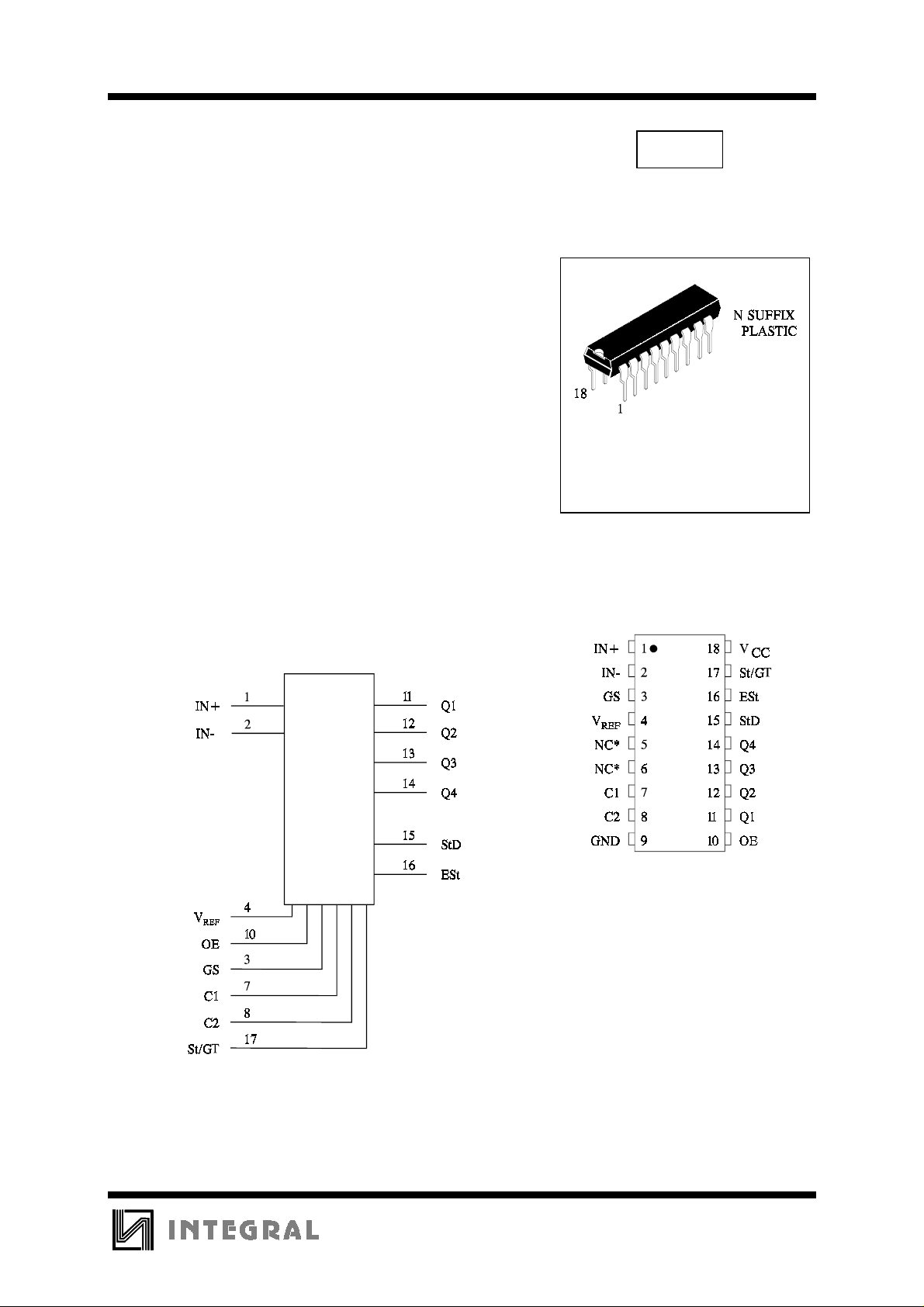
LOGIC DIAGRAM
PIN ASSIGNMENT
*
Connect to GND
PIN 9 = GND
PIN 18 = V
PINS 5,6 = NO CONNECTION
CC
1
Page 2
IN9270
PIN DESCRIPTIONS
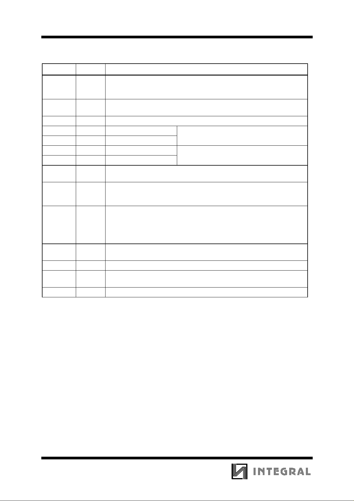
NAME PIN
ESt 16 Early steering output. Presents a logic high immediately when the digital
algorithm detects a recognizable tone-pair (signal condition). Any momentary loss
of signal condition will cause ESt to return to a logic low.
GS 3 Gain Select. Gives access to output of front-end differential amplifier for
connection of feedback resistor.
IC 5,6 Internal Connection. Must be tied to GND.
IN+ 1 Non-Inverti ng Input Connections to the front-end
IN- 2 Inverting Input
C1 7 Clock Input 3.579545 MHz crystal connected between
C2 8 Clock Output
Q1-Q4 11-14 3-state data outputs. When enabled by OE, provide the code corresponding to the
last valid tone-pair received.
StD 15 Delayed steering output. Presents a logic high when a received tone-pair has been
registered and the output latch updated; returns to logic low when the voltage on
St/GT falls below V
TSt
.
St/GT 17 Steering input/guard time output (bi-directional). A voltage greater than V
detected at St causes the device to register the detected tone-pair and update the
output latch. A voltage less than V
The GT output acts to reset the external steering time-constant; its state is a
function of ESt and the voltage on St.
OE 10 3-state output enable (input). Logic high enables the outputs Q1-Q4. Internal pull-
up.
V
CC
V
REF
18 Positive power supply, +5 V.
4 Reference voltage output, nominally VCC /2. May be used to bias the inputs at
mid-rail.
GND 9 Negative power supply, normally connected to 0 V.
DESCRIPTION
differential amplifier.
these pins completes internal oscillator.
frees the device to accept a new tone-pair.
TSt
TSt
,
FUNCTIONAL DESCRIPTION
The IN9270 monolithic DTMF receivers offer small
size, low power co nsumption and high perfor mance.
The architecture consists of a bandsplit filter section,
which separates the high and low tones of a receiver
pair, followed by a digital counting section which
verifies the frequency and duration of the received
tones before passing the corresponding code to the
output bus.
Filter Section
Separation of the low-group and high-group tones is
achieved byapplying the dual-tone signal to the inputs
2
of two filters - a sixth order for the high group and an
eight order for the low group. The band-widths of
which correspond to the bands enclosing the lowgroup and high-group tones (see Figure 1). The filter
section also incorporates notches at 350 Hz and
440 Hz for exceptional dial-tone rejection. Each filter
output is followed by a second order switchedcapacitor section which smooths the signals prior to
limiting. Limiting is performed by high-gain
comparators which are provided with hysteresis to
prevent detection of unwanted low-level signals and
noise; the outputs of the comparators provide full-rail
logic swings at the frequencies of the incoming tones.
Page 3

IN9270
Decoder Section
The decoder uses digital counting techniques to
determine the frequencies of the limited tones and to
verify that they correspond to standard DTMF
frequencies. A complex averaging algorithm protects
against tone simulation by extraneous signals, such as
voice, while providing tolerance to small frequency
deviations and variations. This averaging algorithm
has been developed to ensure an optimum
combination of immunity to “talk-off” and tolerance
to the presence of interfering signals (“third tones”)
and noise. When the detector recognizes the
simultaneous presence of two valid tones (referred to
as “signal condition” in some industry specifications),
it raises the “early steering” flag (ESt). Any
subsequent loss of signal-condition will cause Est to
fall.
Steering Circuit
Before registration of a decoded tone-pair, the
receiver checks for a valid signal duration (referred to
as “character-recognition-condition”). This check is
performed by an external RC time-constant driven by
ESt. A logic high on E St causes V
rise as the capacitor discharges. Provided signalcondition is maintained (ESt remains high) for the
validation period (t
(V
) of the steering logic to register the tone-pair,
TSt
), VC reaches the threshold
GTP
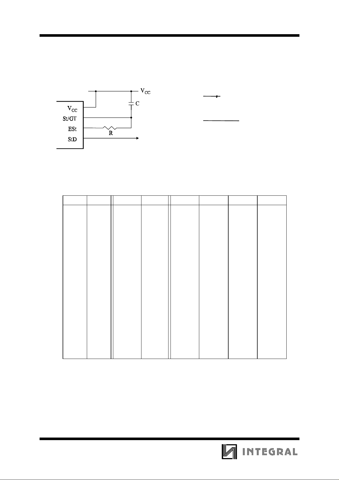
latching its corresponding 4-bit code (see Figure 3)
into the output latch. At this point, the GT output is
activated and drives V
to VCC. GT continues to drive
C
high as long as ESt remains high. Fina lly after a short
delay to allow the output latch to settle, the “delayedsteering” outp ut flag, StD, go es high, signal ing that a
received tone-pair has been registered. The contents
of the output latch are made available on the 4-bit
output bus by raising the 3-state control input (OE) to
a logic high. The st eering circuit works in re verse to
validate the interdigit pause between signals. Thus, as
well as rejecting signals too short to be considered
valid, the receiver will tolerate signal interruptions
(“drop-out”) too short to be considered a valid pause.
The facility, together with the capability of selecting
the steering time-constants externally, allows the
designer to tailor performance to meet a wide variety
of system requirements.
(see Figure 2) to
C
Guard Time Adjustment
In many situations not requiring independent
selection of receive and pause, the simple steering
circuit of Figure 2 is applicable. Component values
are chosen according to the following formula:
t
= tDP + t
REC
tID = tDA + t
The value of tDP is a parameter of the device and t
GTP
GTA
REC
is the minimum signal duration to be recognized by
the receiver. A value for C of 0.1 µF is recommended
for most applications, leaving R to be selected by the
designer. For example, a suitable value of R for a t
REC
of 40 ms would be 300 k.
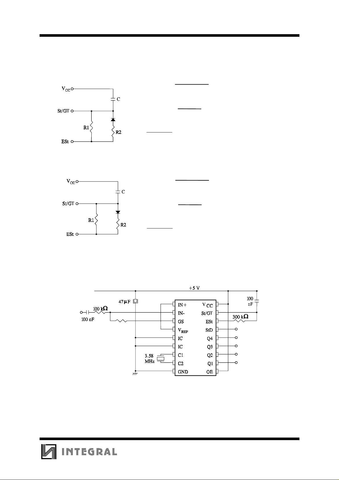
Different steering arrangements may be esed to select
independently the guard-times for tone-present (t
and tone-absent (t
). This may be necessary to meet
GTA
GTP
system specifications which place both accept and
reject limits on both tone duration and inter-digital
pause.
Guard-time adjustment also allows the designer to
tailor system parameters such as talk-off and noise
immunity. Increasing t
improves talk-off
REC
performance, since it reduces the probability that
tones simulated by speech will maintain signal
condition for long enough to be registered. On the
other hand, a relatively short t
with a long t
REC
DO
would be appropriate for extremely noisy
environments where fast acquisition time and
immunity to drop-outs would be requirements.
Design information for guard-time adjustment is
show in Figure 4.
Input Configuration
The input arrangement of the IN9270 provides a
differential-input operational amplifier as well as a
bias source (V
mid-rail.
Provision is made for connection of a feedback
resistor to the op-amp output (GS) for adjustment of
gain.
In a single-ended configuration, the input pins are
connected as shown in Figure 5 with the op-amp
connected for unity gain and V
1/2V
. Figure 6 shows the differential configuration,
CC
which permits the adjustment of gain with the
feedback resistor R
) which is used to bias the inputs at
REF
biasing the input at
REF
.
5
)
2
Page 4
IN9270
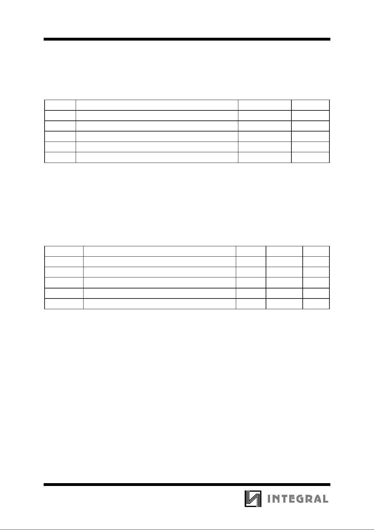
MAXIMUM RATINGS
*
Symbol Parameter Value Unit
V
CC
V
I
IN
P
DC Supply Voltage (Referenced to GND) -0.3 to +6.0 V
DC Input Voltage (Referenced to GND) -0.3 to VCC +0.3 V
IN
DC InputCurrent, per Pin 10 mA
Power Dissipation in Still Air, Plastic DIP
D
**
500 mW
Tstg Storage Temperature -65 to +150
*
Maximum Ratings are those values beyond which damage to the device may occur.
Functional operation should be restricted to the Recommended Operating Conditions.
**
Derating: -10 mW/
from 65°C to 70°C.
°
C
RECOMMENDED OPERATING CONDITIONS
Symbol Parameter Min Max Unit
V
V
T
P
tr, t
CC
IN
A
O
f
DC Supply Voltage (Referenced to GND) 4.75 5.25 V
DC Input Voltage (Referenced to GND) 1.5 3.5 V
Operating Temperature -10 +70
Power Consumption ( f = 3.579 MHz, VCC = 5 V) - 45 mW
Input Rise and Fall Time 0 110 ns
°
C
°
C
This device c ontains p rote ction ci rcuitr y to guard a gainst damage d ue to high st atic voltages or electr ic
fields. However, precautions must be taken to avoid applications of any voltage higher than maximum rated
voltages to this high-impedance circuit. For proper operation, V
GND≤(V
IN
or V
OUT
)≤VCC.
Unused inputs must always be tied to an appropriate logic voltage level (e.g., either GND or V
and V
IN
should be constrained to the range
OUT
CC
Unused outputs must be left open.
2
).
Page 5
IN9270
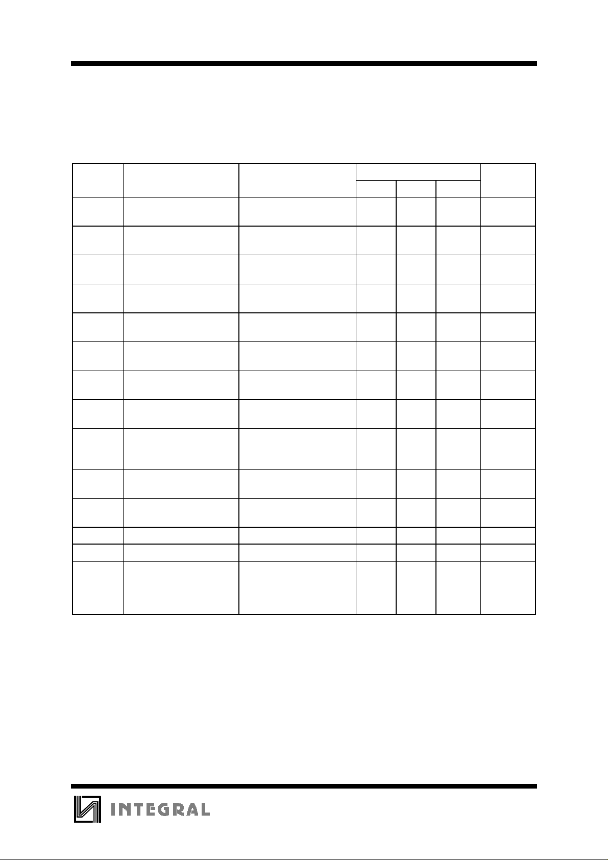
DC ELECTRICAL CHARACTERISTICS
= -10 to +70°C)
T
A
(Voltages Referenced to GND, VCC = 5 V ± 5%,
Guaranteed Limits
Symbol Parameter Test Conditions Min Typ Max Unit
V
Minimum High-Level
IH
V
=5 V 3.6 V
OUT
Input Voltage
V
Maximum Low-Level
IL
V
=5 V 1.4 V
OUT
Input Voltage
V
OH
Minimum High-Level
No Load 4.97 V
Output Voltage
V
OL
Maximum Low-Level
No Load 0.05 V
Output Voltage
I
IN
Maximum Input Leakage
VIN=VCC or GND
±
0.1
Current
I
SO
Maximum Pull Up
OE = 0 V 24
(Source) Current
I
OL
Minimum Output-L ow
V
=0.4 V 0.8 mA
OUT
(Sink) Current
I
OH
Minimum Output-High
V
=4.6 V 0.35 mA
OUT
(Source) Current
I
CC
Maximum Quiescent
V
IN =VCC
11 mA
Supply Current (per
Package)
V
TSt
Steering Threshold
2.2 2.5 V
Voltage
R
IN
Input Impedance (Signal
@ 1 KHz 8
Inputs 1,2)
V
REF
R
OR
I
OZ
Output Voltage No Load 2.4 2.8 V
Output Resistance 10
Maximum Three-State
Leakage current
Output in HighImpedance State
V
IN =VIL
V
OUT=VCC
or GND
±
0.1
M
µ
A
µ
A
Ω
Ω
k
µ
A
3
Page 6
IN9270
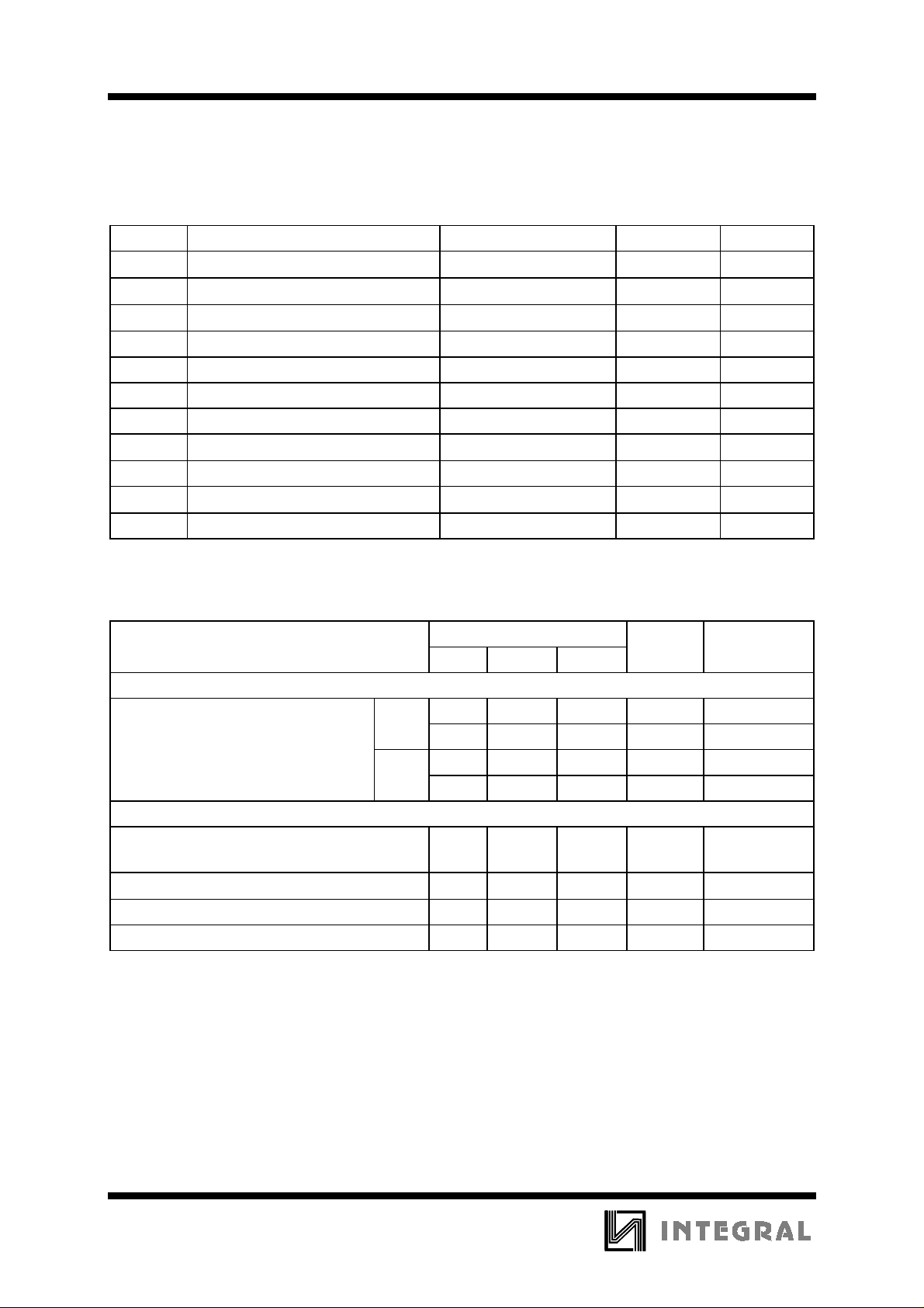
OPERATING CHARACTERISTICS
Gain Setting Amplifier
Symbol Parameter Test Conditions Typ Unit
I
N
R
IN
V
OS
PSRR Power Supply Rejection 1 KHz 60 dB
CMRR Common Mode Rejection -3.0 V < VIN < 3.0 V 60 dB
A
VOL
f
C
V
C
R
V
CM
Input Leakage Current GND< VIN < V
CC
±
100
Input Resistance 10
Input Offset Voltage
±
25
DC Open Loop Voltage Gain 65 dB
Open Loop Unity Gain Bandwidth 1.5 MHz
Output Voltage Swing
O
Tolerable Resistive Load (GS) 100 pF
L
Tolerable Resistive Load (GS) 50
L:
R
≥100 KΩ to GND
L
4.5 V
Common Mode Range No Load 3.0 V
nA
M
mV
K
Ω
PP
Ω
PP
AC ELECTRICAL CHARACTERISTICS
0 V, T
= -10 to +70°C, F
A
= 3.579545 Mhz, using test circuit of Figure 5)
CLK
(All Voltages referenced to GND. VCC = 5.0 V, GND =
Parameter Guaranteed Limits
Min Typ Max Unit Notes
SIGNAL CONDITION
Valid Input Signal MIN -29 dBm 1,2,3,5,6,9
Level (each tone of 27.5 m V
RMS
1,2,3,5,6,9
composite signal) MAX +1 dBm 1,2,3,5,6,9
883 m V
RMS
NON-ACCEPT LEVEL
Freq. Deviation Accept Limit
Freq. Deviation Reject Limit
±
3.5%
±
1.5%
±
2 Hz
Nom. 2,3,5,9
Nom. 2,3,5
Third Tone Tolerance -2.5 dB 2,3,4,5,7,9,10
Dial Tone Tolerance +18 dB 2,3,4,5,8,9,10
4
Page 7
IN9270
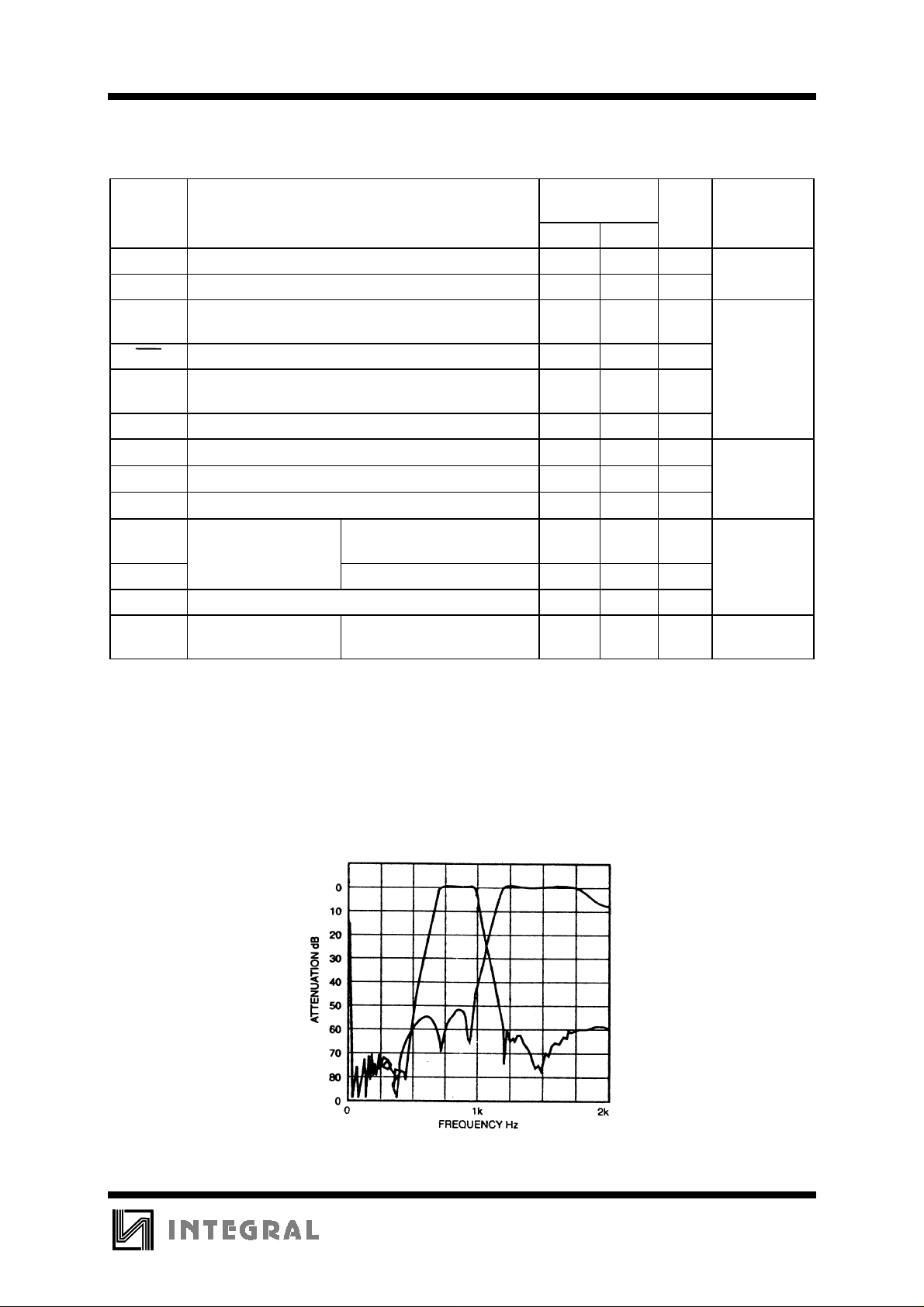
TIMING REQUIREMENTS
+70°C, F
= 3.579545 Mhz, using test circuit of Figure 5)
CLK
(All Voltages referenced to GND. VCC = 5.0 V, GND = 0 V, TA = -10 to
Symbol Parameter Guaranteed
Limits
Min Max Unit Notes
t
t
DA
t
REC
t
REC
t
t
DO
t
t
PSED
t
QSED
t
PTE
DP
ID
PQ
Tone Present Detection Time (Figure 7) 5 18 ms Refer to
Tone Absent Detection Ti me (Figure 7) 0.5 10 ms Fig. 7
Maximum Tone Detection Accept (Figure 7) 40 ms (User
Minimum Tone Detection Reject (Figure 7) 20 ms
Maximum Interdigit Pause Accept (Figure 7) 40 ms Refer to
Minimum Interdigit Pause Reject (Figure 7) 20 ms Adjustment”
Maximum Propagation Delay (St to Q) (Figure 7) 11
Maximum Propagation Delay (St to StD) (Figure 7) 16
Maximum Output Data Set Up (Q to StD) (Figure 7) 5
Maximum
ENABLE 75 ns
Propagation Delay
t
f
C
PTD
CLK
LO
(OE to Q) (Figure 7) DISABLE 460 ns
Crystal/Clock Frequency 3.5759 3.581 MHz
Clock Output (C2) Capacitive
Load
Notes:
1. dBm = decibels above or below a reference power of 1 mW into a 600 Ω load.
2. Digit sequence consists of all 16 DTMF tones.
3. Tone duration = 40 ms, Tone pause = 40 ms.
4. Nominal DTMF frequencies are used.
5. Both tones in the composite signal have an equal amlitude.
6. Tone pair is deviated by ±1.5% ±2 Hz.
7. Bandwidth limited (3 KHz) Gaussian Noise.
8. The precise dial tone frequencies are (350 Hz and 440 Hz) ±2%.
9. For an error rate of less than 1 in 10,000.
10. Referenced to the lowest level frequency component in DTMF signal.
µ
µ
µ
30 pF
s
s
s
Adjustable)
“Guard T ime
OE = V
R
C
= 10 K
L
= 50 pF
L
CC
Ω
Figure 1. Typical Filter Characteristic
5
Page 8
IN9270
t
= (RC) ln
GTA
t
= (RC) ln
GTA
Figure 2. Basic Steering Circuit
( )
( )
V
CC
V
TST
V
CC
VCC - V
TST
F
LOW
697 1209 1 H 0 0 0 1
697 1336 2 H 0 0 1 0
697 1477 3 H 0 0 1 1
770 1209 4 H 0 1 0 0
770 1336 5 H 0 1 0 1
770 1477 6 H 0 1 1 0
852 1209 7 H 0 1 1 1
852 1336 8 H 1 0 0 0
852 1477 9 H 1 0 0 1
941 1336 0 H 1 0 1 0
941 1209 * H 1 0 1 1
941 1477 # H 1 1 0 0
697 1633 A H 1 1 0 1
770 1633 B H 1 1 1 0
852 1633 C H 1 1 1 1
941 1633 D H 0 0 0 0
“L = Logic Low, H = Logic High, Z = Hi gh Impedance”
F
HIGH
KEYOEQ4Q3Q2Q1
ANYLZZZZ
Figure 3. Logic Table
6
Page 9
IN9270
t
= (RPC) ln
GTP
t
= (R
R
C) ln
1
1 R2
GTA
RP =
R
+ R
1
a) Descreasing t
= (R1C) ln
t
GTP
t
= (RPC) ln
GTA
R
1 R2
RP =
R
+ R
1
V
CC
( )
VCC - V
V
TST
CC
( )
V
TST
2
( t
GTP
V
CC
< t
GTA
GTP
( )
VCC - V
V
TST
CC
( )
V
TST
2
)
( t
> t
b) Descreasing t
GTA
GTP
GTA
)
Figure 4.Guard Time Adjustment
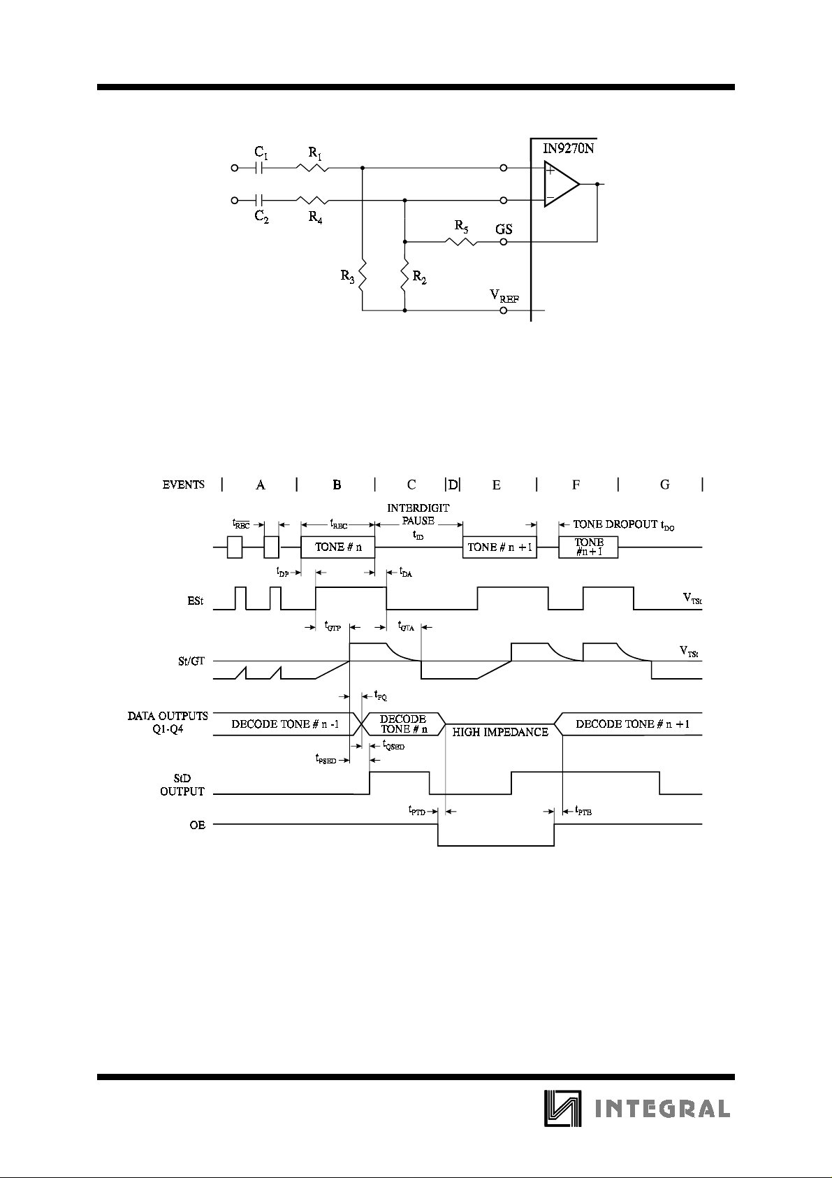
Figure 5. Single Ended Input Configuration
7
Page 10
IN9270
Figure 6. Differential Input Configuration
TIMING DIAGRAM
A. Short tone bursts: detected. Tone duration is invalid.
B. Tone #n is detected. Tone duration is valid. Decoded to outputs.
C. End of tone #n is detected and validated.
D. 3 State outputs disabled (high impedance).
E. Tone #n+1 detected. Tone duration is valid. Decoded to outputs.
F. Tristate outputs are enabled. Acceptable drop out of tone #n+1 does not register at outputs.
G. End of tone #n+1 is detected and validated.
8
Page 11
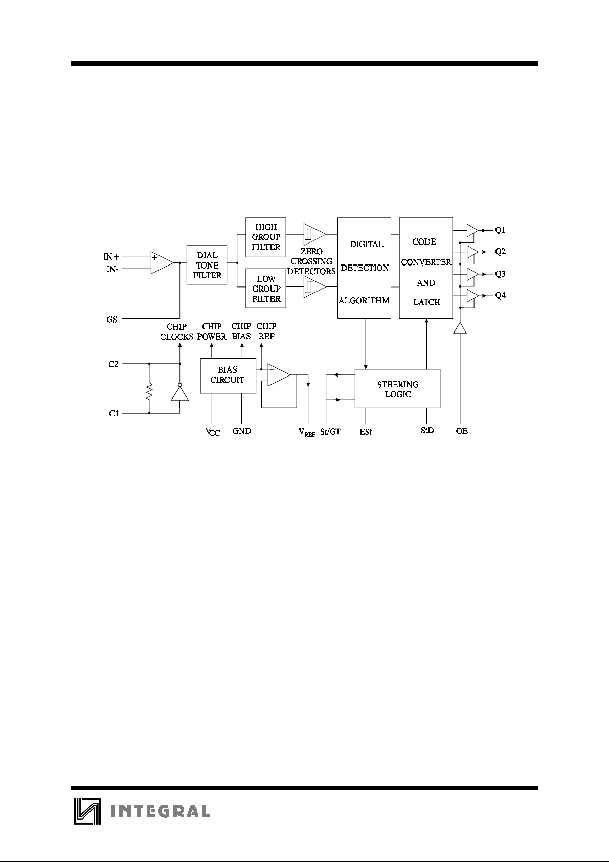
EXPANDED LOGIC DIAGRAM
IN9270
9
 Loading...