

Page 1
TECHNICAL DATA
1
PULSE DIALER
The IN9151-3 pulse dialer is a monolithic CMOS integrated circuit which
converts pushbutton inputs to a series of pulses suitable for telephone
dialing. It is intended to replace mechanical telephone dialers and can
operate directly from telephone lines. CMOS technology is used to
produced this device, resulting in very low power requirements and high
noise immunity. The IN9151-3 can be easily interfaced with a variety of
telephones, requiring only a minimal number of external components.
•
Direct telephone line operation
•
4 x 3 matrix keyboard interface
•
Supply voltage range of 2.0 to 5.5 volts
•
Inexpensive RC oscillator
•
Low power standby mode for redialing
•
22-digit redial memory
•
Redial with either * or # key
•
Dialer reset for line power breaks > 200 ms
•
Selectable make/break ratio
•
High speed test capacity
IN9151-3
ORDERING INFORMATION
IN9151N-3 Plastic
TA = -20° to 70° C for package
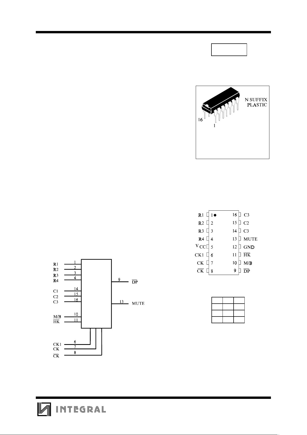
PIN ASSIGNMENT
KEYBOARD ASSIGNMENT
R1123
R2456
R3789
R4 * 0 #
C1 C2 C3
(*,# : Redial)
LOGIC DIAGRAM
PIN 5 = V
CC
PIN 12 = GND
Page 2
IN9151-3
2
PIN DESCRIPTION
PIN No. NAME
DESCRIPTION
1
2
3
4
14
15
16
R1~R4
C1~C3
Key inputs.
These inputs can be interfaced to either an XY matrix keyboard or a 2 of 7 type
keyboard. The keypad inputs are normally held at high. When a key is depressed,
scanning signals are presented at C1, C2, and C3 inputs; the dialer identifies the
key by examining the R1~R4 inputs. Debouncing is provided to avoid false entry.
5
12
V
CC
GND
Positive power supply input.
Negative power supply input.
6
7
8
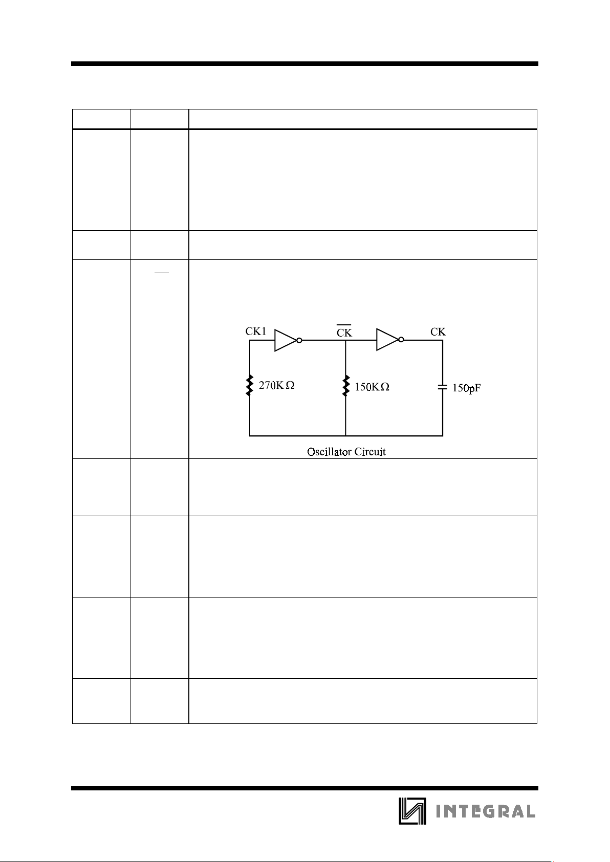
CK1,CK,
CK
Oscillator circuit input/output.
The oscillator consists of two inverters, with oscillator frequency controlled by
external RC components:
R
CK1
=270KΩ, RCK=150KΩ, CCK=150 pF
9__
DP
Dialing pulse output.
This output consists of an N-channel open drain device. Normally this output will
be in off state during make and on during break. Dialing pulse rate = 10pps and
inter-digital pause = 800 ms when F
OSC
=18KHz in normal mode.
10 M/B Make/Break ratio select input.
In normal mode, this input is used to select the Make/Break ratio:
when input = V
CC
, M/B ratio = 1/2.
when input = GND, M/B ratio = 2/3.
when connected to the clock output (pin 7), this input can trigger the IN9151-3
into test mode, generating high speed dialing.
11 __
HK
Hook switch input.
This input is used to detect whether the telephone is in the On-Hook or Off-Hook
state:
V
CC
=on-hook
GND=off-hook.
(Resetting time = 200 ms minimum)
13 MUTE Mute output.
This output is an inverter normally at low state when there is no key entry. During
outdialing it changes to high state and is used to mute the speech network.
Page 3
IN9151N-3
3
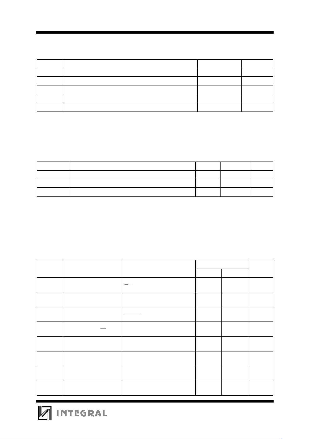
MAXIMUM RATINGS
*
Symbol Parameter Value Unit
V
CC
DC Supply Voltage (Referenced to GND) -0.3 to +5.5 V
V
IN
DC Input Voltage (Referenced to GND) -0.3 to VCC +0.3 V
P
D
Power Dissipation in Still Air , Plastic DIP
**
600 mW
Tstg Storage Temperature -55 to +150
°
C
T
L
Lead Temperature, 1mm from case for 10 seconds 260
°
C
*
Maximum Ratings are those values beyond which damage to the device may occur.
Functional operation should be restricted to the Recommended Operating Conditions.
**
Durating: -10 mW/
°
C
from 65°C to 70°C.
RECOMMENDED OPERATING CONDITIONS
Symbol Parameter Min Max Unit
V
CC
DC Supply Voltage (Referenced to GND) 2.0 5.5 V
V
IN
DC Input Voltage (Referenced to GND) 0 V
CC
V
T
A
Operating Temperature -10 +70
°
C
This device contains protection circuitry to guard against damage due to high static voltages or electric
fields. However, precautions must be taken to avoid applications of any voltage higher than maximum rated
voltages to this high-impedance circuit. For proper operation, V
IN
and V
OUT
should be constrained to the range
GND≤(V
IN
or V
OUT
)≤VCC.
Unused inputs must always be tied to an appropriate logic voltage level (e.g., either GND or V
CC
).
Unused outputs must be left open.
DC ELECTRICAL CHARACTERISTICS
(Voltages Referenced to GND, VCC = 2.0 V to5.5 V,
T
A
= -20 to +70°C)
Guaranteed Limits
Symbol Parameter Test Conditions Min Max Unit
I
MR
Maximum Memory
Retention Current
VCC=1.0 V,
HK=VCC ,all outputs unloaded
1
µ
A
I
CC
Maximum Supply
Operating Current
oscillator running, all outputs
unloaded
200
µ
A
I
SB
Maximum Standby
Current
all outputs unload
HK=V
CC
4
µ
A
I
OL
Minimum Output Sink
Current (Mute, DP)
V
CC
=2.0V, V
OUT
=0.5V,
f=18KHz
2mA
I
OH
Minimum Output Drive
Current (Mute)
VCC=2.0V,
V
OUT=VCC
-1V, f=18KHz
1mA
V
IL
Min High-Level Input
Voltage
0.8V
CC
V
CC
V
CC
V
IL
Max Low-Level Input
Voltage
GND 0.2V
CC
I
IN
Max. Input Leakage
Current
VCC=5.5V
±
1.0
µ
A
Page 4
IN9151-3
4
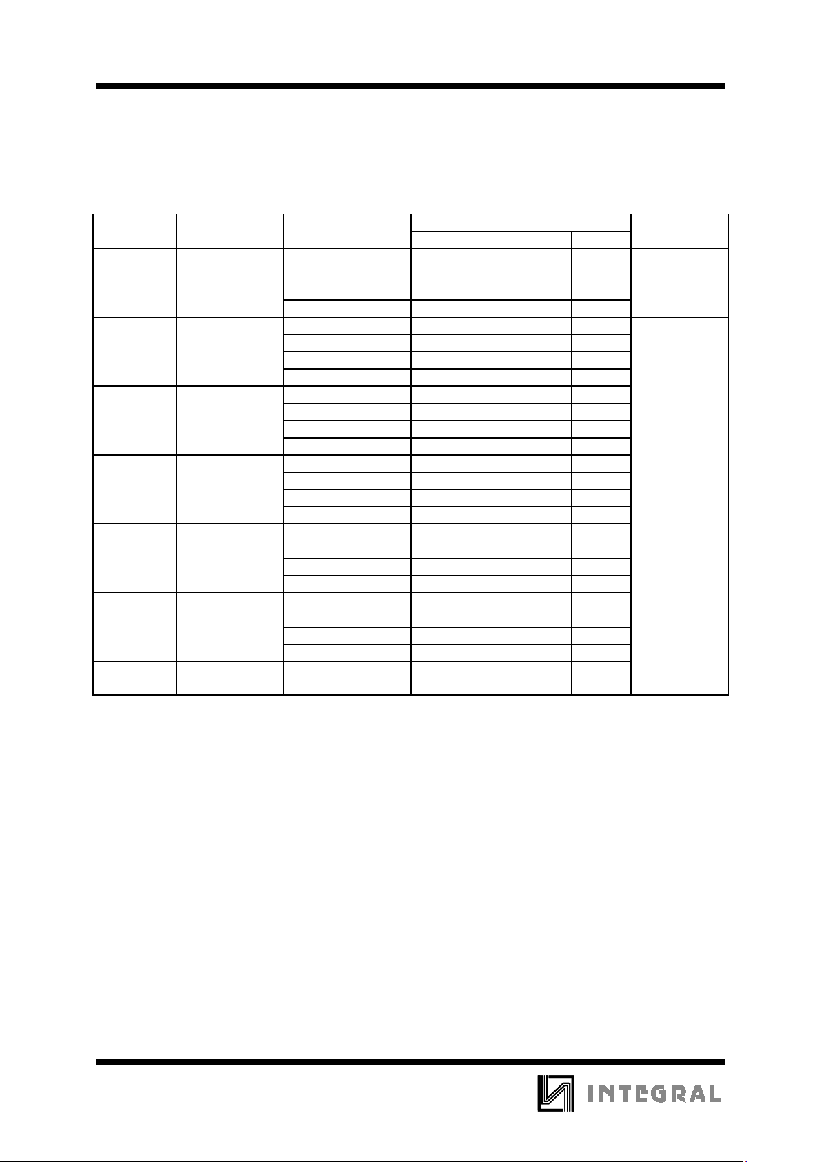
AC ELECTRICAL CHARACTERISTICS
(F
OSC
= 18 KHz, VCC=2.0 to 5.5 V, TA=-20
to +70°C )
Symbol Parameter Test Conditions Guaranteed Limit Unit
Min. Typ. Max
M/B Make/Break M/B=V
CC
1/2
Ratio M/B=GND 2/3
DR Dial Pulse F
OSC
=18KHz 10 pps
Rate F
OSC
=36KHz 20
Maximum 10pps 1/2 33
T
M
Make Time 10pps 2/3 40 ms
(Figure 3) 20pps 1/2 16.6
20pps 2/3 20
Maximum 10pps 1/2 66
T
B
Break Time 10pps 2/3 60
(Figure 3) 20pps 1/2 33
20pps 2/3 30
Maximum 10pps 1/2 800
T
IDP
Inter-digital 10pps 2/3 800
Pause Time 20pps 1/2 400
(Figure 3) 20pps 2/3 400
Maximum 10pps 1/2 800
T
PDP
Pre-digital 10pps 2/3 800
Pause 20pps 1/2 400
(Figure 3) 20pps 2/3 400
Maximum 10pps 1/2 33
T
MDP
Mute Delay 10pps 2/3 40
Time 20pps 1/2 16.6
(Figure 3) 20pps 2/3 20
T
KD
Minimum Key
Debounce Time
VIN=GND
or V
CC
30
Page 5
IN9151N-3
5
Operation Procedures
Symbol Definitions:
D
P
: pulse digit (0 through 9)
ZiZiZi: conversation
0-0↑: off-hook.
0-0↓: on-hook.
* or # : Redial
Recommended Operations:
Normal Dialing:
0-0↑; D
P
... DP; ZiZiZi; 0-0
↓
Dial pulse begins as soon as first key is entered.
Debounced and detected on chip.
Redialing:
0-0↑; * or # key
(* or # key can be accepted as first key entry after
Off-Hook.)
Functional Description
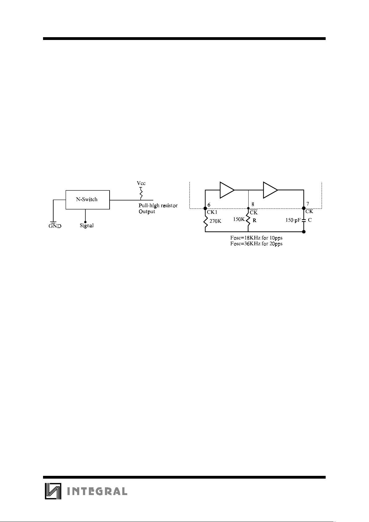
1) N-channel open drain output - DP (Figure 1).
2) Clock oscillator
The clock oscillator consists of two inverters, with
the frequency of oscillation controlled by external
components connected to pins 6,7, and 8. The
circuit is sufficiently versatile to allow the use of a
variety of external component configurations. The
oscillator circuit is shown in figure 2.
Figure 1
Figure 2
Page 6
IN9151-3
2
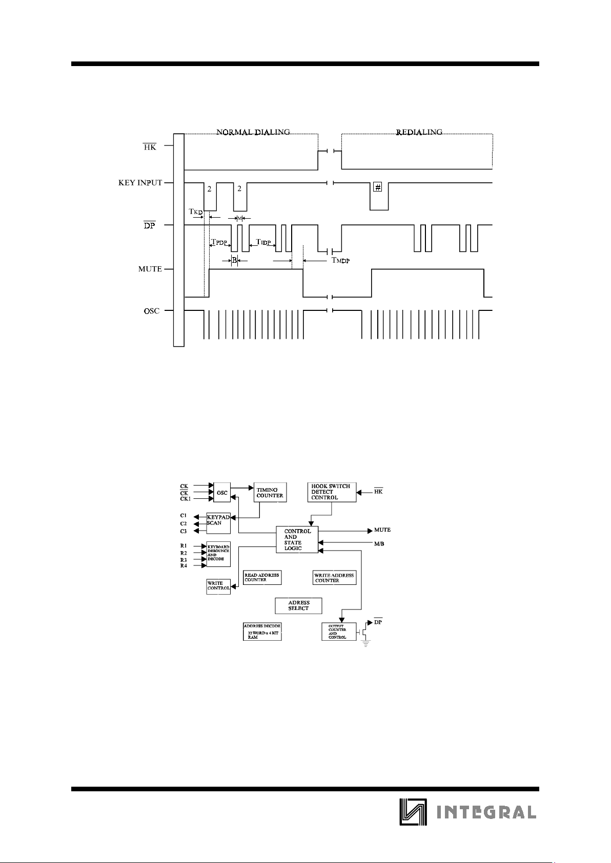
SWITCHING WAVEFORMS
EXPANDED LOGIC DIAGRAM
 Loading...