

Page 1

TECHNICAL DATA
1
10 Memory Tone/Pulse Dialer
High-Performance Silicon-Gate CMOS
The IN91260C is tone/pulse switchable dialer with ten 16-digit
number memories and 32-digit redial memory. Pulse to tone mode
switching is performed via a slide switch.
•
32-digit redial memory (31 digits in tone mode)
•
Ten indirect memories, 16 digits in pulse mode, 15 digits in tone
mode
•
Tone/Pulse mode switching via slide switch (4.1 second pause
inserted automatically)
•
Wide operating voltage: 1.8 V ∼ 5.5 V
•
Uses 480 KHz ceramic resonator
•
Low memory retention current
•
Selectable Make/Break ratio
•
Dial Pulse Rate: 10 pps
Keyboard Assignments*
123 S R1
456 A/L R2
789 P R3
*0# R R4
C1 C2 C3 C4
IN91260C
ORDERING INFORMATION
IN91260CN
TA = -20° to 70° C
PIN ASSIGNMENT
LOGIC DIAGRAM
PIN 11 = GND
PIN 10 = V
CC
S: Store
A/L : Auto/Location
P: Pause
R: Redial
Page 2
IN91260C
2
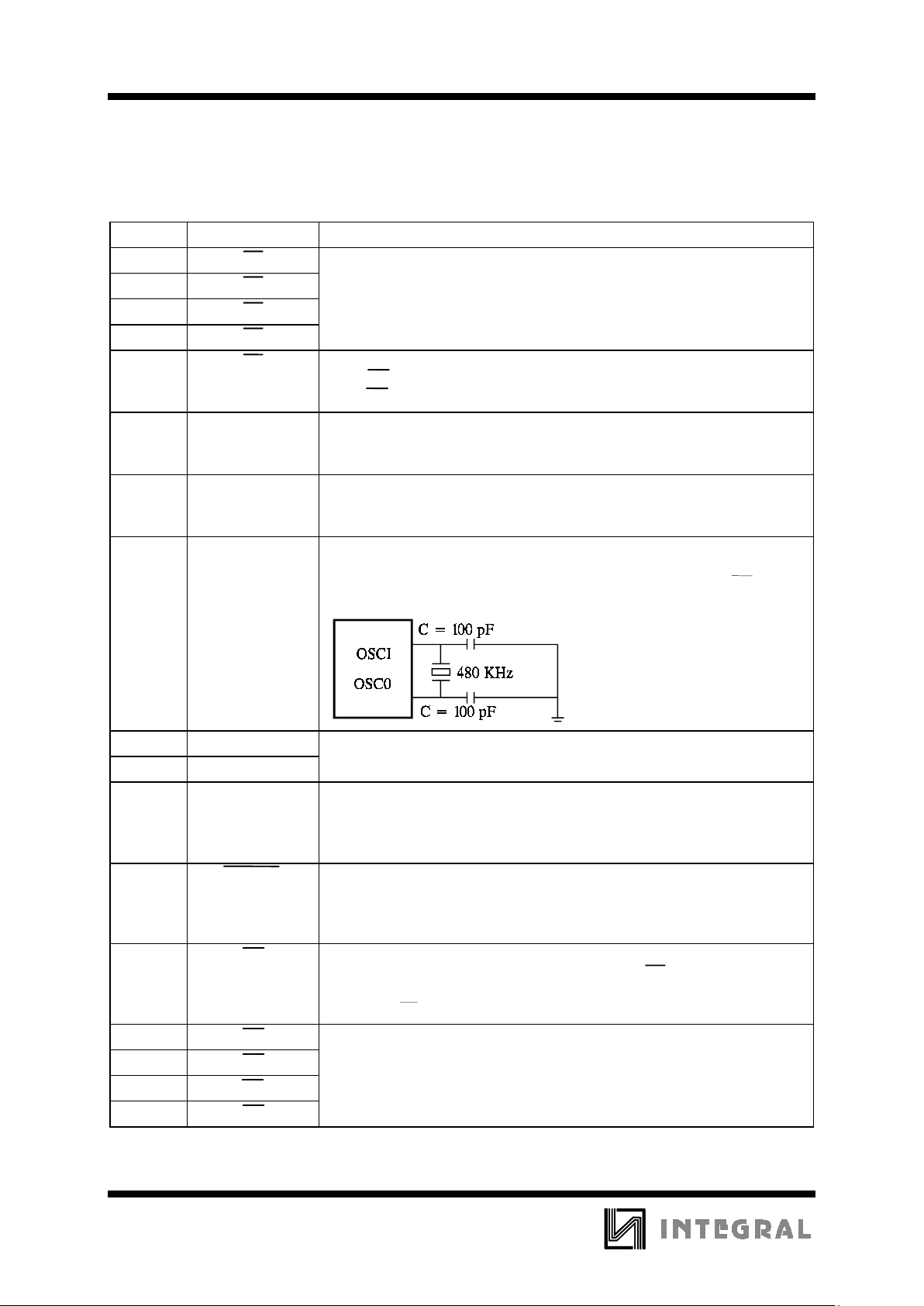
Pin Description
Pin No. Designation Description
1R1
2R2
3R3
4R4
5 HK Hook switch input.
When HK = V
CC
, an ON-Hook state exists.
When HK = GND, an Off-Hook state exists.
6 M/B Dial pulse Make/Break ratio select input.
If M/B = V
CC
, the Make/Break ratio is 1/2.
If M/B = GND, the Make/Break ratio is 2/3.
7 MODE SELECT Pulse/DTMF mode select input.
If MODE SELECT = V
CC
, Pulse mode is in effect.
If MODE SELECT = GND, DTMF mode is in effect.
8
9
OSCI
OSC0
Oscillator I/O.
A 480 KHz ceramic resonator and two 100 pF serial loading capacitors form
a complete oscillator circuit. The circuit is activated when HK is low.
Oscillator start-up time is typically 10 ms.
10 V
CC
11 GND
12 TONE DTMF signal output.
Pull-down load resistance is 10,000 Ω.
The minimum tone and IDP durations are built-in for both normal dialing
and redialing.
13 XMUTE Transmit mute output.
This is an N-channel open drain output. The output transistor is switched on
while a sequence of digits is being dialed (for both Pulse and Tone modes).
Otherwise, it is switched off.
14 DP Dial pulse output.
This pin is an N-channel open drain output. When DP output is low
(switched on), it serves as a break signal in Pulse dialing. For other
operations, DP output is normally high impedance (switched off).
15 C1
16 C2
17 C3
18 C4
Keyinputs.
When a row and a column are connected, a key operation is activated.
Scanning signals are present on both the row and column pins during a
valid key-in condition.
Keyinputs.
When a row and a column are connected, a key operation is activated.
Scanning signals are present on both the row and column pins during a valid
key-in condition.
Positive power supply.
Negative power supply.
Page 3
IN91260C
3
Operation Procedures
Symbol Definitions:
a. D
P
: Pulse digit, 1, 2, 3, 4, 5, 6, 7, 8, 9, 0
b. D
t
: tone digit, 1, 2, 3, 4, 5, 6, 7, 8, 9, 0, *, #
c. LOCi : i = 1, 2, 3, 4, 5, 6, 7, 8, 9, 0
d. ZiZiZi : Conversation mode
e. 0 - 0 ↑ : OFF-HOOK
f. 0 - 0 ↓ : ON-HOOK
g. : Input Level from Low to High
h. : Input Level from High to Low
Recommended dialing, redialing, mixed dialing
and storing operations:
1. Normal dialing in pulse mode
0 - 0 ↑ , D
P
. . . DP, ZiZiZi 0 - 0
↓
2. Normal dialing in tone mode
0 - 0 ↑ , D
t
. . . Dt, ZiZiZi 0 - 0
↓
3. Mixed dialing in pulse-to-tone mode
0 - 0 ↑ , D
P
. . . DP, MODE SELECT
, D
t
. . . Dt, ZiZiZi 0 - 0
↓
4. Redialing
0 - 0 ↑ , D
P
. . . D
P
0 - 0 ↓, 0 - 0 ↑, R, ZiZiZi, 0
- 0
↓
0 - 0 ↑ , D
t
. . . Dt 0 - 0 ↓, 0 - 0 ↑, R, ZiZiZi, 0
- 0
↓
5. Storing Numbers to Repertory Memory
(i) Off-hook Store 0 - 0 ↑, S , D
P
. . . D
P
or Dt . . . Dt , A/L , LOCi, 0 - 0
↓
(ii) On/Off-hook store: 0 - 0 ↓, S , D
P
. . . D
P
or
D
t
. . . Dt , A/L , LOCi
6. Dialing from Repertory Memory
0 - 0 ↑, A/L , LOCi, ZiZiZi 0 - 0
↓
Functional Description
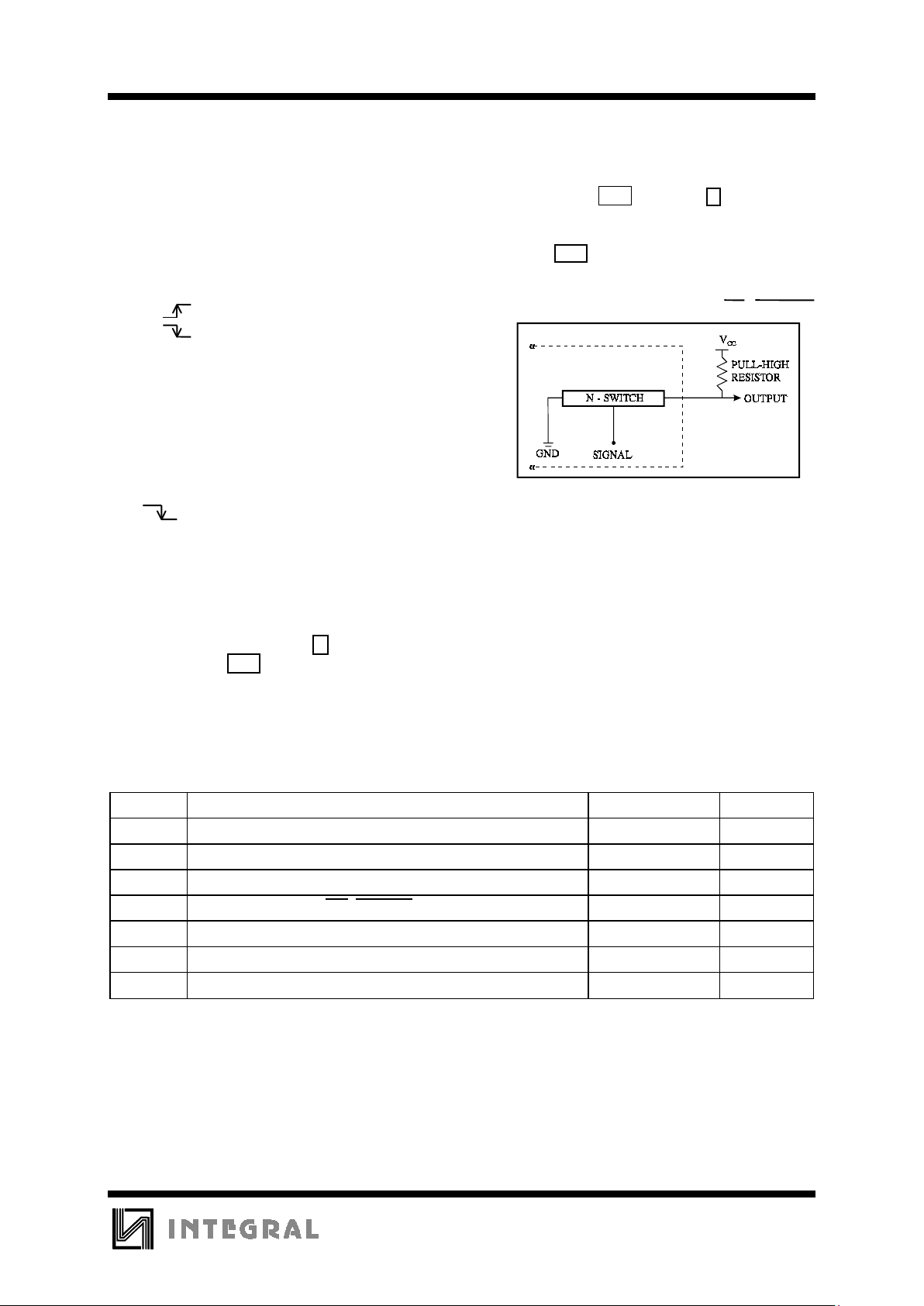
1. N-Channel Open Drain Output - DP, XMUTE
F
igure 1.
2. DTMF Generator
The digitally synthesized sinewave of the
IN91260 series is well designed, with a 6 level,
12 segment, 1/2 V
CC
reference voltage. The THD
(Total Harmonic Distortion) of the DTMF output
is typically 1%, when V
CC
= 2.5 V to 5.5 V and
frequency is in the 500 HZ to 3400 HZ band.
MAXIMUM RATINGS
*
Symbol Parameter Value Unit
V
CC
DC Supply Voltage (Referenced to GND) -0.3 to +6.0 V
V
IN
DC Input Voltage (Referenced to GND) -0.3 to VCC +0.3 V
V
OUT
DC Output Voltage (Referenced to GND) -0.3 to VCC +0.3 V
V
OUT
DC Output Voltage (DP, XMUTE) -0.3 to 1.2 V
I
TONE
DC Output Current(Tone) 50 mA
P
D
Power Dissipation in Still Air, Plastic DIP
**
500 mW
Tstg Storage Temperature -40 to +125
°
C
*
Maximum Ratings are those values beyond which damage to the device may occur.
Functional operation should be restricted to the Recommended Operating Conditions.
**
Durating: -10 mW/
°
C
from 65°C to 70°C.
Page 4
IN91260C
2
RECOMMENDED OPERATING CONDITIONS
Symbol Parameter Min Max Unit
V
CC
DC Supply Voltage (Referenced to GND) 1.8 5.5 V
V
IN
DC Input Voltage (Referenced to GND) 0 V
CC
V
V
OUT
DC Output Voltage (Referenced to GND) 0 V
CC
V
T
A
Operating Temperature -20 +70
°
C
This device contains protection circuitry to guard against damage due to high static voltages or electric
fields. However, precautions must be taken to avoid applications of any voltage higher than maximum rated
voltages to this high-impedance circuit. For proper operation, V
IN
and V
OUT
should be constrained to the range
GND≤(V
IN
or V
OUT
)≤VCC.
Unused inputs must always be tied to an appropriate logic voltage level (e.g., either GND or V
CC
).
Unused outputs must be left open.
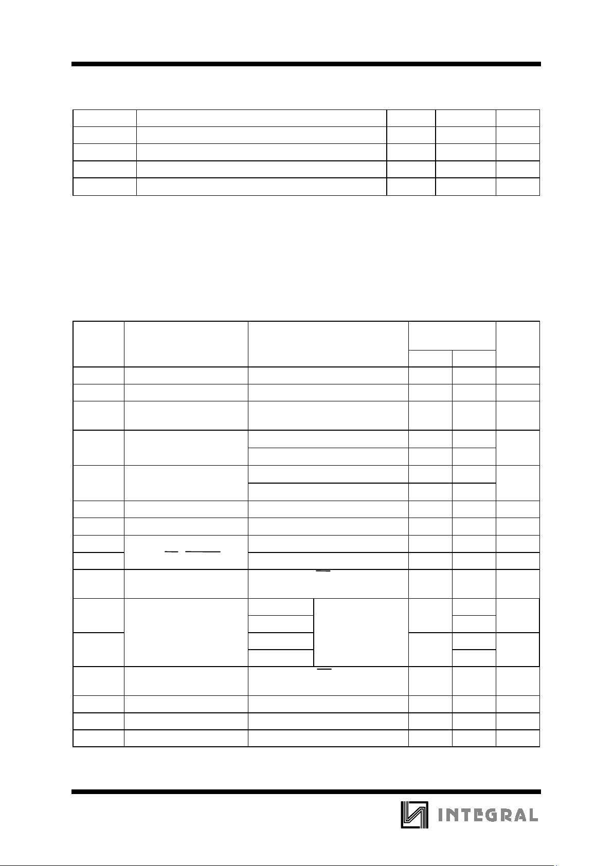
DC ELECTRICAL CHARACTERISTICS
(Voltages Referenced to GND, VCC =1.8 V to 5.5 V,
T
A
= -20 to +70°C)
Guaranteed
Limits
Symbol Parameter Test Conditions Min Max Unit
V
IH
High-Level Input Voltage 0.8V
CC
V
CC
V
V
IL
Low-Level Input Voltage 0 0.2V
CC
V
V
MR
Minimum Memory
Retention Voltage
V
CC
= 1.0 V 1.5 V
R
LOAD
= 10 KΩ VCC = 2.5 V
540 640
R
LOAD
= 10 KΩ VCC = 5.5 V
100 1300
R
LOAD
= 10 KΩ VCC = 2.5 V
410 490
R
LOAD
= 10 KΩ VCC = 5.5 V
850 990
IC * Column Input Current VIN =3.5 V All outputs unloaded 0.6 2.0 mA
IR* Row Input Current V
IN
= 0 V All outputs unloaded 5 50
µ
A
I
OL1
VCC = 3.5 V, VOL = 0.4 V 0.7 mA
I
OL2
VCC = 2.0 V, VOL = 0.4 V 0.2 mA
I
MR
Maximum Memory
Retention Current
VCC = 1.0 V, HK = V
CC
All outputs unloaded
0.6
µ
A
VCC=3.5 V 0.7
VCC=5.5 V 2.1
VCC=3.5 V 1.3
VCC=5.5 V 3.9
I
SD
Maximum Standby Current VCC = 2.5 V, HK = GND
All outputs unloaded
7.0
µ
A
T
WIST
Pre.-emphasis VCC = 3.5 V 1 3 dB
V
V
Valley of Single Tone VCC = 3.5 V 0.3 6.0 V
DD
DIS% Distortion *Note 1, V
CC
= 3.5 V 6.0 %
* @ 25 °C
Single Column Tone
Output Amplitude
Single Row Tone
Output Amplitude
Maximum Supply
Operation Current
mVp-p
mVp-p
V
OC
*
V
OR
*
Minimum Sink Output
Current DP, XMUTE
Oscillator running;
all outputs unloaded,
V
IL
= 0, VIH = V
CC
I
CCP
I
CCT
mA
mA
Page 5
IN91260C
3
Note 1:
DIS% =
a. V
1
. . . Vn are the intermodulation or the harmonic frequencies in the 500 Hz to 3400 Hz band.
b. V
OC
and VOR are the individual frequency components of the DTMF signal.
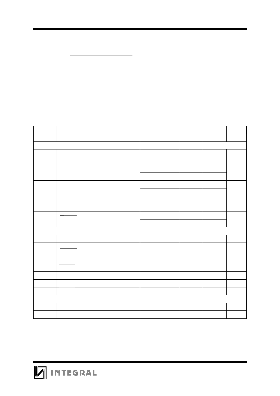
AC ELECTRICAL CHARACTERISTICS
(All Voltages referenced to GND. VCC = 1.8 V to 5.5 V,
T
A
= -20 to +70°C, F
OSK
= 480 KHz)
Guaranteed Limits
Symbol Parameter Test Conditions Min Max Unit
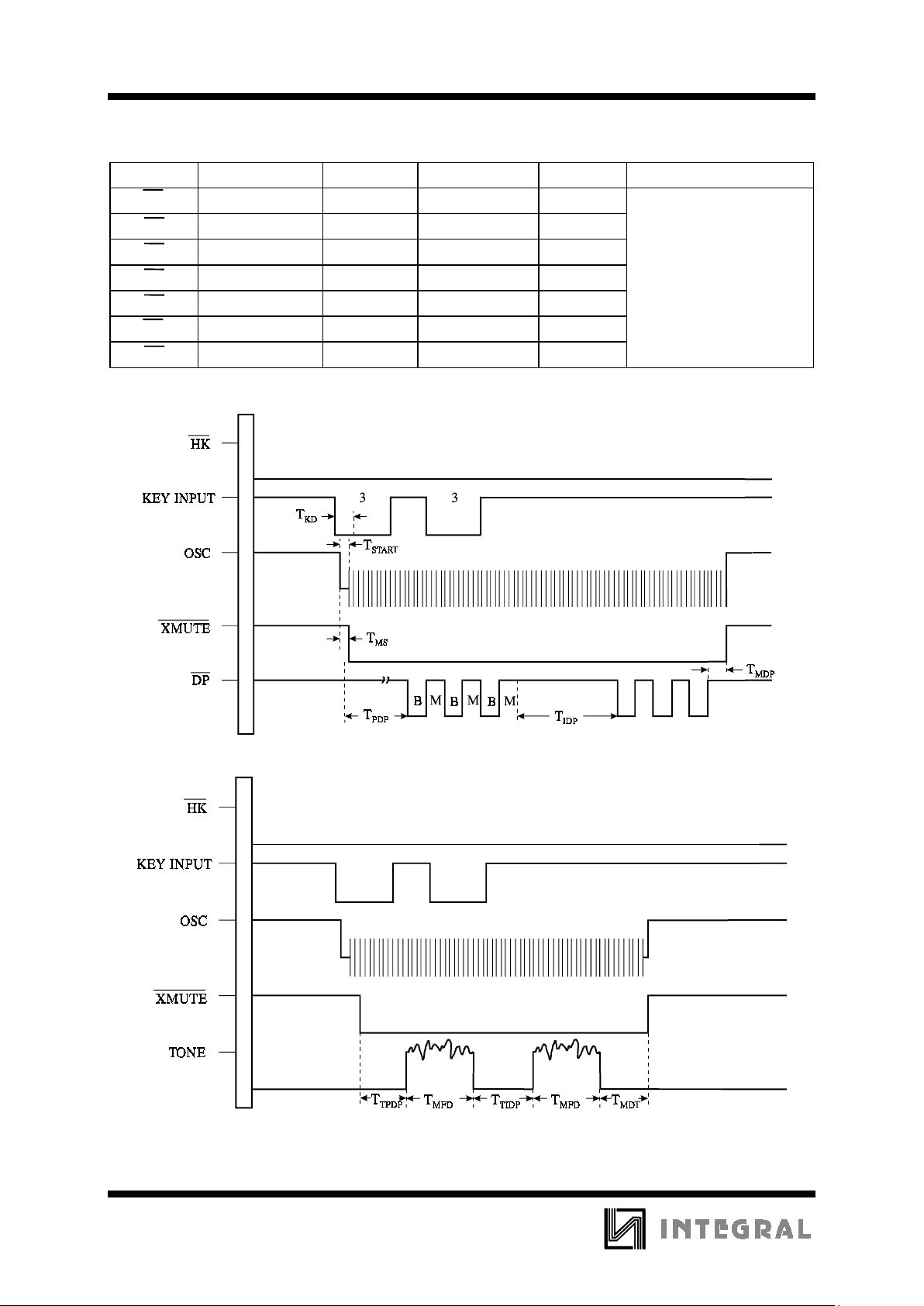
PULSE
M/B = 1/2 30 35
M/B = 2/3 38 42
M/B = 1/2 64 69
M/B = 2/3 57 63
M/B = 1/2 790 815
M/B = 2/3 790 815
M/B = 1/2 820 860
M/B = 2/3 820 860
M/B = 1/2 0 3
M/B = 2/3 0 3
TONE
T
MFD
Minimum Tone Duration (Figure 3) 100 120 ms
T
TIDP
Minimum Tone Inter-Digit Pause
(XMUTE) (Figure 3)
100 120 ms
T
TPDP
Tone Output Pre-Digit Pause (Figure 3) 115 145 ms
T
MDT
XMUTE Delay Time (Figure 3) 100 120 ms
T
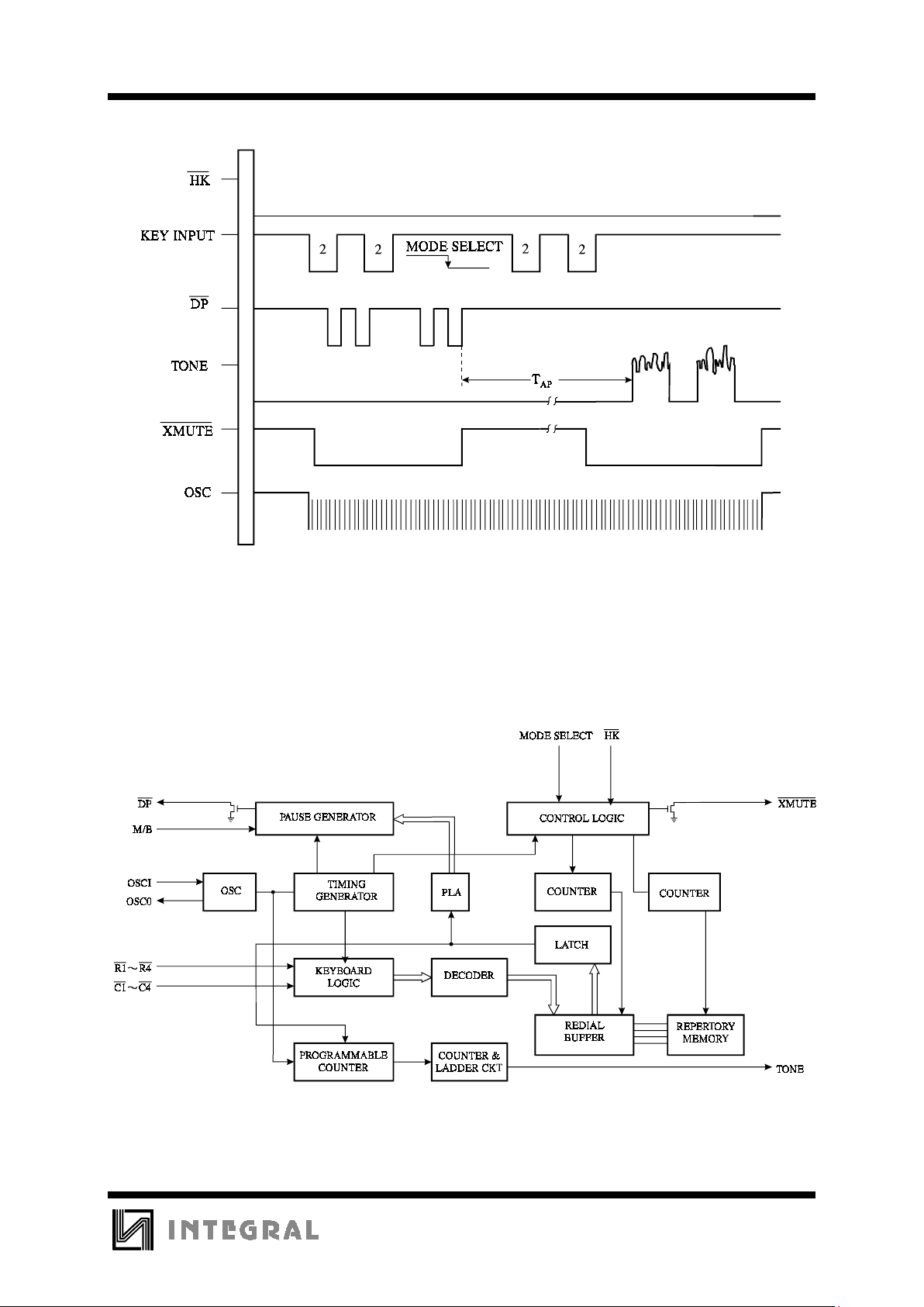
AP
Auto Pause Time (Figure 4) 3.9 4.3 s
T
START
Oscillator Start-up Time (Figure 2) 4 13 ms
T
MS
XMUTE Start-up Time (Figure 2) 25 35 ms
KEY-IN
T
KD
Keypad Debounce Time (Figure 2) 19 25 ms
F
KS
Key Scan Frequency
C1 ∼ C4, R1∼ R4
365 390 Hz
T
M
T
B
T
IDP
T
PDP
T
MDP
Make Time (Figure 2)
Break Time (Figure 2)
Inter Digit Pause Time (Figure 2)
Pre-Digit Pause (Figure 2)
XMUTE, Delay Time (Figure 2)
ms
ms
ms
ms
ms
100.(V
1
2
+ V
2
2
+. . . + V
n
2
)
1
/
2
(V
OC
2
+ V
OR
2
)
1
/
2
Page 6
IN91260C
4
Comparisons of Specified vs. Actual Tone Frequencies
R/C Spec. Actual Error(%) Unit Conditions
R1 697 695.65 -0.19 Hz
R2 770 769.23 -0.1 Hz
R3 852 851.06 -0.11 Hz
R4 941 941.18 +0.02 Hz F
OSC
=480 KHz
C1 1,209 1,212.12 +0.26 Hz
C2 1,336 1,333.33 -0.2 Hz
C3 1,477 1,481.48 +0.3 Hz
Figure 2. Pulse Mode
Figure 3. Tone Mode
Page 7
IN91260C
5
Figure 4. Normal Pulse to Tone mixed dialing via slide switch
EXPANDED LOGIC DIAGRAM
 Loading...