

Page 1
TECHNICAL DATA
1
Octal 3-State Noninverting Buffer/Line
Driver/Line Receiver
These octal buffers and line drivers and designed specifically to
improve both the performance and density of three-state memory
address drivers, clock drivers, and busoriented receivers and
transmitters.
This devise features high fan-out, improved fan-in, and 400 mV
noise margin.
It can be used to drive terminated lines down to 133 ohms.
•
3-State Outputs Drive Bus Lines or Buffer Memory Address
Registers
•
P-N-P Inputs Reduce D-C Loading
•
Hysteresis at Inputs Improves Noise Margins
IN74LS244
ORDERING INFORMATION
IN74LS244N Plastic
IN74LS244DW SOIC
TA = 0° to 70° C
for all packages
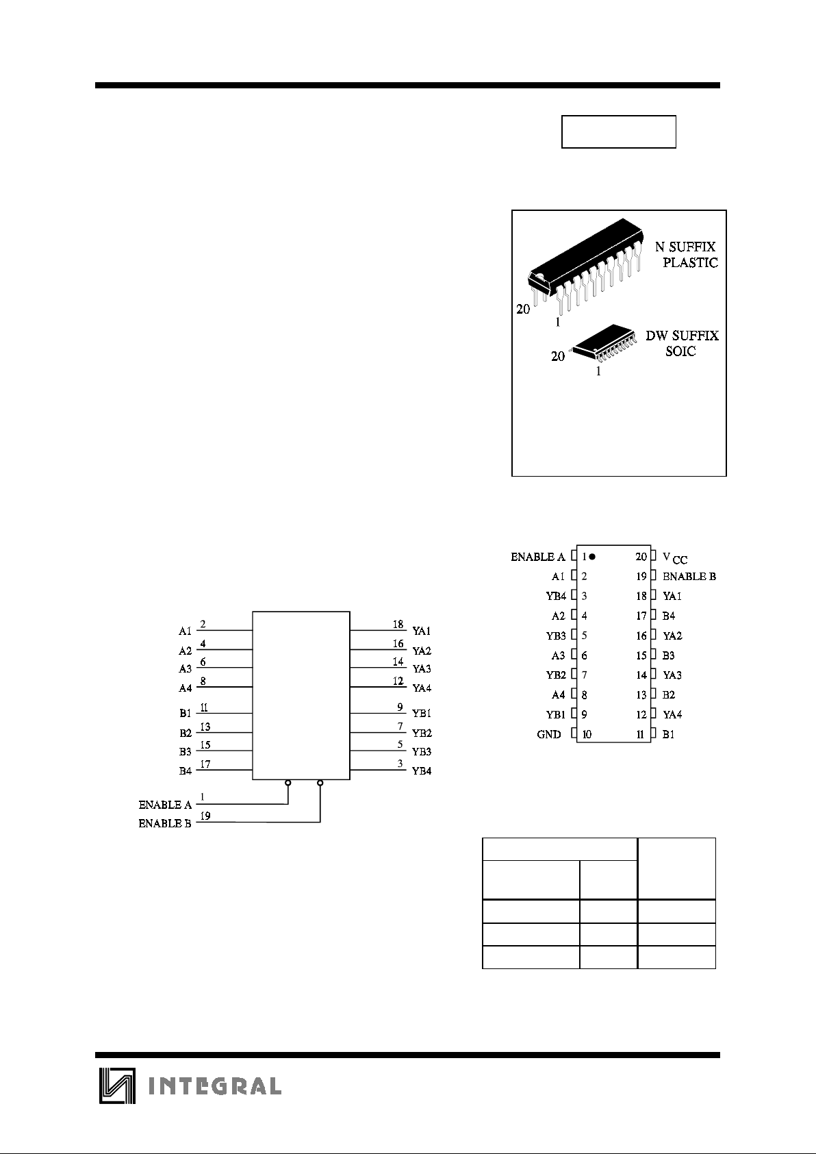
FUNCTION TABLE
Inputs Outputs
Enable A,
Enable B
A,B YA,YB
LLL
LHH
HXZ
X=don’t care
Z = high impedance
LOGIC DIAGRAM
PIN 20=V
CC
PIN 10 = GND
PIN ASSIGNMENT
Page 2
IN74LS244
2
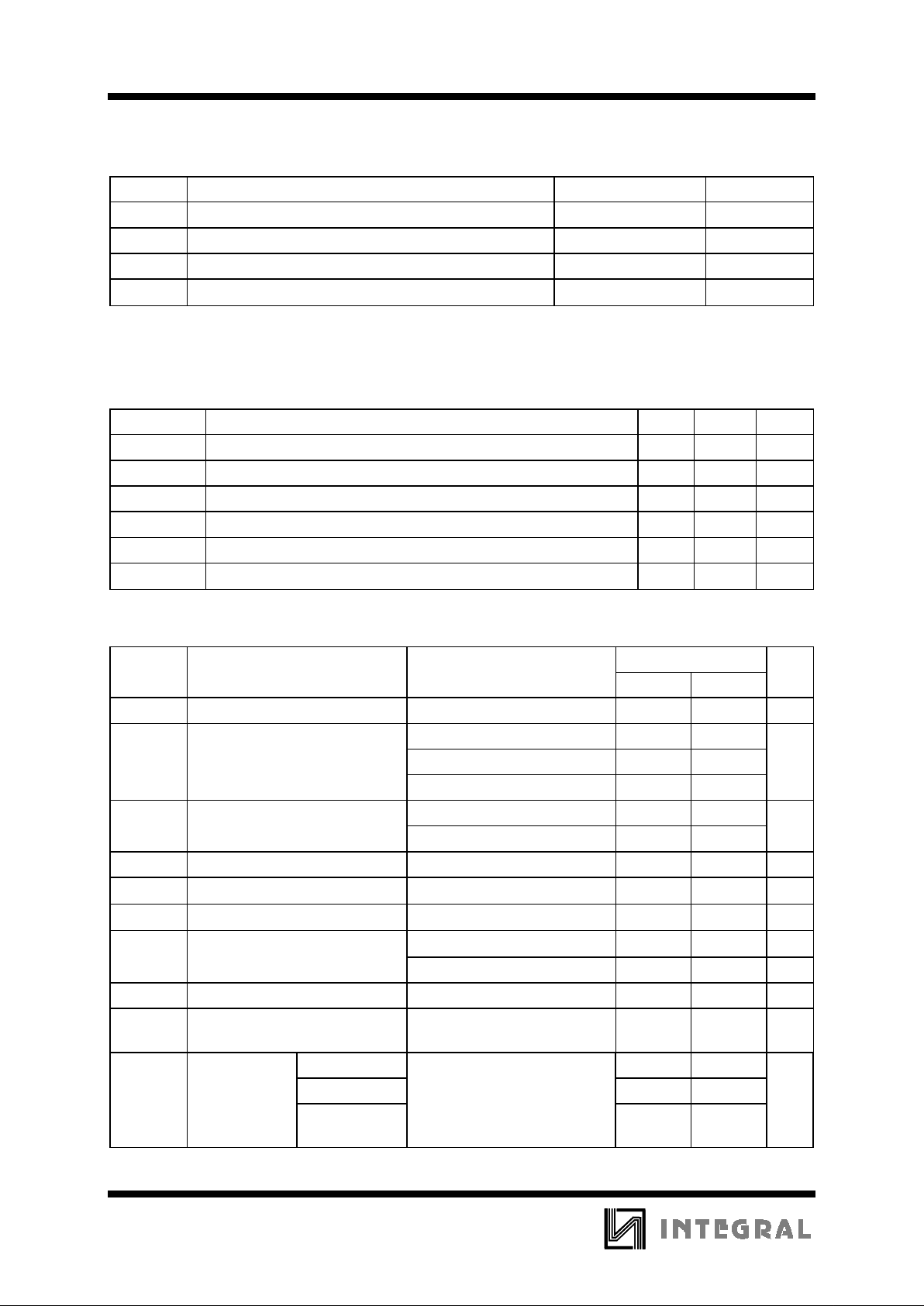
MAXIMUM RATINGS
*
Symbol Parameter Value Unit
V
CC
Supply Voltage 7.0 V
V
IN
Input Voltage 7.0 V
V
OUT
Output Voltage 5.5 V
Tstg Storage Temperature Range -65 to +150
°
C
*
Maximum Ratings are those values beyond which damage to the device may occur.
Functional operation should be restricted to the Recommended Operating Conditions.
RECOMMENDED OPERATING CONDITIONS
Symbol Parameter Min Max Unit
V
CC
Supply Voltage 4.75 5.25 V
V
IH
High Level Input Voltage 2.0 V
V
IL
Low Level Input Voltage 0.8 V
I
OH
High Level Output Current -15 mA
I
OL
Low Level Output Current 24 mA
T
A
Ambient Temperature Range 0 +70
°
C
DC ELECTRICAL CHARACTERISTICS
over full operating conditions
Guaranteed Limit
Symbol Parameter Test Conditions Min Max Unit
V
IK
Input Clamp Voltage VCC = min, IIN = -18 mA -1.5 V
V
OH
High Level Output Voltage VCC = min, IOH = -1.0 mA 2.7 V
VCC = min, IOH = -3.0 mA 2.4
VCC = min, IOH = -15 mA 2.0
V
OL
Low Level Output Voltage VCC = min, IOL = 12 mA 0.4 V
VCC = min, IOL = 24 mA 0.5
VT+ - VT-Hysteresis VCC = min 0.2 V
I
OZH
Output Off Current HIGH VCC = max, V
OUT
= 2.7 V 20
µ
A
I
OZL
Output Off Current LOW VCC = max, V
OUT
= 0.4 V -20
µ
A
I
IH
High Level Input Current VCC = max, VIN = 2.7 V 20
µ
A
VCC = max, VIN = 7.0 V 0.1 mA
I
IL
Low Level Input Current VCC = max, VIN = 0.4 V -0.2 mA
I
O
Output Short Circuit Current VCC = max, VO =0 V
(Note 1)
-40 -225 mA
I
CC
Supply Outputs High VCC = max 27 mA
Current Outputs Low Outputs open 46
All outputs
disabled
54
note 1: Not more than one output should be shorted at a time, and duration of the short-circuit should not exceed
one second
Page 3
IN74LS244
3
Page 4
IN74LS244
4
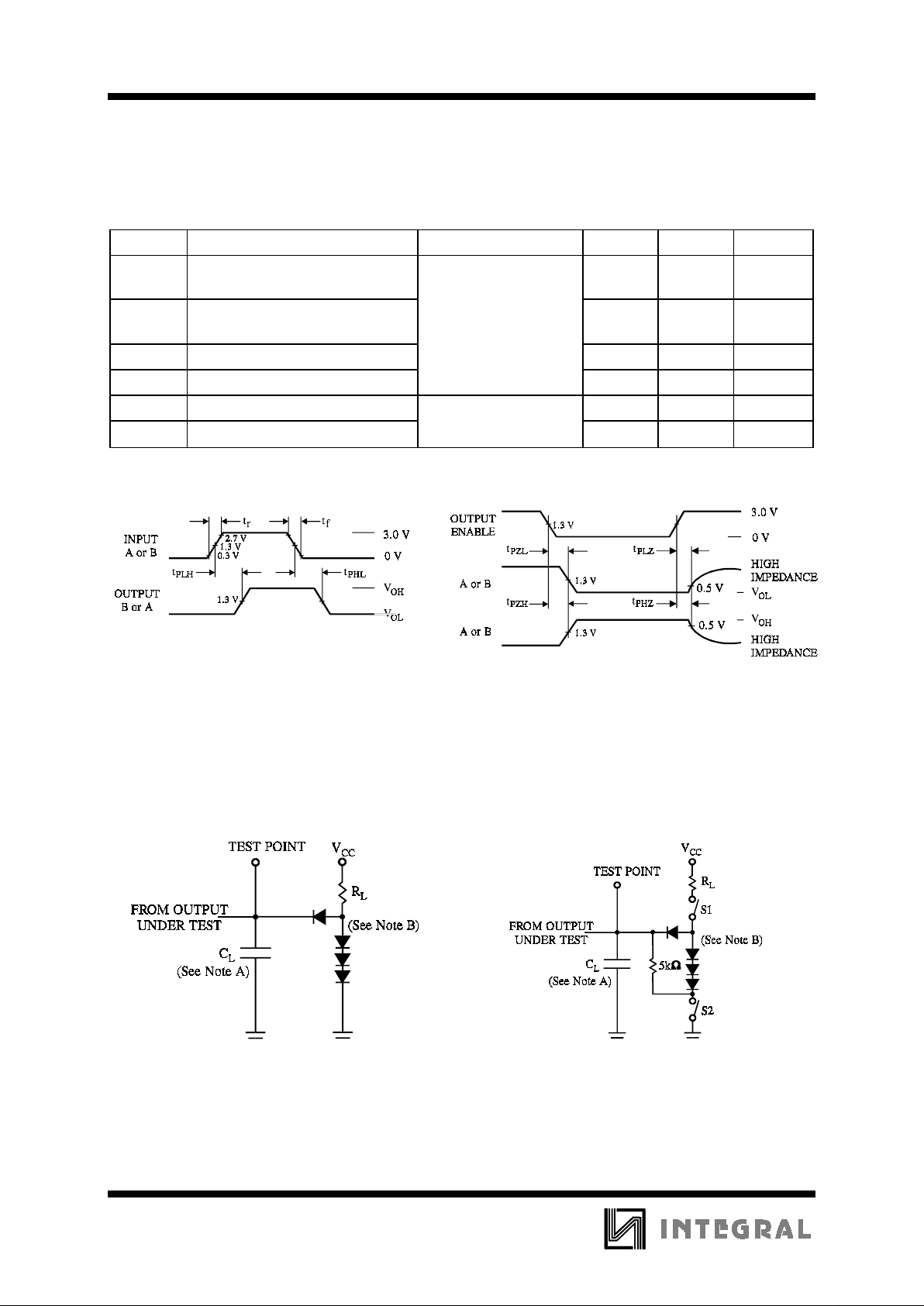
AC ELECTRICAL CHARACTERISTICS
(TA = 25°C, VCC = 5.0 V, tr = 15 ns,
t
f
= 6.0 ns)
Symbol Parameter Test Condition Min M ax Unit
t
PLH
Propagation Delay, Data to
Output
18 ns
t
PHL
Propagation Delay, Data to
Output
CL = 45 pF,
R
L
= 667
Ω
18 ns
t
PZH
Output Enable Time 23 ns
t
PZL
Output Enable Time 30 ns
t
PHZ
Output Disable Time CL = 5 pF 18 ns
t
PLZ
Output Disable Time
R
L
= 667
Ω
25 ns
t
PZL
- S1 closed, S2 opened
t
PZH
- S1 opened, S2 closed
t
PLZ
, t
PHZ
- S1 and S2 closed
Figure 1. Switching Waveforms
(See Figure 3)
Figure 2. Switching Waveforms
(See Figure 4)
NOTES A. CL includes probe and jig capacitance.
B. All diodes are 1N916 or 1N3064.
NOTES A. CL includes probe and jig capacitance.
B. All diodes are 1N916 or 1N3064.
Figure 3. Test Circuit
Figure 4. Test Circuit
Page 5
IN74LS244
5
Page 6
IN74LS244
6
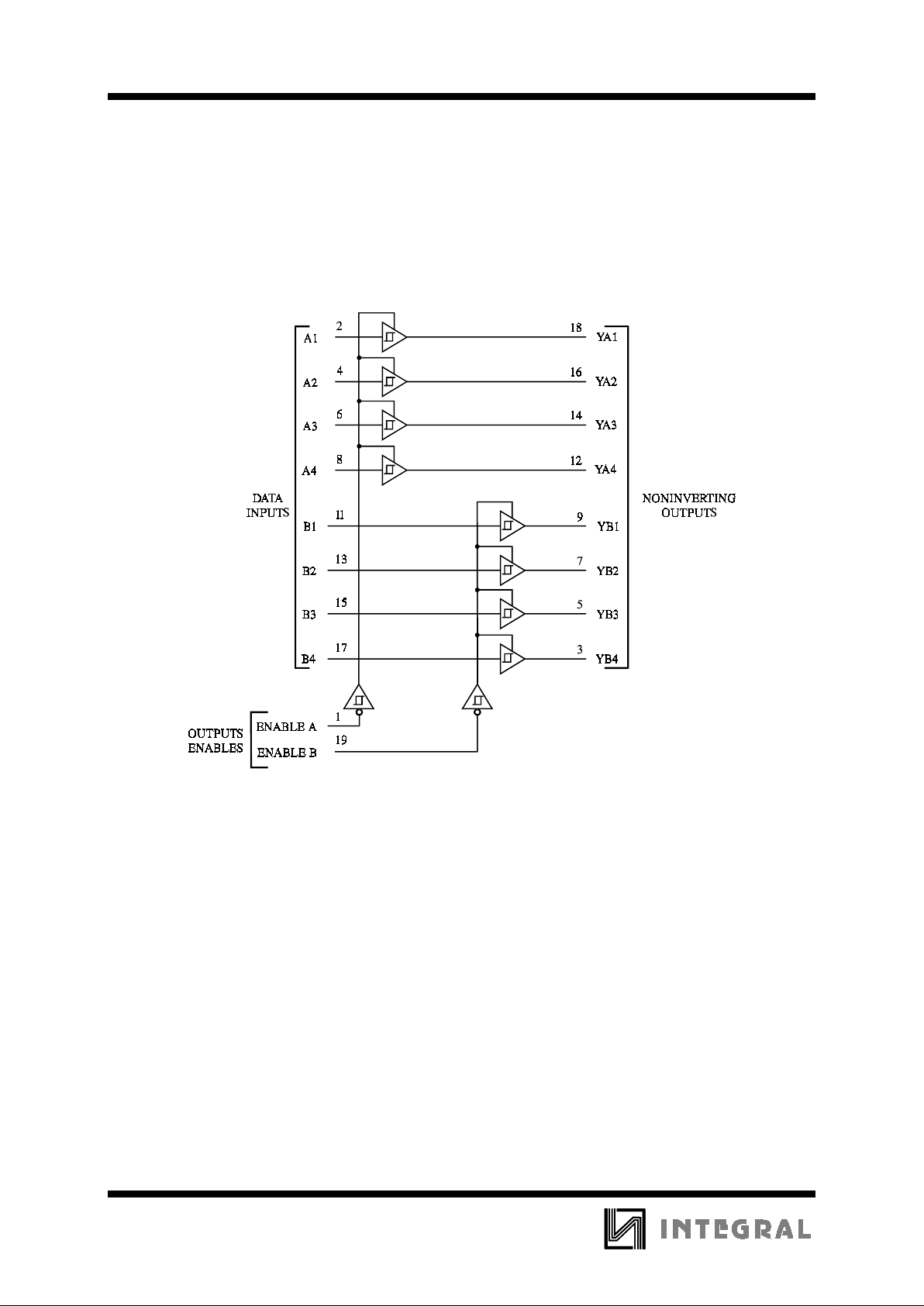
EXPANDED LOGIC DIAGRAM
 Loading...