

Page 1
TECHNICAL DATA
Phase-Locked Loop
IN74HC4046A
High-Performance Silicon-Gate CMOS
The device inputs are compatible with standard CMOS outputs;
with pullup resistors, they are compatible with LS/ALSTTL outputs.
The IN74HC4046A phase-locked loop contains three phase
comparators, a voltage-controlled oscillator (VCO) and unity gain opamp DEM
COMP
coupled to large voltage signals, or indirectly coupled (with a series
capacitor to small voltage signals). The self-bias circuit adjusts small
voltage signals in the linear region of the amplifier. Phase comparator
1 (an exclusive OR gate) provides a digital error signal PC1
maintains 90 degrees phase shift at the center frequency between SIG
and COMPIN signals (both at 50% duty cycle). Phase comparator 2
(with leading-edge sensing logic) provides digital error signals PC2
and PCP
COMP
an output signal VCO
voltage of input VCO
connected to pins C1A, C1B, R1 and R2. The unity gain op-amp output DEM
used where the VCO
the VCO and all on-amps to minimize standby power consumption.
Applications include FM and FSK modulation and demodulation, frequency synthesis and multiplication,
frequency discrimination, tone decoding, data synchronization and conditioning, voltage-to-frequency
conversion and motor speed control.
•
Low Power Consumption Characteristic of CMOS Device
•
Operating Speeds Similary to LS/ALSTTL
•
Wide Operating Voltage Range: 3.0 to 6.0 V
•
Low Input Current: 1.0 µA Maximum (except SIG
COMP
•
Low Quiescent Current: 80 µA Maximum (VC O disable d)
•
High Noise Immunity Characteristic of CMOS Devices
•
Diode Protection on all Inputs
. The comparators have two common signal inputs,
OUT
, and SIGIN. Input SIG
IN
and maintains a 0 degree phase shift between SIG
OUT
signals (duty cycle is immaterial). The linear VCO produces
IN
whose frequency is determined by the
OUT
IN
signal is needed but no loading can be tolerated. The inhibit input, when high, disables
IN
)
IN
and COMP
IN
can be used directly
IN
OUT
IN
signal and the capacitor and resistors
and
IN
and
OUT
and
IN
ORDERING INFORMATION
IN74HC4046AN Plastic
IN74HC4046AD SOIC
TA = -55° to 125° C for all packages
with an external resistor is
OUT
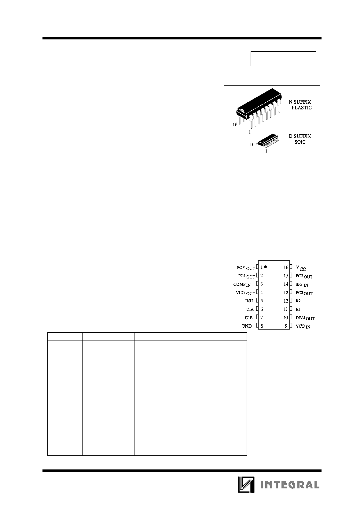
PIN ASSIGNMENT
Pin No. Symbol Name and Function
1PCP
2PC1
OUT
OUT
Phase Comparator Pulse Output
Phase Comparator 1 Output
3COMPINComparator Input
4VCO
OUT
VCO Output
5 INH Inhibit Input
6 C1A Capacitor C1 Connection A
7 C1B Cap acitor C1 Connection B
8 GND Ground (0 V) V
SS
9VCOINVCO Input
10 DEM
OUT
Demodulator Output
11 R1 Resistor R1 Connection
12 R2 Resistor R2 Connection
13 PC2
14 SIG
15 PC3
16 V
OUT
IN
OUT
CC
Phase Comparator 2 Output
Signal Input
Phase Comparator 3 Output
Positive Supply Voltage
480
Page 2
IN74HC4046A
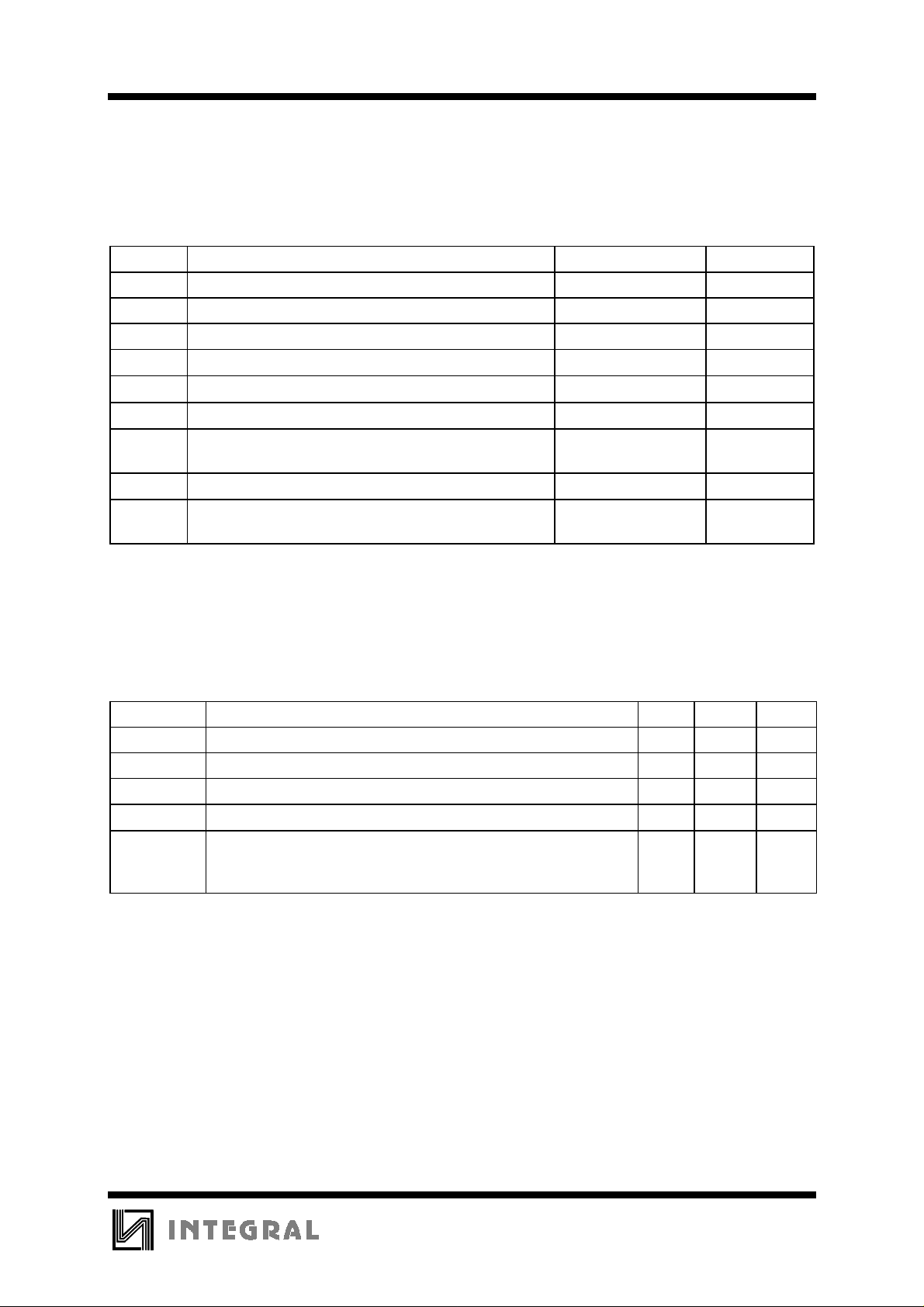
MAXIMUM RATINGS
*
Symbol Parameter Value Unit
V
CC
V
V
OUT
I
IN
I
OUT
I
CC
P
DC Supply Voltage (Referenced to GND) -0.5 to +7.0 V
DC Input Voltage (Referenced to GND) -1.5 to VCC +1.5 V
IN
DC Output Voltage (Referenced to GND) -0.5 to VCC +0.5 V
DC Input Current, per Pin
DC Output Current, per Pin
DC Supply Current, VCC and GND Pins
Power Dissipation in Still Air, Plastic DIP+
D
SOIC Package+
±
20
±
25
±
50
750
500
Tstg Storage Temperature -65 to +150
T
Lead Temperature, 1 mm from Case for 10 Seconds
L
260
(Plastic DIP or SOIC Package)
*
Maximum Ratings are those values beyond which damage to the device may occur.
Functional operation should be restricted to the Recommended Operating Conditions.
+Derating - Plastic DIP: - 10 mW/°C from 65° to 125°C
SOIC Package: : - 7 mW/°C from 65° to 125°C
mA
mA
mA
mW
°
C
°
C
RECOMMENDED OPERATING CONDITIONS
Symbol Parameter Min Max Unit
V
CC
V
CC
VIN, V
T
A
tr, t
f
This device c ontains p rote ction ci rcuitr y to guard a gainst damage d ue to high st atic voltages or electr ic
fields. However, precautions must be taken to avoid applications of any voltage higher than maximum rated
voltages to this high-impedance circuit. For proper operation, V
GND≤(V
Unused inputs must always be tied to an appropriate logic voltage level (e.g., either GND or V
Unused outputs must be left open.
DC Supply Voltage (Referenced to GND) VCO only 3.0 6.0 V
DC Supply Voltage (Referenced to GND) NON-VCO 2.0 6.0 V
DC Input Voltage, Output Voltage (Referenced to GND) 0 V
OUT
Operating Temperature, All Package Types -55 +125
Input Rise and Fall Time (Figure 1) VCC =2.0 V
IN
or V
OUT
)≤VCC.
V
V
IN
=4.5 V
CC
=6.0 V
CC
and V
should be constrained to the range
OUT
0
0
0
CC
1000
500
400
V
°
C
ns
CC
).
481
Page 3
IN74HC4046A
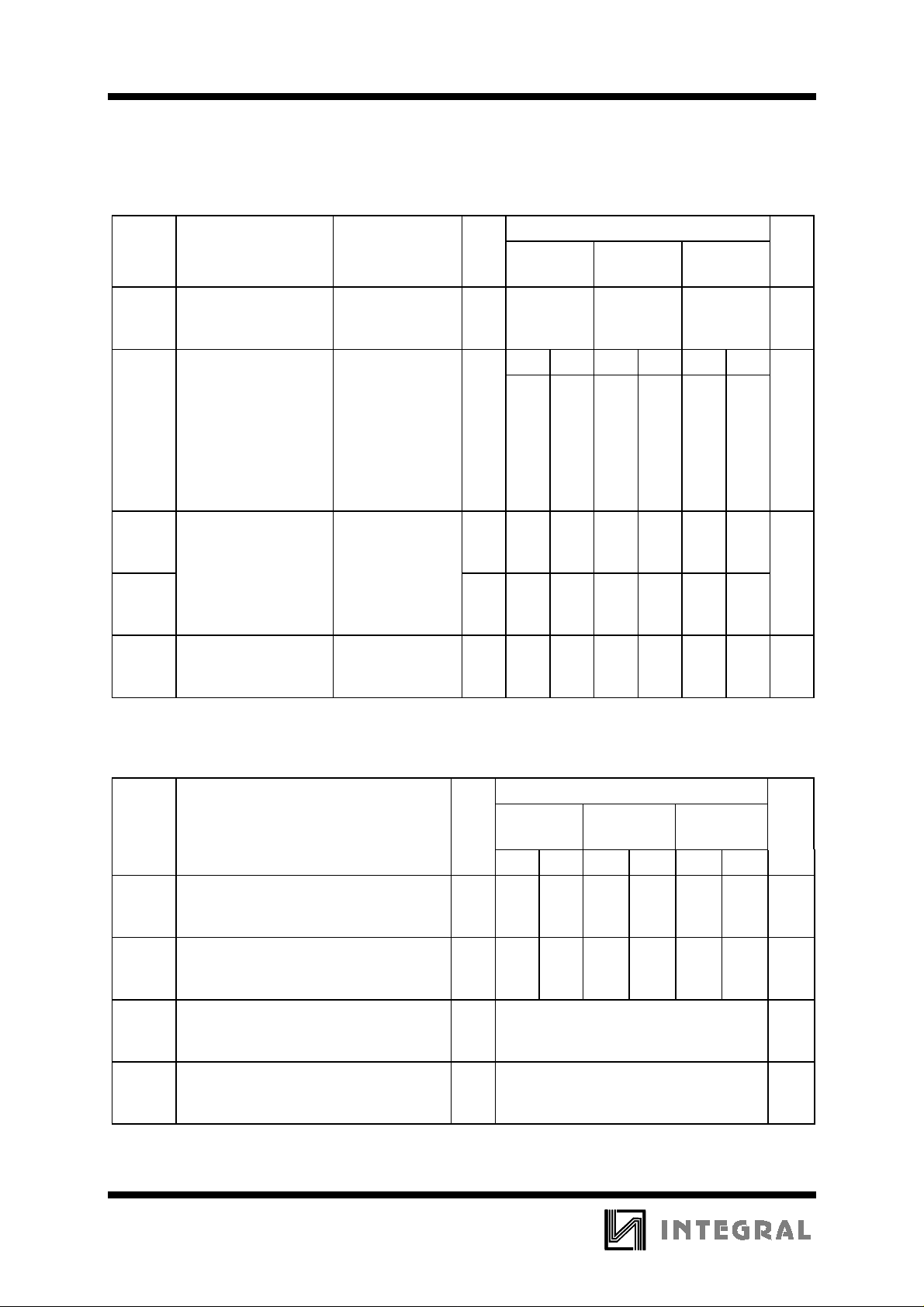
[Phase Comparator Section]
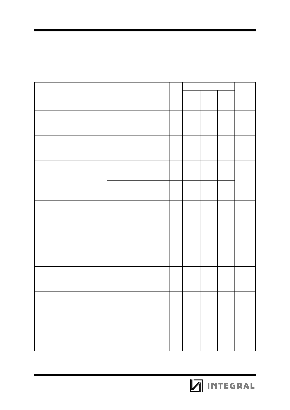
DC ELECTRICAL CHARACTERISTICS
(Voltages Referenced to GND)
V
Symbol Parameter Test Conditions V
V
Minimum High-Level
IH
Input Voltage DC
V
= 0.1 V or VCC-0.1 V
OUT
≤
I
20 µA
OUT
Coupled
SIG
, COMP
IN
V
Maximum Low -
IL
Level Input Voltage
IN
V
=0.1 V or VCC-0.1 V
OUT
≤
I
20 µA
OUT
DC Coupled
SIG
, COMP
IN
V
OH
Minimum High-Level
Output Voltage
PCP
OUT
V
OL
Maximum Low-Level
Output Voltage Q
PCP
OUT
I
IN
Maximum Input
, PCn
, PCn
OUT
OUT
IN
a-Qh
VIN=VIH or V
≤
I
OUT
VIN= VIH or V
≤
I
OUT
≤
I
OUT
VIN=VIH or V
≤
I
OUT
VIN= VIH or V
≤
I
OUT
≤
I
OUT
IL
20 µA
IL
4.0 mA
5.2 mA
IL
20 µA
IL
4.0 mA
5.2 mA
VIN=VCC or GND 2.0
Leakage Current
SIG
, COMP
IN
IN
2.0
4.5
6.0
2.0
4.5
6.0
2.0
4.5
6.0
4.5
6.0
2.0
4.5
6.0
4.5
6.0
3.0
4.5
6.0
I
OZ
I
CC
Maximum ThreeState Leakage
Current PC2
OUT
Maximum Quiescent
Supply Current
Output in High-Impedance
State
V
= VIL or V
IN
V
OUT=VCC
V
IN=VCC
=0µA
I
OUT
IH
or GND
or GND
6.0
6.0 4.0 40 160
(per Package)
(VCO disabled)
Pins 3,5 and 14 at
V
CC
Pin 9 at GND; Input
Leacage at
Pin 3 and 14 to be
excluded
CC
Guaranteed Limit
25 °C
to
≤
85
°
C
-55°C
1.5
3.15
4.2
0.5
1.35
1.8
1.9
4.4
5.9
3.98
5.48
0.1
0.1
0.1
0.26
0.26
±
±
±
18.0
±
30.0
±
3.0
7.0
0.5
1.5
3.15
4.2
0.5
1.35
1.8
1.9
4.4
5.9
3.84
5.34
0.1
0.1
0.1
0.33
0.33
±
±
±
23.0
±
38.0
±
4.0
9.0
5.0
≤
°
1.5
3.15
4.2
0.5
1.35
1.8
1.9
4.4
5.9
3.7
5.2
0.1
0.1
0.1
0.4
0.4
±
±
11.0
±
27.0
±
45.0
±
125
C
5.0
10
Unit
V
V
V
V
µ
A
µ
A
µ
A
482
Page 4
[Phase Comparator Section]
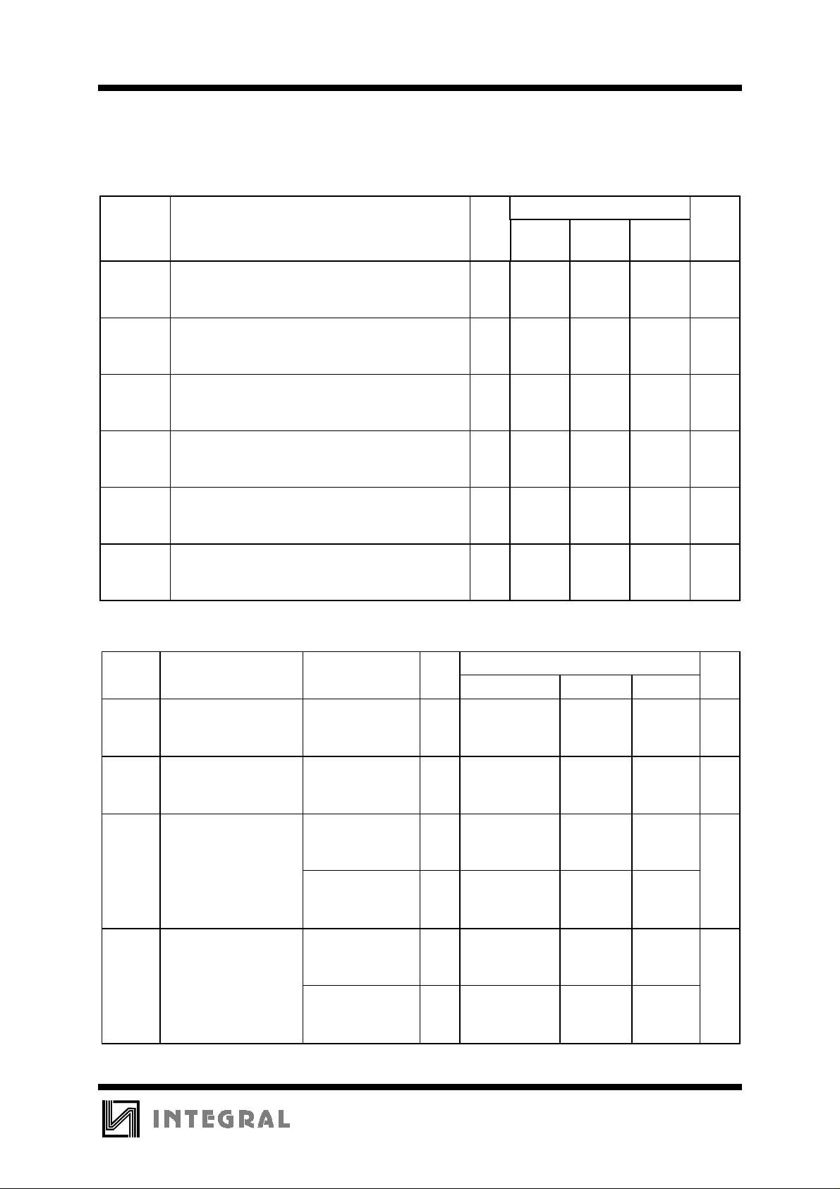
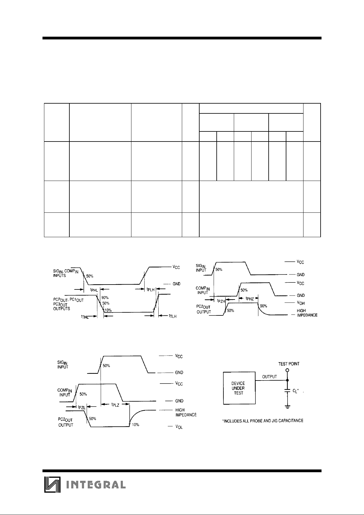
AC ELECTRICAL CHARACTERISTICS
IN74HC4046A
(CL=50pF,Input tr=tf=6.0 ns)
Symbol Parameter V
t
t
t
t
PLH
PLH
PLH
PLZ
, t
, t
, t
, t
Maximum Propagatio n Delay, SIGIN/COMPIN to
PHL
PC1
Maximum Propagatio n Delay, SIGIN/COMPIN to
PHL
PCP
Maximum Propagatio n Delay , SIGIN/COMPIN to
PHL
PC3
Maximum Propagatio n Delay , SIGIN/COMP
PHZ
Output Disable Time to PC2
(Figure 1)
OUT
(Figure 1)
OUT
(Figure 1)
OUT
OUT
IN
(Figures 2 and 3)
t
PZL
, t
Maximum Propagatio n Delay , SIGIN/COMP
PZH
Output Enable Time to PC2
OUT
IN
(Figures 2 and 3)
t
TLH
, t
Maximum Output Transition Time (Figure 1) 2.0
THL
[VCO Section]
DC ELECTRICAL CHARACTERISTICS
(Voltages Referenced to GND)
V
2.0
4.5
6.0
2.0
4.5
6.0
2.0
4.5
6.0
2.0
4.5
6.0
2.0
4.5
6.0
4.5
6.0
CC
Guaranteed Limit
25 °C to
-55°C
175
35
30
340
68
58
270
54
46
200
40
34
230
46
39
75
15
13
≤85°
C≤125°C
220
44
37
425
85
72
340
68
58
250
50
43
290
58
49
95
19
16
265
53
45
510
102
87
405
81
69
300
60
51
345
69
59
110
22
19
Unit
ns
ns
ns
ns
ns
ns
V
Symbol Parameter Test Conditions V
V
V
V
Minimum High-Level
IH
Input Voltage INH
Maximum Low -Level
IL
Input Voltage INH
Minimum High-Level
OH
Output Voltage
VCO
OUT
V
= 0.1 V or
OUT
V
-0.1 V
CC
≤
I
20 µA
OUT
V
=0.1 V or
OUT
V
-0.1 V
CC
≤
I
20 µA
OUT
VIN=VIH or V
≤
I
20 µA
OUT
IL
VIN= VIH or V
≤
I
4.0 mA
OUT
≤
I
5.2 mA
OUT
V
Maximum Low-Level
OL
Output Voltage
VCO
OUT
VIN=VIH or V
≤
I
20 µA
OUT
IL
VIN= VIH or V
≤
I
4.0 mA
OUT
≤
I
5.2 mA
OUT
3.0
4.5
6.0
3.0
4.5
6.0
3.0
4.5
6.0
IL
4.5
6.0
3.0
4.5
6.0
IL
4.5
6.0
CC
25 °C to-55°C
Guaranteed Limit
2.1
3.15
4.2
0.90
1.35
1.8
1.9
4.4
5.9
3.98
5.48
0.1
0.1
0.1
0.26
0.26
≤85°
2.1
3.15
4.2
0.90
1.35
1.8
1.9
4.4
5.9
3.84
5.34
0.1
0.1
0.1
0.33
0.33
≤
C
125°C
2.1
Unit
V
3.15
4.2
0.90
V
1.35
1.8
1.9
V
4.4
5.9
3.7
5.2
0.1
V
0.1
0.1
0.4
0.4
(continued)
483
Page 5
IN74HC4046A
[VCO Section]
DC ELECTRICAL CHARACTERISTICS
(Voltages Referenced to GND) - continued
V
Symbol Parameter Test Conditions V
I
Maximum Input
IN
VIN =V
or GND 6.0 0.1 1.0 1.0
cc
Leakage Current INH,
VCO
IN
V
VCOIN
Operating Voltage
Range at VCO
IN
over
the range specified for
INH= V
IL
3.0
4.5
6.0
R1; For linearity see
Fig.13A, Parallel value
of R1 and R2 should
be >2.7 k
Ω
R1 Resistor Range 3.0
4.5
6.0
R2 3.0
4.5
6.0
C1 Capacitor Range 3.0
4.5
6.0
CC
25 °C to
Guaranteed Limit
≤85°
C
-55°C
Min Max Min Max Min Max
0.1
1.0
0.1
1.0
0.1
2.5
0.1
2.5
0.1
4.0
0.1
4.0
300
3.0
300
3.0
300
3.0
300
3.0
300
3.0
300
3.0
3.0
300
3.0
300
3.0
300
3.0
300
3.0
300
3.0
300
No
40
Li-
40
mit
40
≤
0.1
0.1
0.1
3.0
3.0
3.0
3.0
3.0
3.0
125°C
300
300
300
300
300
300
1.0
2.5
4.0
Unit
µ
A
V
Ω
k
pF
[VCO Section]
AC ELECTRICAL CHARACTERISTICS
Symbol Parameter V
∆
∆
fVCO
∂
VCO
Frequency Stability with Temperature
f/T
Changes (Figures 11A,B,C)
fo VCO Center Frequency
(Duty Factor = 50%)
(Figures 12A,B,C)
VCO Frequency Linearity 3.0
Duty Factor at VCO
OUT
(CL=50pF,Input tr=tf=6.0 ns)
V
CC
25 °C to
Guaranteed Limit
≤85°
-55°C
Min Max Min Max Min Max
3.0
4.5
6.0
3.0
4.5
6.0
3
11
13
See Figures 13A,B %
4.5
6.0
3.0
Typical 50% %
4.5
6.0
C
≤
125°C
Unit
%/K
MHz
484
Page 6
[Demodulator Section]
DC ELECTRICAL CHARACTERISTICS
IN74HC4046A
V
Symbol Parameter Test Conditions V
RS Resistor Range
At RS > 300 k
the Leakage
Current can
3.0
Ω
4.5
6.0
Influence
VDEM
OUT
V
Offset Voltage VCO
OFF
to VDEM
OUT
VI = VVCO
IN
1/2 V
; Values
CC
IN
taken over RS
3.0
=
4.5
6.0
Range
RD Dynamic Output
Resistance at DEM
OUT
VDEM
1/2 V
CC
OUT
=
3.0
4.5
6.0
CC
25 °C to
Guaranteed Limit
≤85°
C
-55°C
Min Max Min Max Min Max
50
300
50
300
50
300
See Figure 10 mV
Typical 25
ΩΩ
≤
125°C
Unit
Ω
k
Figure 1. Switching Waveforms Figure 2. Switching Waveforms
Figure 3. Switching Waveforms Figure 4. Test Circuit
485
Page 7
IN74HC4046A
DETAILED CIRCUIT DESCRIPTION
Voltage Controlled Oscillator/Demodulator Output
The VCO requires two or three external
components to operate. These are R1, R2, C1. Resistor
R1 and Capacitor C1 are selected to determine the
center frequency of the VCO (see typical performance
curves Figure 12). R2 can be used to set the offset
frequency with 0 volts at VCO input. For example, if
R2 is decreased, the offset frequency is increased. If
R2 is omitted the VCO range is from 0 Hz. By
increasing the value of R2 the lock range of the PLL is
increased and the gain (volts/Hz) is decreased. Thus,
for a narrow lock range, large swings on the VCO
input will cause less frequency variation.
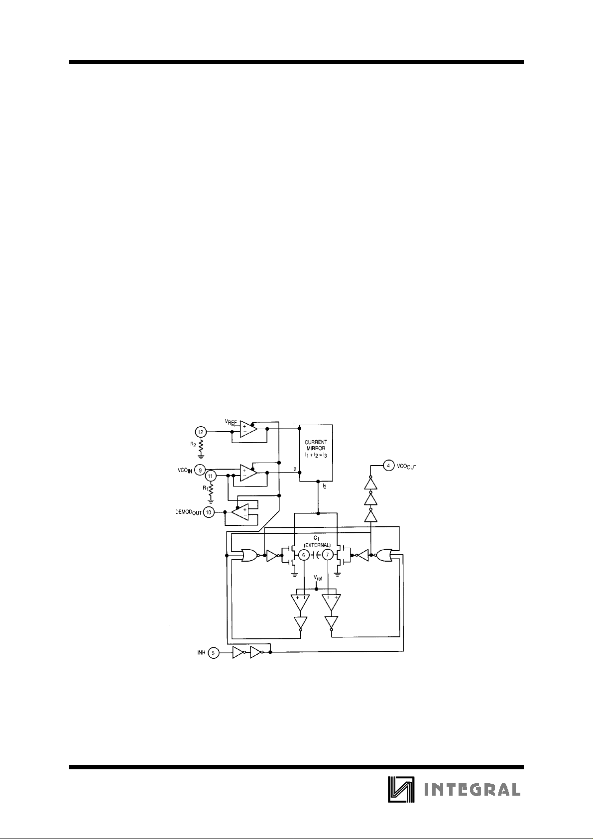
Internally, the resistors set a current in a current
mirror, as shown in Figure 5. The mirrored current
drives one side of the capacitor. Once the voltage
across the capacitor charges up to V
comparators, the oscillator logic flips the capacitor
which causes the mirror to change the opposite side of
of the
ref
the capacitor. The output from the internal logic is
then taken to VCO output (Pin4).
The input to the VCO is a very high impedance
CMOS input and thus will not load down the loop
filter, easing the filters design. In order to make
signals at the VCO input accessible without degrading
the loop performance, the VCO input voltage is
buffered through a unity gain Op-amp, to Demod
Output. This Op-amp can drive loads of 50K ohms or
more and provides no loading effects to the VCO input
voltage (see Figure 10).
An inhibit input is provided to allow disabling
of the VCO and all Op-amps (see Figure 5). This is
useful if the internal VCO is not being used. A logic
high on inhibit disables the VCO and all Op-amps,
minimizing standby power consumpti on.
The output of the VCO is a standard high speed
CMOS output with an eq uivalent LS-TTL fan out o f
10. The VCO output is approximately a square wave.
This output can either directly feed the COMP
phase comparators or feed external prescalers
(counters) to enable frequency synthesis.
of the
IN
486
Figure 5. Logic Diagram for VCO
Page 8
IN74HC4046A
Phase Comparators
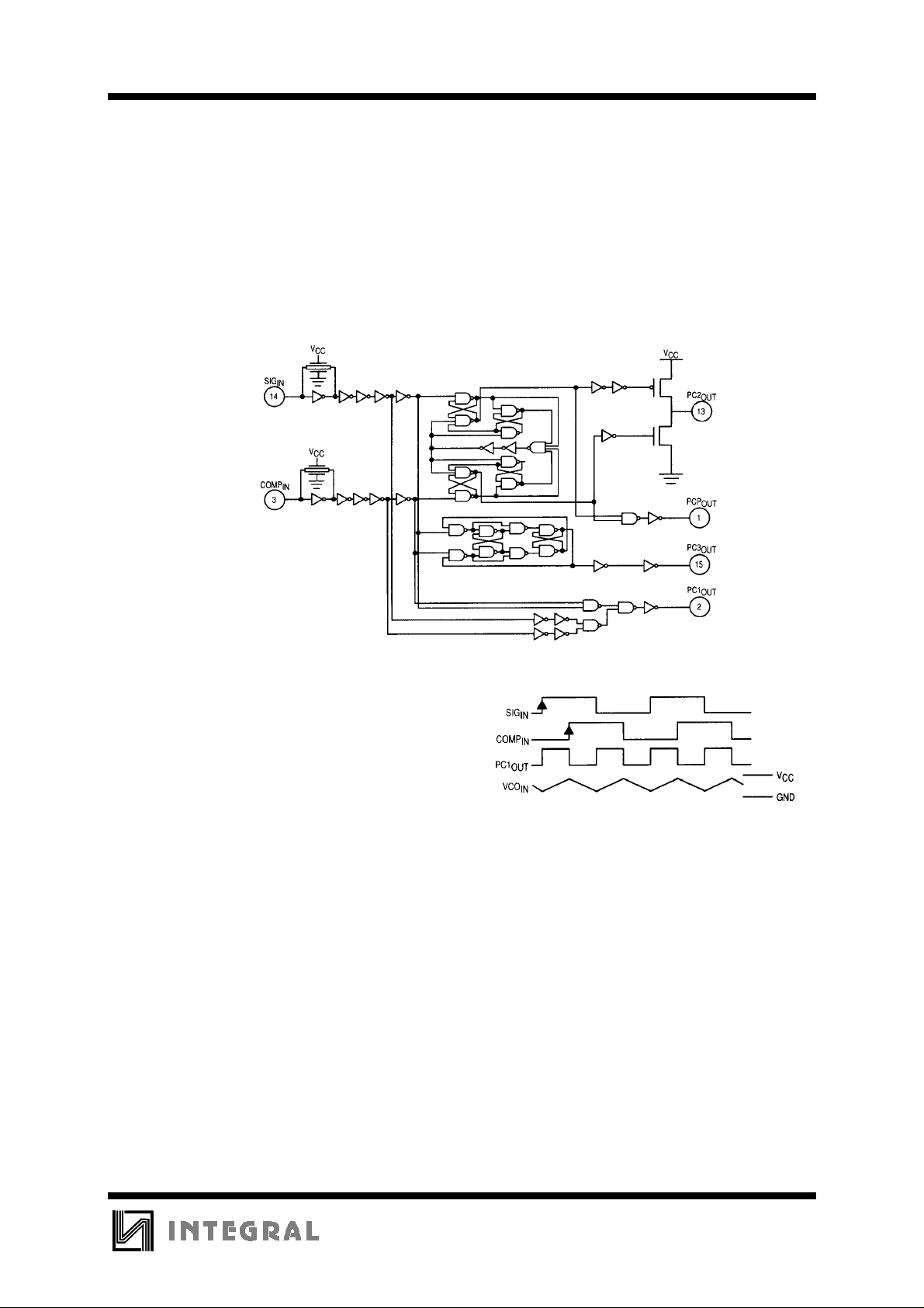
All three phase comparators have two inputs,
SIG
and COMPIN. The SIGIN and COMPIN have a
IN
special DC bias network that enables AC coupling of
input signals. If the signals are not AC coupled,
standard IN74HC input levels are required. Both input
structures are shown in Figure 6. The outputs of these
comparators are essentially standard IN74HC outputs
(comparator 2 is TRI-STATEABLE). In normal
operation V
and ground vo ltage le vels are fed to the
CC
loop filter. This differs from some phase detectors
which supply a current to the loop filter and should be
considered in the design.
Figure 6. Logic Diagram for Phase Comparators
Phase Comparator 1
This comparator is a simple XOR gate similar
to the IN74HC86. Its operation is similar to an
overdriven balanced modulator. To maximize lock
range the input frequencies must have a 50% duty
cycle. Typical input and output waveforms are shown
in Figure 7. The output of the phase detector feeds the
loop filter which averages the output voltage. The
frequency range upon which the PLL will lock onto if
initially out of lock is defined as the capture range.The
capture range for phase detector 1 is dependent on the
loop filter design. The capture range can be as large as
the lock range, which is equal to the VCO frequency
range.
To see how the detector operates, refer to
Figure 7. When two squa re wave signals ar e a pp li ed to
this comparator, an output waveform (whose duty
cycle is dependent on the phase difference between the
two signals) results. As the phase difference increases,
the output duty cycle increases and the voltage after
the loop filter increases. In order to achieve lock when
the PLL input frequency increases, the VCO input
voltage must increase and the phase difference
between COMP
frequency equal to f
and SIGIN will increase. At an input
IN
, the VCO input is at 0 V
min
Figure 7. Typical Waveforms for PLL Using
Phase Comparator 1
This requires the phase detector output to be
grounded; hence, the two input signals must be in
phase. When the input frequency is f
input must be V
and the phase detector inputs must
CC
, the VCO
max
be 180 degrees out of phase.
The XOR is more susceptible to locking onto
harmonics of the SIG
than the digital phase detector
IN
2. For instance, a signal 2 times the VCO frequency
results in the same output duty cycle as a signal equal
to the VCO frequency. The difference is that the
output frequency of the 2f example is twice that of the
other example. The loop filter and VCO range should
be designed to prevent locking on to harmonics.
487
Page 9
IN74HC4046A
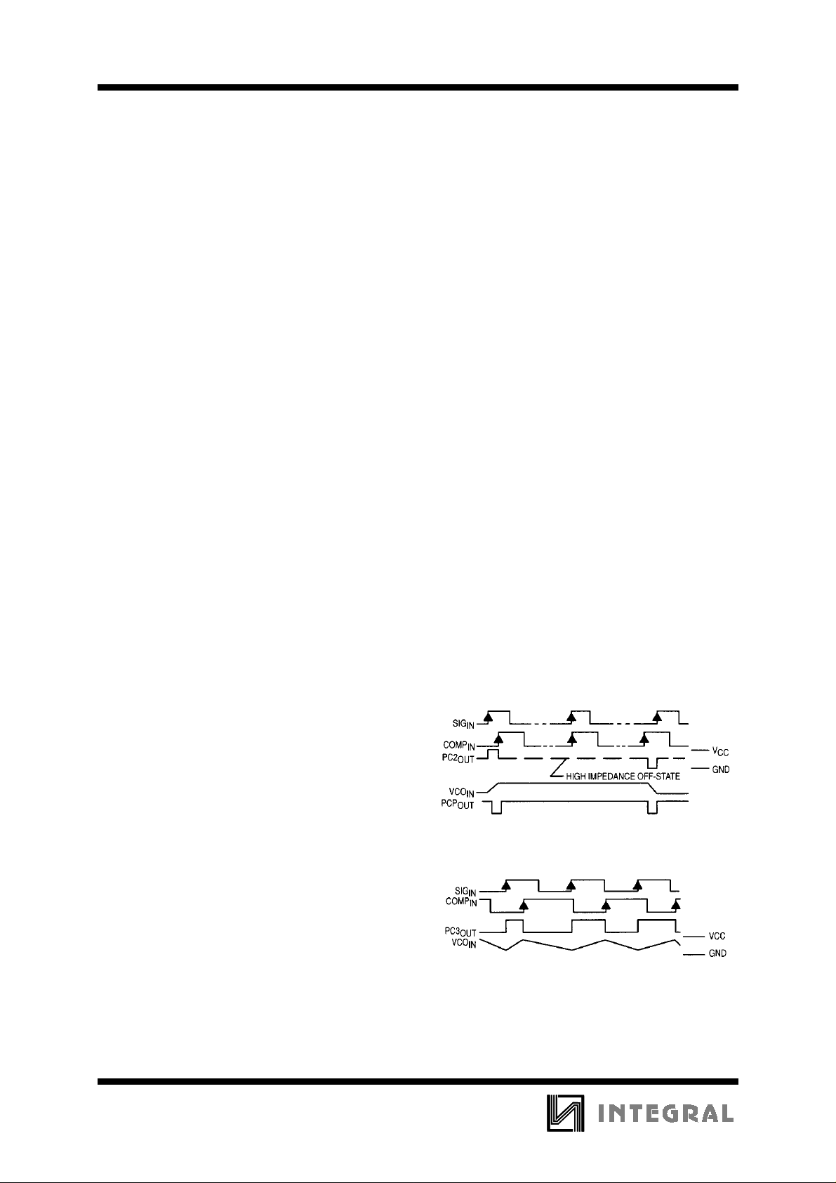
Phase Comparator 2
This detector is a digital memory network. It
consists of four flip-flops and some gating logic, a
three state output and a phase pulse output as shown in
Figure 6. This comparator acts only on the positive
edges of the input signals and is independent of duty
cycle.
Phase comparator 2 operates in such a way as
to force the PLL into lock with 0 phase difference
between the VCO output and the signal input positive
waveform edges. Figure 8 shows some typical loop
waveforms. First assume that SIG
COMP
. This means that the VCO’s frequency must
IN
is leading the
IN
be increased to bring its leding edge into proper phase
alignment. Thus the phase detector 2 output is set
high. This will cause the loop filter to charge up the
VCO input, increasing the VCO frequency. Once the
leading edge of the COMP
is detected, the output
IN
goes TRI-STATE holding the VCO input at the loop
filter voltage. If the VCO still lags the SIG
then the
IN
phase detector will again charge up the VCO input for
the time between the leading edges of both waveforms.
If the VCO leads the SIG
then when the
IN
leading edge of the VCO is seen; the output of the
phase comparator goes low. This discharges the loop
filter until the leading edge of the SIG
is detected at
IN
which time the output disables itself again. This has
the effect of slowing down the VCO to again make the
rising edges of both waveforms coincidental.
When the PLL is out of lock, the VCO will be
running either slower o r faster than the SIG
. If it is
IN
running slower the phase detector will see more SIG
rising edges and so the output of the phase comparator
will be high a majority of the time, raising the VCO’s
frequency. Conversely, if the VCO is running faster
than the SIG
, the output of the detector will be low
IN
most of the time and the VCO’s output frequency will
be decreased.
As one can see, when the PLL is locked, the
output of phase comparator 2 will be disabled except
for minor corrections at the leading edge of the
waveforms. When PC
is TRI-STATED, the PCP
2
output is high. This output can be used to determine
when the PLL is in the locked condition.
This detector has several interesting
characteristics. Over the entire VCO frequency range
there is no phase difference between the COMP
the SIG
. The lock range of the PLL is the same as
IN
IN
and
the capture range. Minimal power was consumed in
the loop filter since in lock the detector output is a
high impedance. When no SIG
is present, the
IN
detector will see only VCO leading edges, so the
comparator output will stay low, forcing the VCO to
f
.
min
Phase comparator 2 is more susceptible to
noise, causing the PLL to unlock. If a noise pulse is
seen on the SIG
positive edge of the SIG
, the comparator treats it as another
IN
and will cause the output to
IN
go high until the VCO leding edge is see, potentially
for an entire SIG
period. This would cause the VCO
IN
to speed up during that time. When using PC
output of that phase detector would be disturbed for
only the short duration of the noise spike and would
cause less upset.
Phase Comparator 3
This is positive edge-triggered sequential phase
detector using an RS flip-flop as shown in Figure 6.
When the PLL is using this comparator, the loop is
controlled by positive signal transitions and the duty
factors of SIG
and COMPIN are not important. It has
IN
some similar characteristics to the edge sensitive
comparator. To see how this detector works, assume
input pulses are applied to the SIGN
as shown in Figure 9. When the SIGN
COMP
, the flop is set. This will charge the loop
IN
and COMPIN’s
IN
IN
filter and cause the VCO to speed up, bringing the
comparator into phase with the SIG
between SIG
and is 180° at f
than for PC
and COMPIN varies from 0° to 360
IN
. The voltage swing for P C3 is greater
o
but consequently has more ripple in the
2
signal to the VCO .Whe n no SIG
will be forced to f
as opposed to fmin when PC2 is
max
. The phase angle
IN
is present the VCO
IN
used.
The operating characteristics of all three phase
comparators tors should be compared to the
requirement of the system design and the appropriate
IN
one should be used.
Figure 8. Typical Waveforms for PLL Using
Phase Comparator 2
Figure 9. Typical Waveforms for PLL Using
Phase Comparator 3
, the
1
leads the
°
488
Page 10
IN74HC4046A
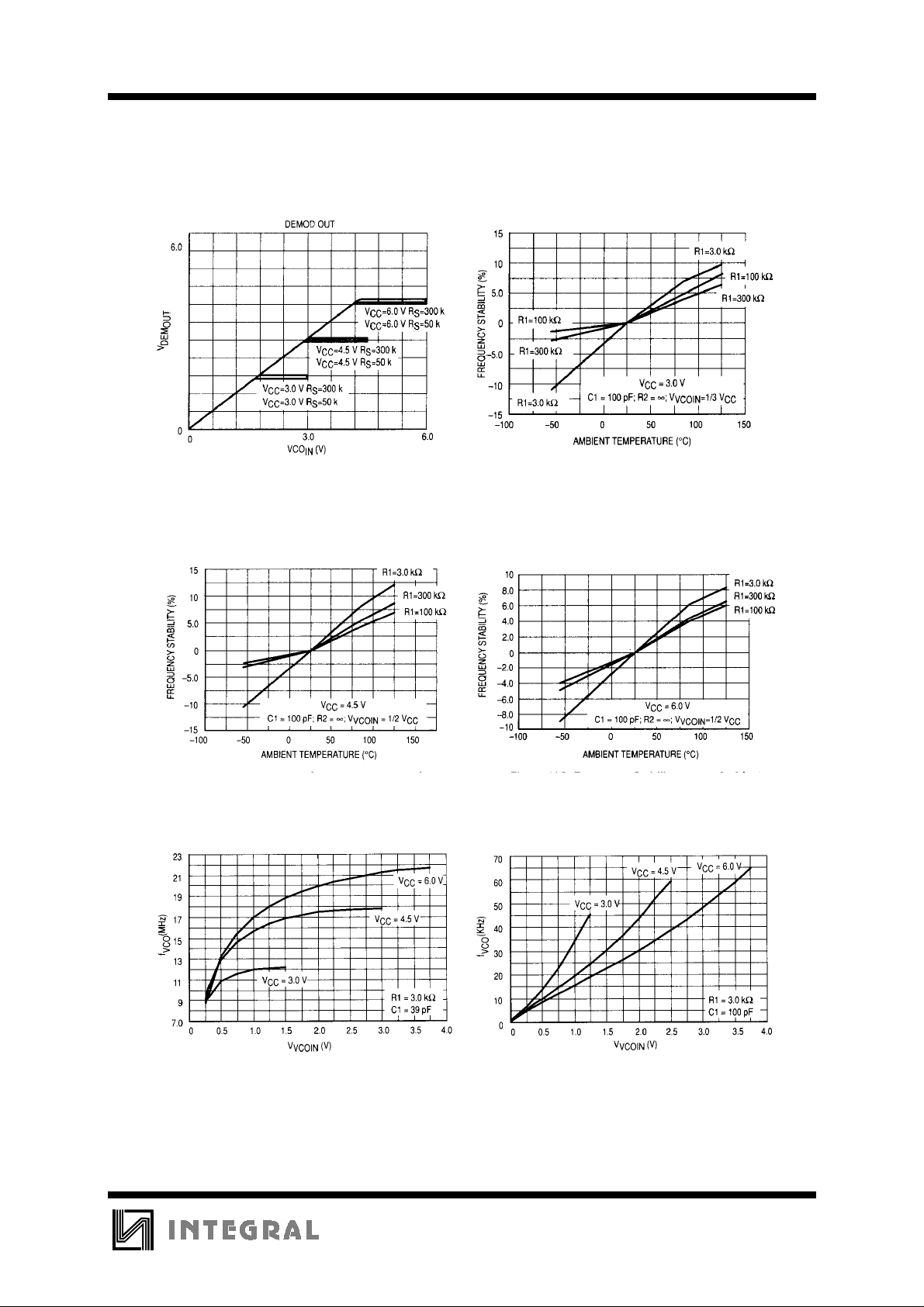
Figure 10. Offset Voltage at Demodulator Output
as a Function of VCO
and R
IN
S
Figure 11B. Frequency Stability versus Ambient
Temperature: V
= 4.5 V
CC
Figure 11A. Frequency Stability versus Ambient
Temperature: V
= 3.0 V
CC
Figure 11C. Frequency Stability versus Ambient
Temperature: VCC = 6.0 V
Figure 12A. VCO Frequency (f
the VCO Input Voltage (V
) as a Function of
VCO
)
VCOIN
Figure 12B. VCO Frequency (f
the VCO Input Voltage (V
) as a Function of
VCO
)
VCOIN
489
Page 11
IN74HC4046A
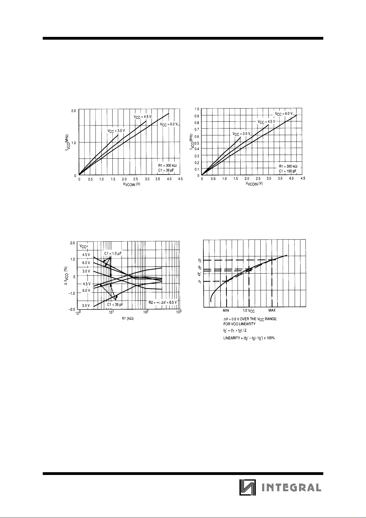
Figure 12C. VCO Frequency (f
the VCO Input Voltage (V
) as a Function of
VCO
)
VCOIN
Figure 13A. Frequency Linearity versus R1,C1 and
V
CC
Figure 12D. VCO Frequency (f
) as a Function of
VCO
the VCO Input Voltage (V
Figure 13B. Definition of VCO Frequency
Linearity)
VCOIN
)
490
 Loading...