

Page 1
TECHNICAL DATA
1
Octal D-Type 3-State Transparent Latch
These 8-bit registers feature totem-pole 3-State outputs designed
specifically for driving highly-capacitive or relatively low-impedance
loads. The high-impedance state and increased high-logic-level drive
provide these registers with the capability of being connected directly
to and driving the bus lines in a bus-organized system without need for
interface or pull-up components. They are particularly attractive for
implementing buffer registers, I/O ports, bidirectional bus drivers, and
working registers.
The eight latches of the ALS373 are transparent D-type latches.
While the Latch Enable is high the Q outputs will follow the data(D)
inputs. When the enable is taken low the output will be latched at the
level of the data that was set up.
A buffered output control input can be used to place the eight
outputs in either a normal logic state (high or low logic levels) or a
high-impedance state. In the high-impedance state the outputs neither
load nor drive the bus lines significanty.
The output control does not affect the internal operation of the
latches. That is, the old data can be retained or new data can be entered
even while the outputs are off.
•
Switching specificatio ns at 50 pF
•
Switching specifications guaranteed over full temperature and
V
CC
range
•
Functionally and pin for pin compatible with LS TTL counterpart
•
Improved AC performance over LS373 at approximately half the
power
•
TRI-STATE buffer-type outputs drive bus lines directly
IN74ALS373
ORDERING INFORMATION
IN74ALS373N Plastic
IN74ALS373DW SOIC
TA = -10° to 70° C
for all packages
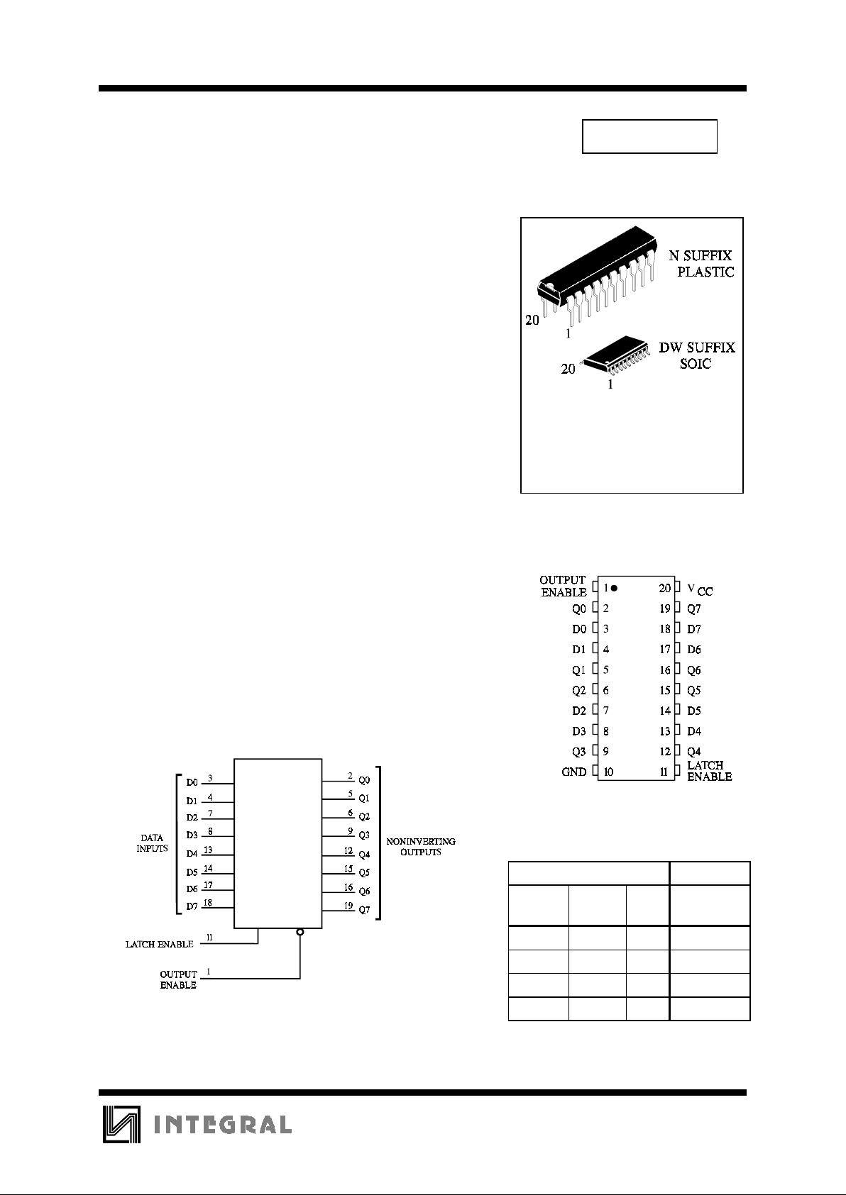
FUNCTION TABLE
Inputs Output
Output
Enable
Latch
Enable
DQ
LHHH
LHL L
L L X No Change
HXX Z
X = Don’t Care
Z = High Impedance
PIN ASSIGNMENT
LOGIC DIAGRAM
PIN 20=V
CC
PIN 10 = GND
Page 2
IN74ALS373
2
MAXIMUM RATINGS
*
Symbol Parameter Value Unit
V
CC
Supply Voltage 7.0 V
V
IN
Input Voltage 7.0 V
V
OUT
Output Voltage (Referenced to GND) 5.5 V
Tstg Storage Temperature Range -65 to +150
°
C
*
Maximum Ratings are those values beyond which damage to the device may occur.
Functional operation should be restricted to the Recommended Operating Conditions.
RECOMMENDED OPERATING CONDITIONS
Symbol Parameter Min Max Unit
V
CC
Supply Voltage 4.5 5.5 V
V
IH
High Level Input Voltage 2.0 V
V
IL
Low Level Input Voltage 0.8 V
I
OH
High Level Output Current -2.6 mA
I
OL
Low Level Output Current 24 mA
T
A
Ambient Temperature Range -10 +70
°
C
DC ELECTRICAL CHARACTERISTICS
over full operating conditions
Guaranteed Limit
Symbol Parameter Test Conditions Min Max Unit
V
IK
Input Clamp Voltage VCC = min, IIN = -18 mA -1.5 V
V
OH
High Level Output Voltage VCC = min, IOH = -0.4 mA 2.5 V
VCC = min, IOH = -2.6 mA 2.4
V
OL
Low Level Output Voltage VCC = min, IOL = 12 mA 0.4 V
VCC = min, IOL = 24 mA 0.5
I
OZH
Output Off Current HIGH VCC = max, V
OUT
= 2.7 V 20
µ
A
I
OZL
Output Off Current LOW VCC = max, V
OUT
= 0.4 V -20
µ
A
I
IH
High Level Input Current VCC = max, VIN = 2.7 V 20
µ
A
VCC = max, VIN = 7.0 V 0.1 mA
I
IL
Low Level Input Current VCC = max, VIN = 0.4 V -0.1 mA
I
O
Output Short Circuit Current VCC = max, VO = 2.25 V -30 -112 mA
I
CC
Supply Current VCC = max Outputs Low 16 mA
Outputs High 25
3-State
(High Z)
27
Page 3
IN74ALS373
3
AC ELECTRICAL CHARACTERISTICS
over full operating conditions
(VCC = 5.0 V±10%, CL = 50 pF, RL1 = RL2 = 500 Ω, Input tr = tf = 2.0 ns)
Guaranteed Limit
Symbol Parameter Min Max Unit
t
PLH
Propagation Delay Time, Data to Any Q 12 ns
t
PHL
Propagation Delay Time, Data to Any Q 16 ns
t
PLH
Propagation Delay Time, Latch Enable to Any Q 22 ns
t
PHL
Propagation Delay Time, Latch Enable to Any Q 23 ns
t
PZH
Propagation Delay Time, Output Enable to Any Q 20 ns
t
PZL
Propagation Delay Time, Output Enable to Any Q 18 ns
t
PHZ
Propagation Delay Time, Output Enable to Any Q 40 ns
t
PLZ
Propagation Delay Time, Output Enable to Any Q 30 ns
t
w
Enable Width 10 ns
t
su
Setup Time 10 ns
t
h
Hold Time 7 ns
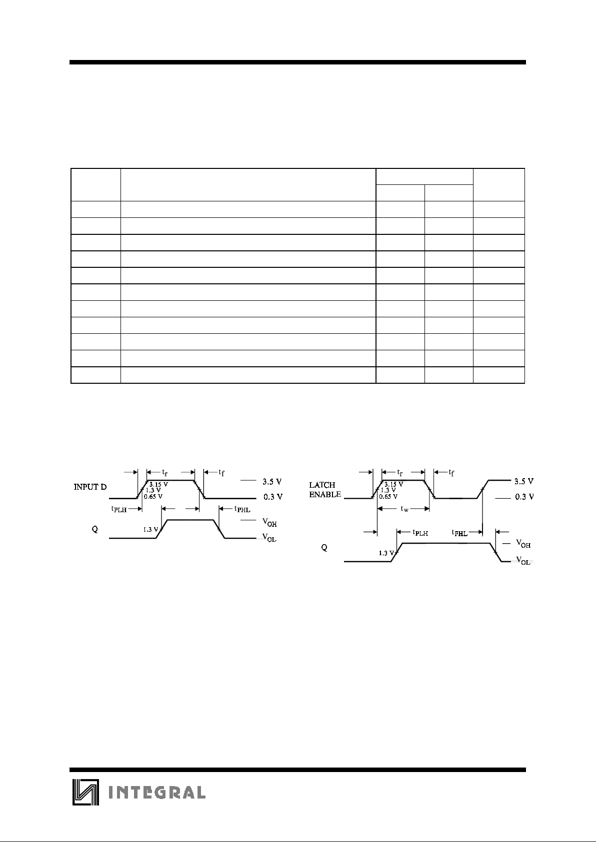
Figure 1. Switching Waveforms Figure 2. Switching Waveforms
Page 4
IN74ALS373
4
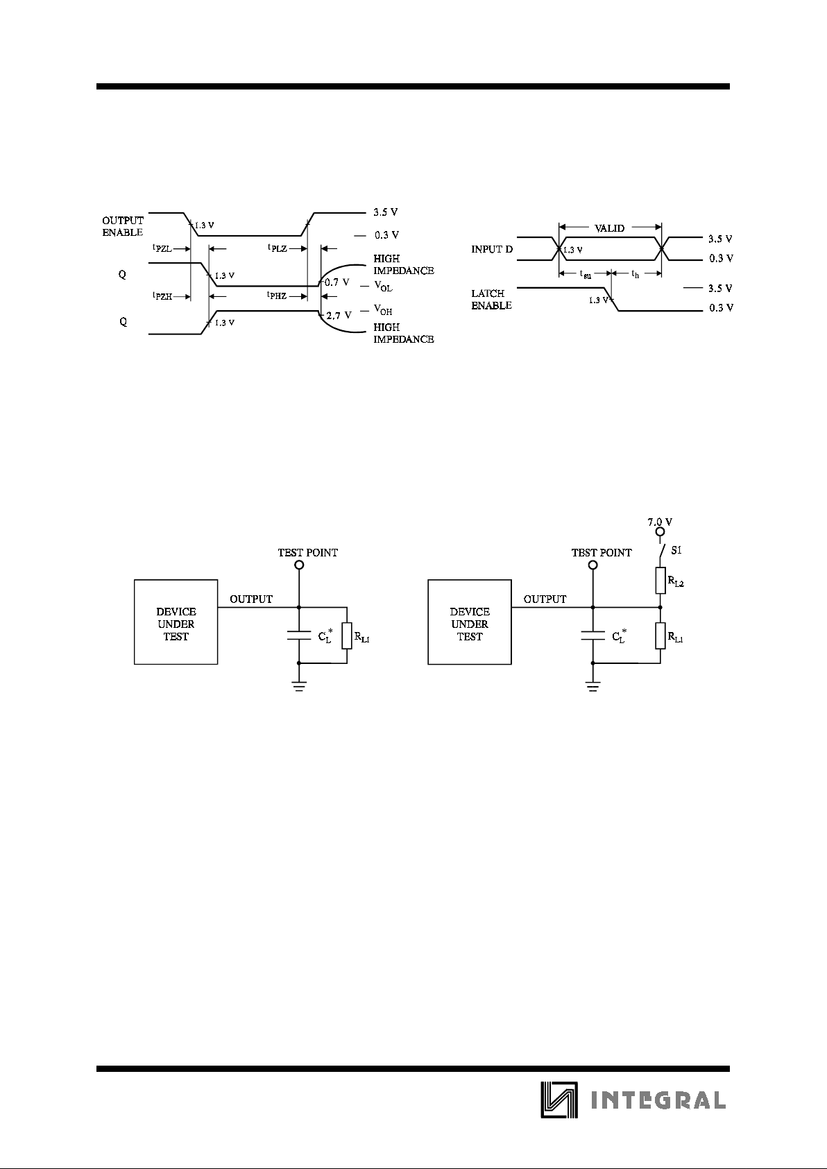
t
PZL
, t
PLZ
- S1 closed
t
PZH
, t
PHZ
- S1 opened
Figure 3. Switching Waveforms Figure 4. Switching Waveforms
* Includes all probe and jig capacitance. * Includes all probe and jig capacitance.
Figure 3. Test Circuit Figure 4. Test Circuit
 Loading...