

Page 1
TECHNICAL DATA
1
Synchronous 4 Bit Counters; Binary,
Direct Reset
This synchronous, presettable counter features an internal carry
look-ahead for application in high-speed counting designs.
Synchronous operation is provided by having all flip-flops clocked
simultaneously so that the outputs change conicident with each other
when so instructed by the count-enable inputs and internal gating.
This mode of operation eliminates the output counting spikes that
are normally associated with asynchronous (ripple clock) counters. A
buffered clock input triggers the four flip-flops on the rising (positivegoing) edge o f the clock input wave form.
This counter is fully programmable; that is the outputs may be
preset to either level. As presetting is synchronous setting up a low
level at the load input disables the counter and causes the outputs to
agree with the setup data after the next clock pulse regardless of the
levels of the enable inputs.
The carry look-ahead circuitry provides for cascading counters for
n-bit synchronous applications without additional gating. Instrumental
in accomplishiing this function are two counter-enable inputs and a
ripple carry output. Both countenable inputs (ENABLE P and
ENABLE T) must be high to count, and ENAB LE T is fed forward
to enable the ripple carry output. The ripple carry output thus
enabled will produce a high-level output pulse with a duration
approximately equal to the high level portion of the Q
A
output. The
high-level overflow ripple carry pulse can be enable successive
cascaded stages. Transitions at the ENPor ENT are allowed
regardless of the level of the clock input.
•
Internal Look-Ahead for Fast Counting
•
Carry Output for n-Bit Cascading
•
Synchronous Counting
•
Synchronously Programmable
•
Load Control Line
•
Diode-Clamped Inputs
IN74ALS161A
ORDERING INFORMATION
IN74ALS161AN Plastic
IN74ALS161AD SOIC
TA = -10° to 70° C for all
packages
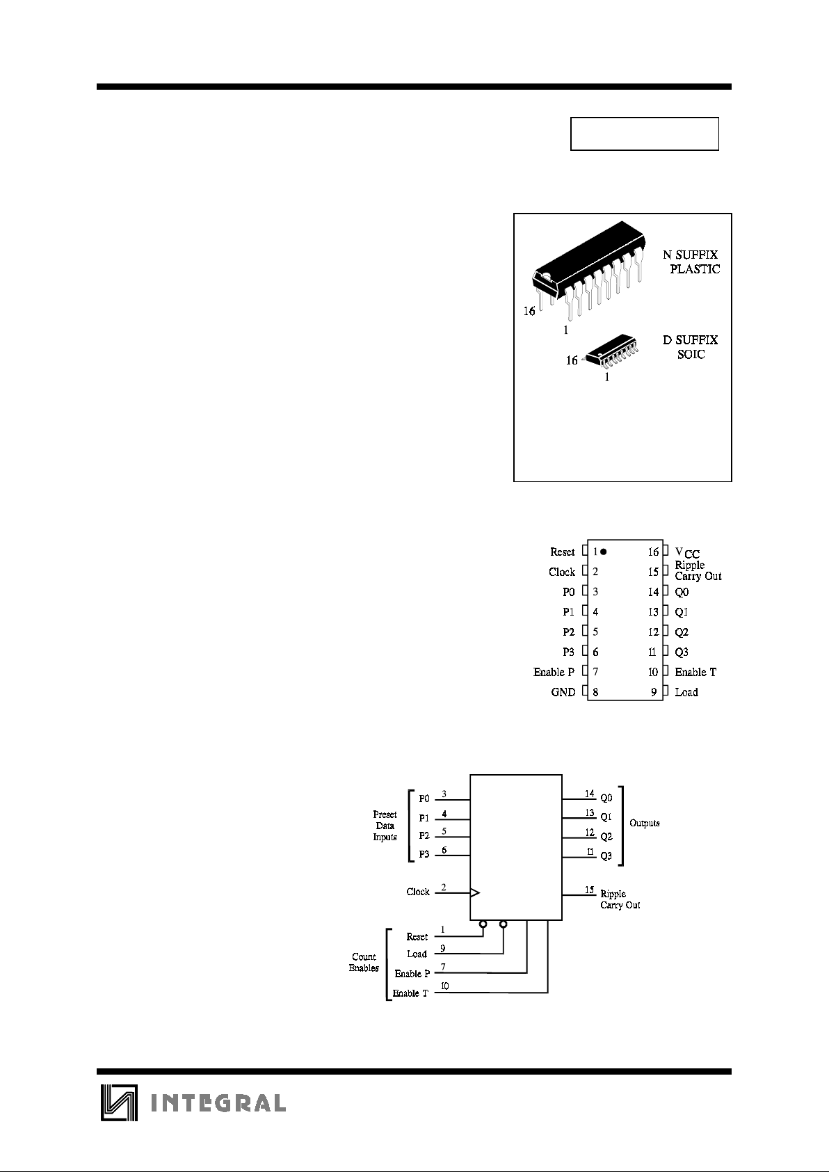
PIN ASSIGNMENT
LOGIC DIAGRAM
PIN 16 =V
CC
PIN 8 = GND
Page 2
IN74ALS161A
2
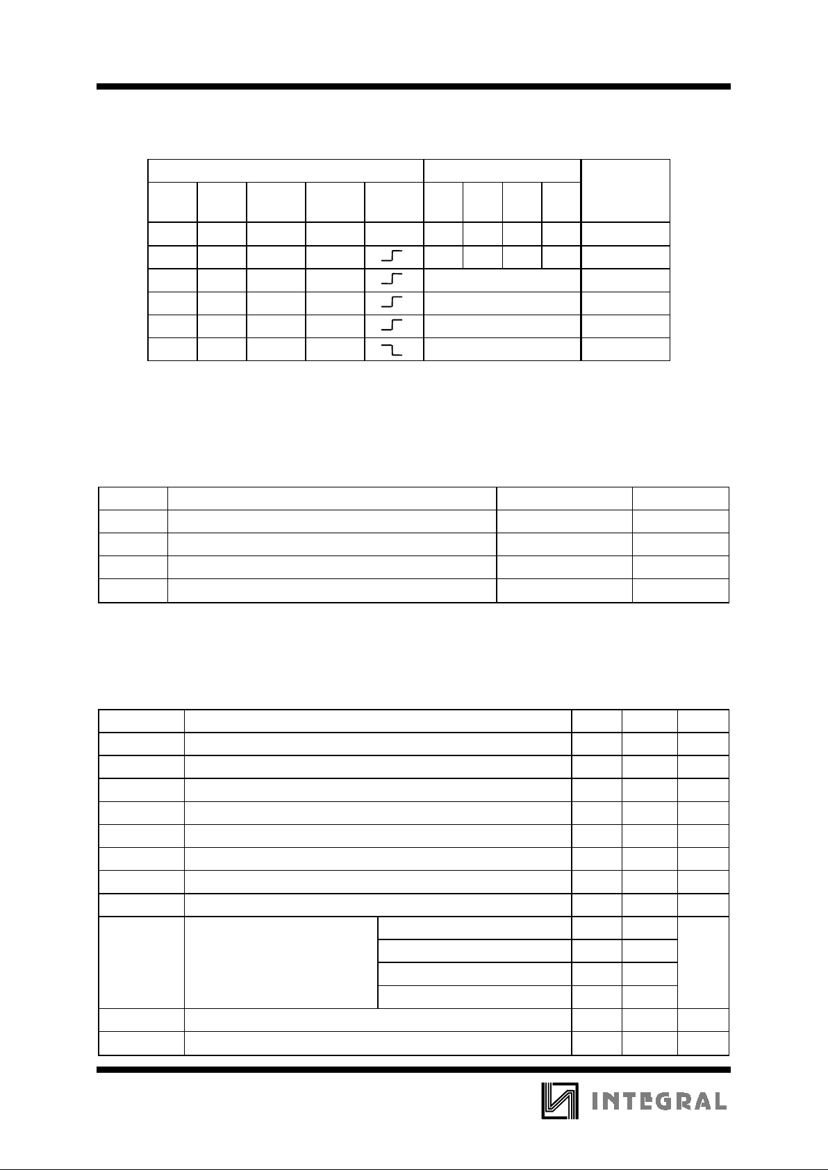
FUNCTION TABLE
Inputs Outputs
Reset Load EnablePEnableTClockQ0Q1Q2Q3 Function
L X X X X L L L L Reset to “0”
H L X X P0 P1 P2 P3 Preset Data
H H X L No change No count
H H L X No change No count
H H H H Count up Count
H X X X No change No count
X=don’t care
P0,P1,P2,P3 = logic level of Data inputs
Ripple Carry Out = Enable T • Q0 • Q1 • Q2 • Q3
MAXIMUM RATINGS
*
Symbol Parameter Value Unit
V
CC
Supply Voltage 7.0 V
V
IN
Input Voltage 7.0 V
V
OUT
Output Voltage 5.5 V
Tstg Storage Temperature Range -65 to +150
°
C
*
Maximum Ratings are those values beyond which damage to the device may occur.
Functional operation should be restricted to the Recommended Operating Conditions.
RECOMMENDED OPERATING CONDITIONS
Symbol Parameter Min Max Unit
V
CC
Supply Voltage 4.5 5.5 V
V
IH
High Level Input Voltage 2.0 V
V
IL
Low Level Input Voltage 0.8 V
I
OH
High Level Output Current -0.4 mA
I
OL
Low Level Output Current 8.0 mA
f
clock
Clock frequency 30 MHz
t
w(clock)
Width of clock pulse 25 ns
t
w(reset)
Width of reset pulse 20 ns
Data inputs P0,P1,P2,P3 20
t
su
Setup time Enable P or T 25 ns
Load 20
Reset 10
t
h
Hold time at any input 3 ns
T
A
Ambient Temperature Range -10 +70
°
C
Page 3
IN74ALS161A
3
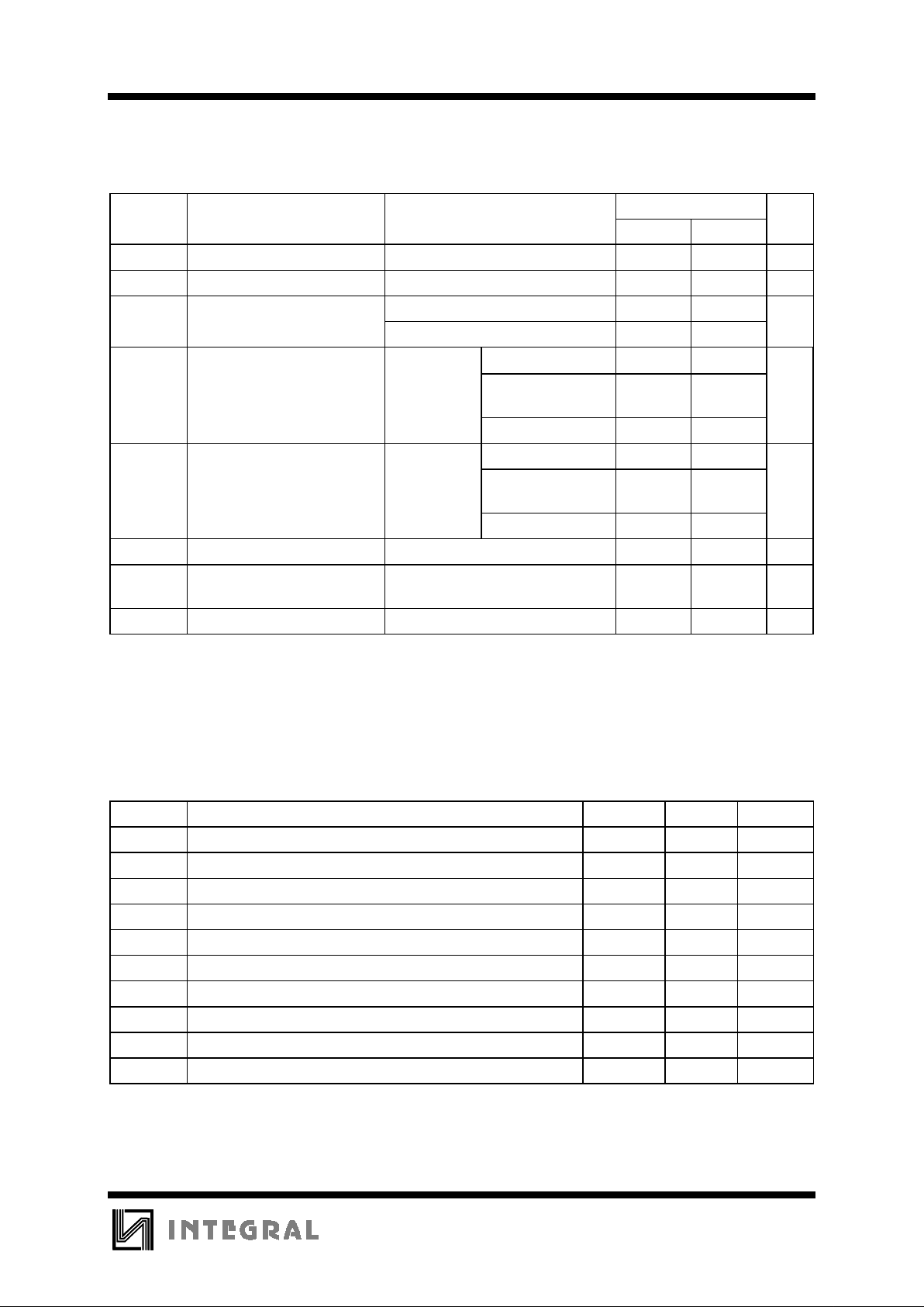
DC ELECTRICAL CHARACTERISTICS
over full operating conditions
Guaranteed Limit
Symbol Para meter Test Conditions Min Max Unit
V
IK
Input Clamp Voltage VCC = min, IIN = -18 mA -1.5 V
V
OH
High Level Output Voltage VCC = min, IOH = -0.4 mA 2.5 V
V
OL
Low Level Output Voltage VCC = min, IOL = 4 mA 0.4 V
VCC = min, IOL = 8 mA 0.5
I
IH
High Level Input Current VCC = max Data or enable P 20
µ
A
VIN =2.7 V Load, clock or
enable T
40
Reset 20
I
I
Input current at maximum VCC = max Data or enable P 0.1 mA
input voltage VIN =7.0 V Load, clock or
enable T
0.2
Reset 0.1
I
IL
Low Level Input Current VCC = max, VIN =0.4 V -0.2 mA
I
O
Output Short Circuit Current VCC = max, VO = 2.25 V
(Note 1)
-15 -112 mA
I
CC
Supply Current VCC = max 21 mA
Note 1: Not more than one output should be shorted at a time, and the duration should not exceed one second.
AC ELECTRICAL CHARACTERISTICS
(TA=25°C, VCC = 5.0 V, CL = 50 pF, RL = 500 Ω, tr tf = 2
ns)
Symbol Parameter Min Max Unit
t
PLH
Propagation Delay, Clock to Ripple carry 26 ns
t
PHL
Propagation Delay, Clock to Ripple carry 23 ns
t
PLH
Propagation Delay, Clock (load input high) to Any Q 15 ns
t
PHL
Propagation Delay, Clock (load input high) to Any Q 17 ns
t
PLH
Propagation Delay, Clock (load input low) to Any Q 15 ns
t
PHL
Propagation Delay, Clock (load input low) to Any Q 17 ns
t
PLH
Propagation Delay, Enable T to Ripple carry 13 ns
t
PHL
Propagation Delay, Enable T to Ripple carry 13 ns
t
PHL
Propagation Delay, Reset to Any Q 24 ns
t
PHL
Propagation Delay, Reset to Ripple carry 28 ns
Page 4
IN74ALS161A
4
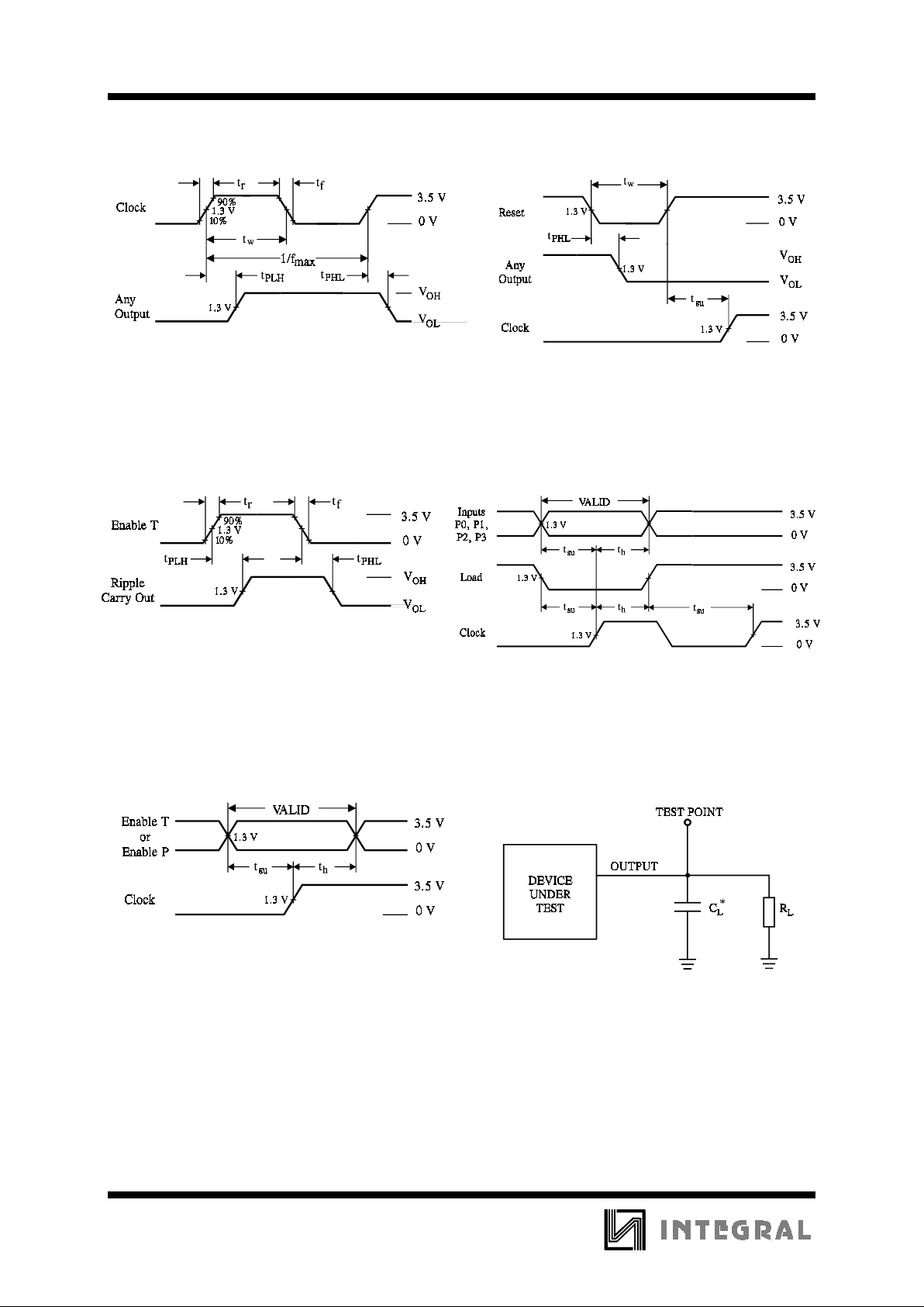
Figure 1. Switching Waveform Figure 2. Switching Waveform
Figure 3. Switching Waveform Figure 4. Switching Waveform
* Includes all probe and jig capacitance
Figure 5. Switching Waveform Figure 6. Test Circuit
Page 5
IN74ALS161A
5
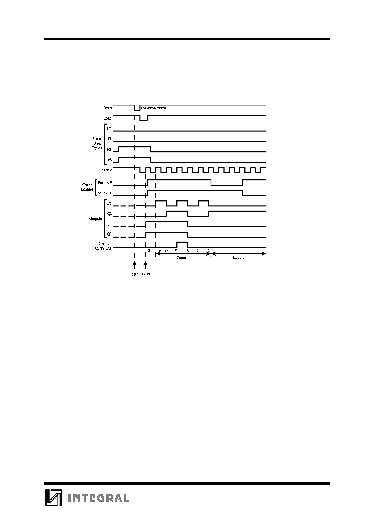
Sequence illustrated in waveforms:
1. Reset outputs to zero.
2. Preset to binary twelve.
3. Count to thirteen, fourteen, fifteen, zero, one, and two.
4. Inhibit.
Figure 7. Timing Diagram
 Loading...