

Page 1
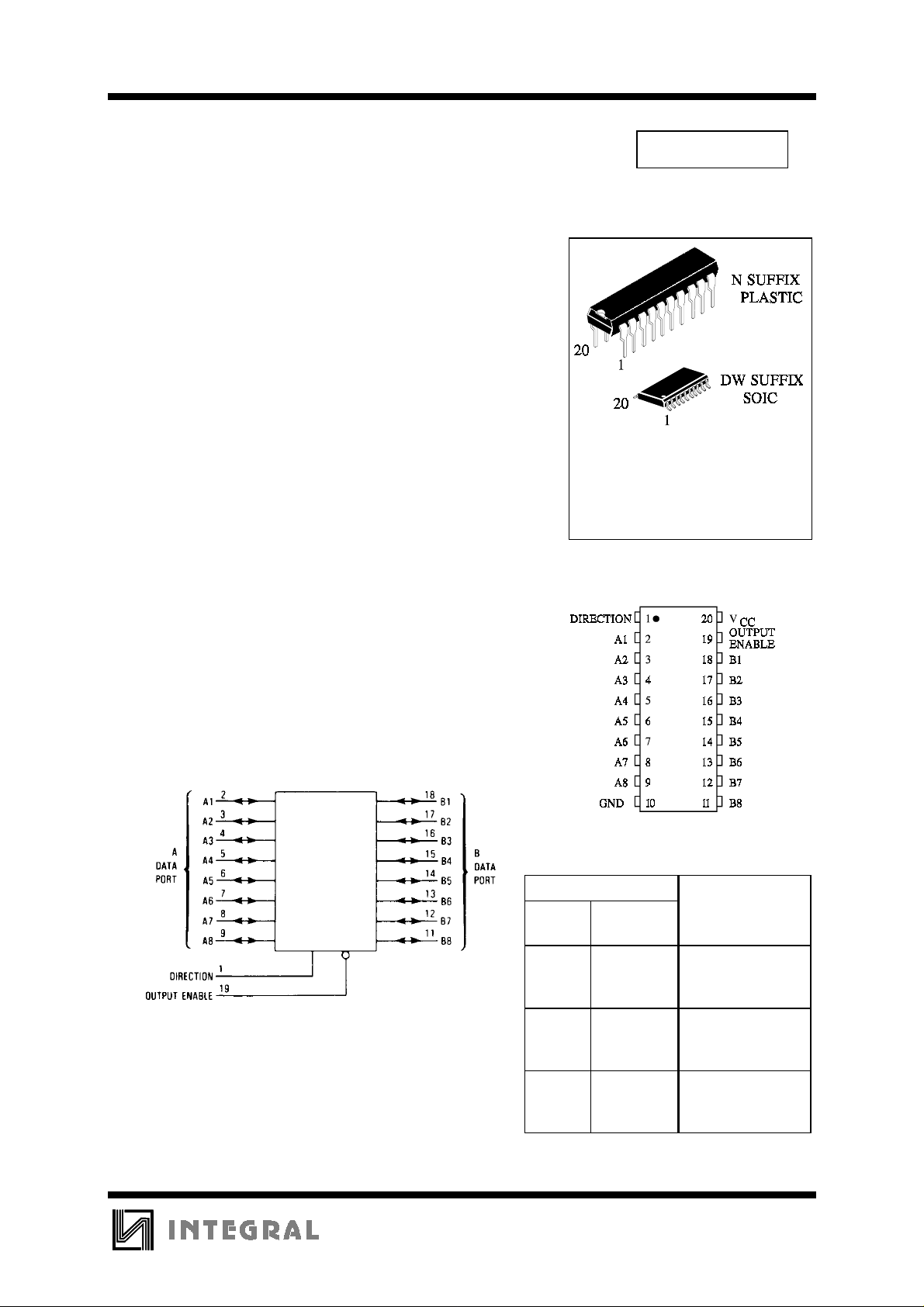
Octal 3-State Noninverting
Bus Transceiver
High-Speed Silicon-Gate CMOS
The IN74ACT245 is identical in pinout to the LS/ALS245,
HC/HCT245. The IN74ACT245 may be used as a level converter for
interfacing TTL or NMOS outputs to High Speed CMOS inputs.
The IN74ACT245 is a 3-state noninverting transceiver that is used
for 2-way asynchronous communication between data buses. The
device has an active-low Output Enable pin, which is used to place the
I/O ports into high-impedance states. The Direction control determines
whether data flows from A to B or from B to A.
•
TTL/NMOS Compatible Input Levels
•
Outputs Directly Interface to CMOS, NMOS, and TTL
•
Operating Voltage Range: 4.5 to 5.5 V
•
Low Input Current: 1.0 µA; 0.1 µA @ 25°C
•
Outputs Source/Sink 24 mA
TECHNICAL DATA
IN74ACT245
ORDERING INFORMATION
IN74ACT245N Plastic
IN74ACT245DW SOIC
TA = -40° to 85° C for all
packages
LOGIC DIAGRAM
PIN 20=V
PIN 10 = GND
CC
PIN ASSIGNMENT
FUNCTION TABLE
Control Inputs
Output
Enable
L L Data Transmitted
L H Data Transmitted
H X Buses Isolated
X = don’t care
Direction Operation
from Bus B to
Bus A
from Bus A to
Bus B
(High Impedanc e
State)
331
Page 2
IN74ACT245
MAXIMUM RATINGS
*
Symbol Parameter Value Unit
V
CC
V
V
OUT
I
IN
I
OUT
I
CC
P
DC Supply Voltage (Referenced to GND) -0.5 to +7.0 V
DC Input Voltage (Referenced to GND) -0.5 to VCC +0.5 V
IN
DC Output Voltage (Referenced to GND) -0.5 to VCC +0.5 V
DC Input Current, per Pin
DC Output Sink/Source Current, per Pin
DC Supply Current, VCC and GND Pins
Power Dissipation in Still Air, Plastic DIP+
D
SOIC Package+
±
20
±
50
±
50
750
500
Tstg Storage Temperature -65 to +150
T
Lead Temperature, 1 mm from Case for 10 Seconds
L
260
(Plastic DIP or SOIC Package)
*
Maximum Ratings are those values beyond which damage to the device may occur.
Functional operation should be restricted to the Recommended Operating Conditions.
+Derating - Plastic DIP: - 10 mW/°C from 65° to 125°C
SOIC Package: : - 7 mW/°C from 65° to 125°C
mA
mA
mA
mW
°
C
°
C
RECOMMENDED OPERATING CONDITIONS
Symbol Parameter Min Max Unit
V
CC
VIN, V
T
J
T
A
I
OH
I
OL
tr, t
f
*
VIN from 0.8 V to 2.0 V
This device c ontains p rote ction ci rcuitr y to guard a gainst damage d ue to high st atic voltages or electr ic
fields. However, precautions must be taken to avoid applications of any voltage higher than maximum rated
voltages to this high-impedance circuit. For proper operation, V
GND≤(V
Unused inputs must always be tied to an appropriate logic voltage level (e.g., either GND or V
Unused outputs must be left open.
DC Supply Voltage (Referenced to GND) 4.5 5.5 V
DC Input Voltage, Output Voltage (Referenced to GND) 0 V
OUT
Junction Temperature (PDIP) 140
Operating Temperature, All Package Types -40 +85
Output Current - High -24 mA
Output Current - Low 24 mA
Input Rise and Fall Time
(except Schmitt Inputs)
IN
or V
OUT
)≤VCC.
*
V
V
=4.5 V
CC
=5.5 V
CC
and V
IN
0
0
should be constrained to the range
OUT
10
8.0
CC
V
°
C
°
C
ns/V
CC
).
332
Page 3
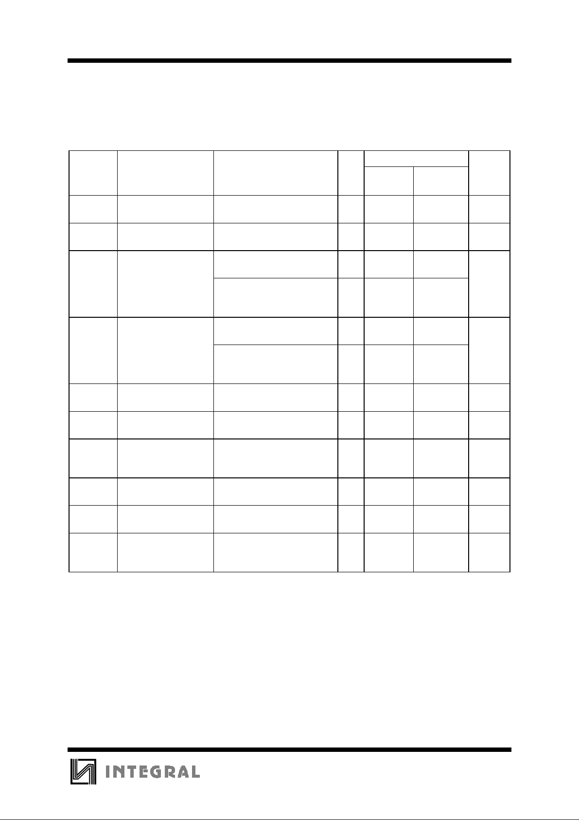
IN74ACT245
DC ELECTRICAL CHARACTERISTICS
(Voltages Referenced to GND)
Symbol Parameter Test Conditions V
V
Minimum High-Level
IH
V
=0.1 V or VCC-0.1 V 4 .5
OUT
Input Voltage
V
Maximum Low -
IL
V
=0.1 V or VCC-0.1 V 4 .5
OUT
Level Input Voltage
V
OH
Minimum High-Level
I
OUT
≤ -50 µA
Output Voltage
*
VIN=VIH or V
IL
IOH=-24 mA
I
=-24 mA
OH
V
OL
Maximum Low-Level
I
OUT
≤ 50 µA
Output Voltage
*
VIN=VIH or V
IL
IOL=24 mA
I
=24 mA
OL
I
IN
Maximum Input
VIN=VCC or GND 5.5
Leakage Current
∆
I
CCT
I
OZ
Additional Max.
I
/Input
CC
Maximum ThreeState Leakage
Current
I
OLD
+Minimum Dynamic
V
IN=VCC
V
IN
V
IN =VCC
V
OUT =VCC
V
OLD
- 2.1 V 5.5 1.5 mA
(OE)= VIH or V
IL
or GND
or GND
=1.65 V Max 5.5 75 mA
Output Current
I
OHD
+Minimum Dynamic
V
=3.85 V Min 5.5 -75 mA
OHD
Output Current
I
CC
Maximum Quiescent
VIN=VCC or GND 5.5 8.0 80
Supply Current
(per Package)
*
All outputs loaded; thresholds on input associated with output under test.
+Maximum test duration 2.0 ms, one output loaded at a time.
V
5.5
5.5
4.5
5.5
4.5
5.5
4.5
5.5
4.5
5.5
5.5
CC
Guaranteed Limits
25 °C-40
2.0
2.0
0.8
0.8
4.4
5.4
3.86
4.86
0.1
0.1
0.36
0.36
±
0.1
±
0.6
°
C to
85°C
2.0
2.0
0.8
0.8
4.4
5.4
3.76
4.76
0.1
0.1
0.44
0.44
±
1.0
±
6.0
Unit
V
V
V
V
µ
A
µ
A
µ
A
333
Page 4
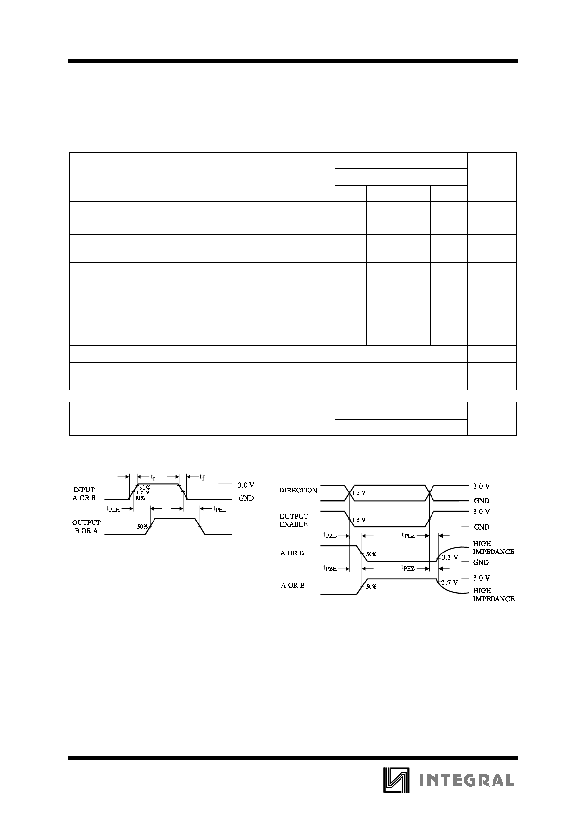
IN74ACT245
AC ELECTRICAL CHARACTERISTICS
Symbol Parameter
t
PLH
t
PHL
t
PZH
t
PZL
t
PHZ
t
PLZ
C
IN
C
OUT
C
PD
Propagation Delay, A to B, B to A (Figure 1) 1.5 7.5 1.5 8.0 ns
Propagation Delay, A to B, B to A (Figure 1) 1.5 8.0 1.0 9.0 ns
Propagation Delay, Direction or Output Enable to A
or B (Figure 2)
Propagation Delay, Direction or Output Enable to A
or B (Figure 2)
Propagation Delay, Direction or Output Enable to A
or B (Figure 2)
Propagation Delay, Direction or Output Enable to A
or B (Figure 2)
Maximum Input Capacitance 4.5 4.5 pF
Maximum Three-State I/O Capacitance
(I/O in High-Impedance State)
Power Dissipation Capacitance 45 pF
(VCC=5.0 V ± 10%, CL=50pF, Input tr=tf=3.0 ns)
Guaranteed Limits
25 °C-40
°
C to 85°C
Min Max Min Max
1.5 10.0 1.5 11.0 ns
1.5 10.0 1.5 12.0 ns
1.5 10.0 1.0 11.0 ns
2.0 10.0 1.5 11.0 ns
15 15 pF
Typical @25°C,VCC=5.0 V
Unit
334
Figure 1. Switching Waveforms Figure 2. Switching Waveforms
Page 5

EXPANDED LOGIC DIAGRAM
IN74ACT245
335
 Loading...