

Page 1
TECHNICAL DATA
Quad 2-Input Data Selector/Multiplexer
High-Speed Silicon-Gate CMOS
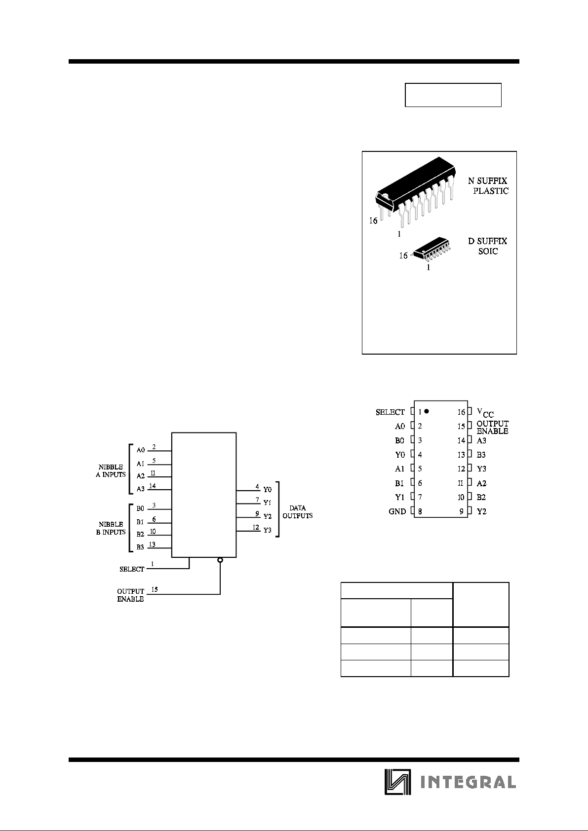
The IN74ACT157 is identical in pinout to the LS/ALS157,
HC/HCT157. The IN74ACT157 may be used as a level converter for
interfacing TTL or NMOS outputs to High Speed CMOS inputs.
This device routes 2 nibbles (A or B) to a single port (Y) as
determined by the Select input. The data is presented at the outputs in
noninvertered form. A high level on the Outp ut Enable input sets all
four Y outputs to a low level.
•
TTL/NMOS Compatible Input Levels
•
Outputs Directly Interface to CMOS, NMOS, and TTL
•
Operating Voltage Range: 4.5 to 5.5 V
•
Low Input Current: 1.0 µA; 0.1 µA @ 25°C
•
Outputs Source/Sink 24 mA
IN74ACT157
ORDERING INFORMATION
IN74ACT157N Plastic
IN74ACT157D SOIC
TA = -40° to 85° C for all
packages
LOGIC DIAGRAM
PIN 16 =V
PIN 8 = GND
CC
PIN ASSIGNMENT
FUNCTION TABLE
Inputs Outputs
Output
Enable
HXL
LLA0-A3
LHB0-B3
X=don’t care
A0-A3,B0-B3=the levels of the respective
Data-Word Inputs
Select Y0-Y3
198
Page 2
IN74ACT157
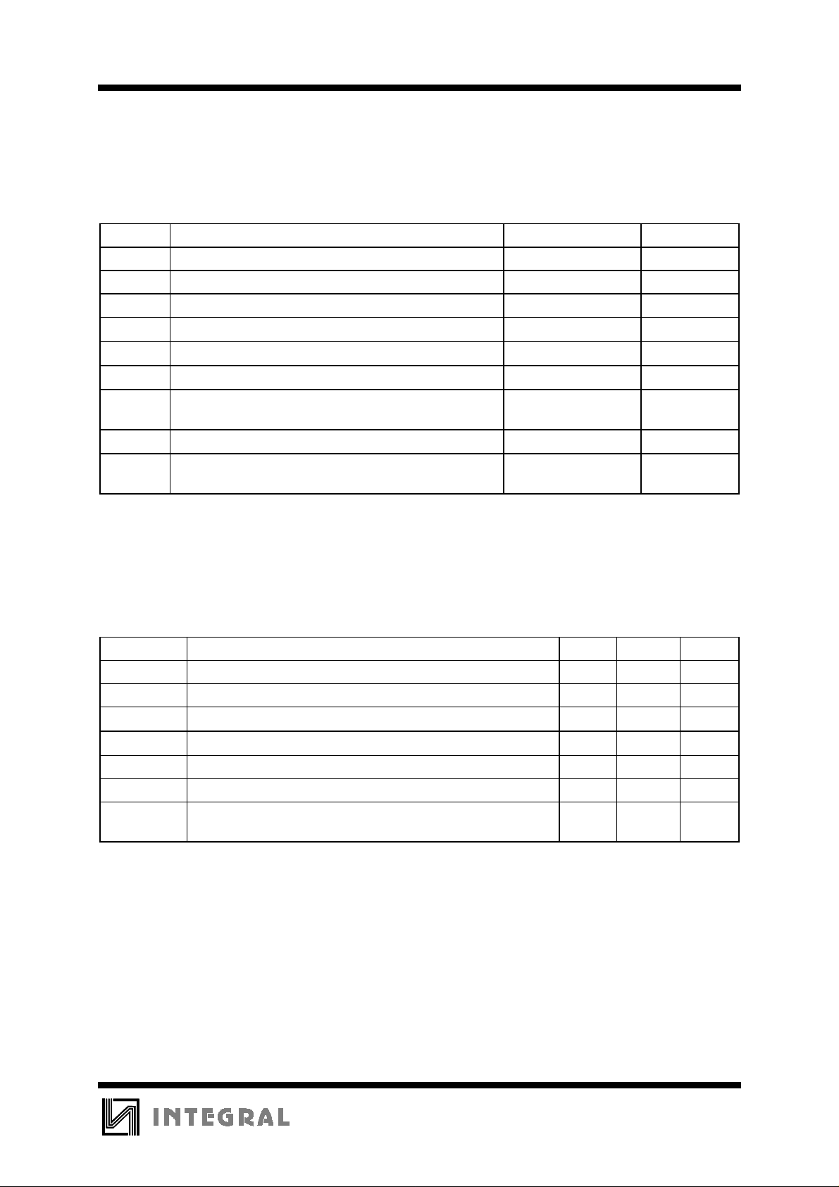
MAXIMUM RATINGS
*
Symbol Parameter Value Unit
V
CC
V
V
OUT
I
IN
I
OUT
I
CC
P
DC Supply Voltage (Referenced to GND) -0.5 to +7.0 V
DC Input Voltage (Referenced to GND) -0.5 to VCC +0.5 V
IN
DC Output Voltage (Referenced to GND) -0.5 to VCC +0.5 V
DC Input Current, per Pin
DC Output Sink/Source Current, per Pin
DC Supply Current, VCC and GND Pins
Power Dissipation in Still Air, Plastic DIP+
D
SOIC Package+
±
20
±
50
±
50
750
500
Tstg Storage Temperature -65 to +150
T
Lead Temperature, 1 mm from Case for 10 Seconds
L
260
(Plastic DIP or SOIC Package)
*
Maximum Ratings are those values beyond which damage to the device may occur.
Functional operation should be restricted to the Recommended Operating Conditions.
+Derating - Plastic DIP: - 10 mW/°C from 65° to 125°C
SOIC Package: : - 7 mW/°C from 65° to 125°C
mA
mA
mA
mW
°
C
°
C
RECOMMENDED OPERATING CONDITIONS
Symbol Parameter Min Max Unit
V
CC
VIN, V
T
J
T
A
I
OH
I
OL
tr, t
f
*
VIN from 0.8 V to 2.0 V
This device c ontains p rote ction ci rcuitr y to guard a gainst damage d ue to high st atic voltages or electr ic
fields. However, precautions must be taken to avoid applications of any voltage higher than maximum rated
voltages to this high-impedance circuit. For proper operation, V
GND≤(V
Unused inputs must always be tied to an appropriate logic voltage level (e.g., either GND or V
Unused outputs must be left open.
DC Supply Voltage (Referenced to GND) 4.5 5.5 V
DC Input Voltage, Output Voltage (Referenced to GND) 0 V
OUT
Junction Temperature (PDIP) 140
Operating Temperature, All Package Types -40 +85
Output Current - High -24 mA
Output Current - Low 24 mA
Input Rise and Fall Time
(except Schmitt Inputs)
IN
or V
OUT
)≤VCC.
*
V
V
=4.5 V
CC
=5.5 V
CC
and V
IN
0
0
should be constrained to the range
OUT
10
8.0
CC
V
°
C
°
C
ns/V
CC
).
199
Page 3
IN74ACT157
DC ELECTRICAL CHARACTERISTICS
(Voltages Referenced to GND)
Symbol Parameter Test Conditions V
V
Minimum High-Level
IH
V
=0.1 V or VCC-0.1 V 4 .5
OUT
Input Voltage
V
Maximum Low -
IL
V
=0.1 V or VCC-0.1 V 4 .5
OUT
Level Input Voltage
V
OH
Minimum High-Level
I
OUT
≤ -50 µA
Output Voltage
*
VIN=VIH or V
IL
IOH=-24 mA
I
=-24 mA
OH
V
OL
Maximum Low-Level
I
OUT
≤ 50 µA
Output Voltage
*
VIN=VIL or V
IH
IOL=24 mA
I
=24 mA
OL
I
IN
Maximum Input
VIN=VCC or GND 5.5
Leakage Current
∆
I
CCT
I
OLD
Additional Max
I
/Input
CC
+Minimum Dynamic
V
IN=VCC
V
OLD
- 2.1 V 5.5 1.5 mA
=1.65 V Max 5.5 75 mA
Output Current
I
OHD
+Minimum Dynamic
V
=3.85 V Min 5.5 -75 mA
OHD
Output Current
I
CC
Maximum Quiescent
VIN=VCC or GND 5.5 8.0 80
Supply Current
(per Package)
*
All outputs loaded; thresholds on input associated with output under test.
+Maximum test duration 2.0 ms, one output loaded at a time.
V
5.5
5.5
4.5
5.5
4.5
5.5
4.5
5.5
4.5
5.5
CC
Guaranteed Limits
25 °C-40
2.0
2.0
0.8
0.8
4.4
5.4
3.86
4.86
0.1
0.1
0.36
0.36
±
0.1
°
C to
85°C
2.0
2.0
0.8
0.8
4.4
5.4
3.76
4.76
0.1
0.1
0.44
0.44
±
1.0
Unit
V
V
V
V
µ
A
µ
A
200
Page 4
IN74ACT157
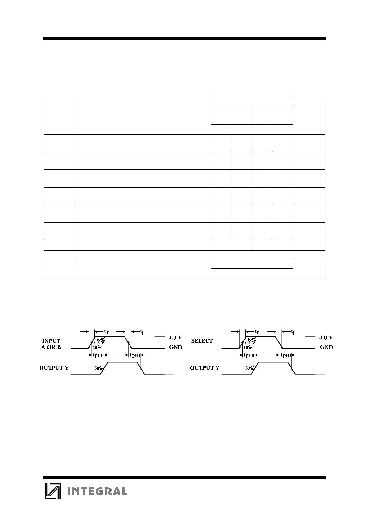
AC ELECTRICAL CHARACTERISTICS
Symbol Parameter
t
t
t
t
t
t
C
C
PLH
PHL
PLH
PHL
PLH
PHL
IN
PD
Propagation Delay, Select to Output Y
(Figure 2)
Propagation Delay, Select to Output Y
(Figure 2)
Propagation Delay, Output Enable to
Output Y (Figure 3)
Propagation Delay, Output Enable to
Output Y (Figure 3)
Propagation Delay, Input A or B to Output Y
(Figure 1)
Propagation Delay, Input A or B to Output Y
(Figure 1)
Maximum Input Capacitance 4.5 4.5 pF
Power Dissipation Capacitance 50 pF
(VCC=5.0 V ± 10%, CL=50pF,Input tr=tf=3.0 ns)
Guaranteed Limits
25 °C-40
°
C to
85°C
Min Max Min Max
2.0 9.0 1.5 10.0 ns
2.0 9.5 2.0 10.5 ns
1.5 10 1.5 11.5 ns
1.5 8.5 1.0 9.0 ns
1.5 7.0 1.0 8.5 ns
1.5 7.5 1.0 8.5 ns
Typical @25°C,VCC=5.0 V
Unit
Figure 1. Switching Waveforms Figure 2. Switching Waveforms
201
Page 5
IN74ACT157
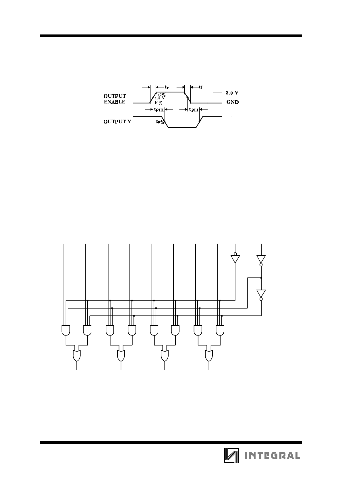
Figure 3. Switching Waveforms
EXPANDED LOGIC DIAGRAM
A0 B0 A1 B1 A2 B2 A3 B3 OE SELECT
Y0 Y1 Y2 Y3
202
 Loading...