

Page 1
TECHNICAL DATA
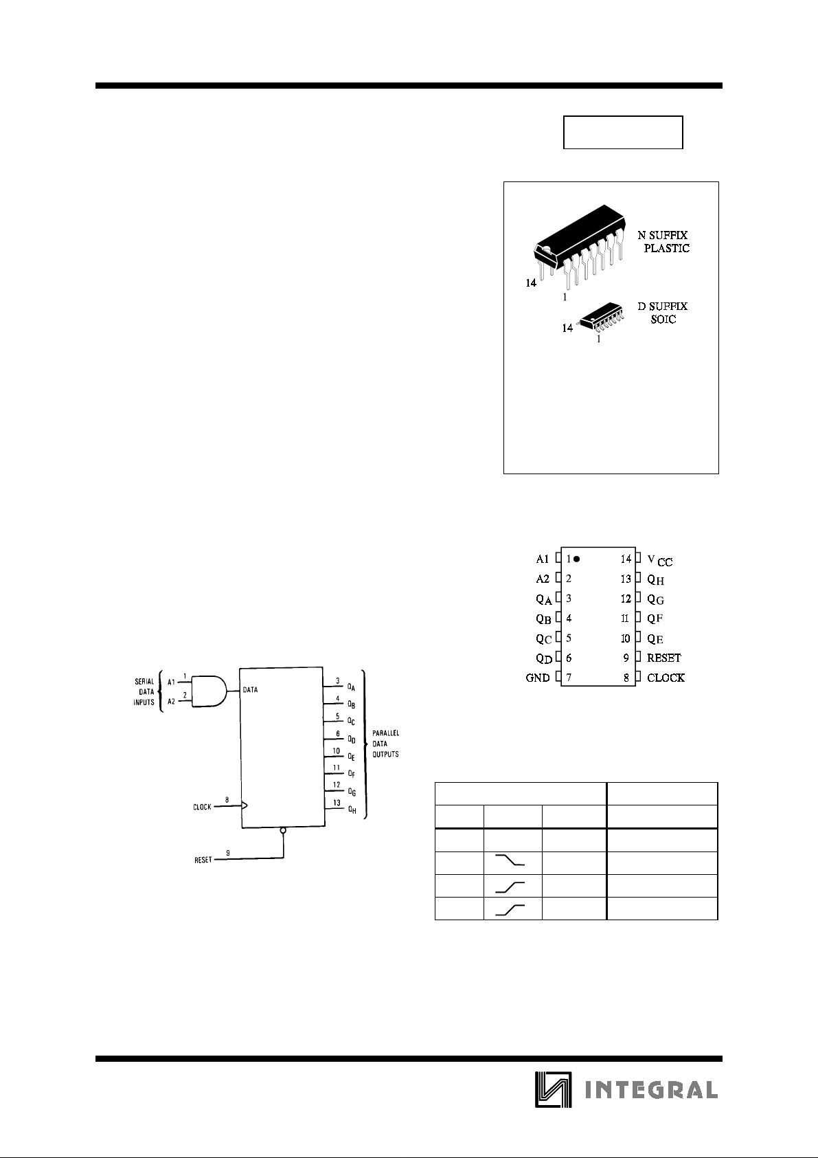
8-Bit Serial-Input/Parallel-Output
Shift register
High-Speed Silicon-Gate CMOS
The IN74AC164 is identical in pinout to the LS/ALS164,
HC/HCT164. The device inputs are compatible with standard CMOS
outputs; with pullup resistors, they are compatible with LS/ALS
outputs.
The IN74AC164 is an 8-bit, serial-input to parallel-output shift
register. Two serial data inputs, A1 and A2, are provided so that one
input may be used as a data enable. Data is entered on each rising edge
of the clock. The active-low asynchronous Reset overrides the Clock
and Serial Data inputs.
•
Outputs Directly Interface to CMOS, NMOS, and TTL
•
Operating Voltage Range: 2.0 to 6.0 V
•
Low Input Current: 1.0 µA; 0.1 µA @ 25°C
•
High Noise Immunity Characteristic of CMOS Devices
•
Outputs Source/Sink 24 mA
IN74AC164
ORDERING INFORMATION
IN74AC164N Plastic
IN74AC164D SOIC
TA = -40° to 85° C for all
packages
PIN ASSIGNMENT
LOGIC DIAGRAM
PIN 14 =V
PIN 7 = GND
CC
FUNCTION TABLE
Inputs Outputs
Reset Clock A1 A2 QA QB ... Q
L X X X L L ... L
H X X no change
H H D D QAn ... Q
H D H D QAn ... Q
D = data input
X = don’t care
Q
- Q
An
rising edge at the clock input.
= data shifted from the previous stage on a
Gn
H
Gn
Gn
244
Page 2
IN74AC164
MAXIMUM RATINGS
*
Symbol Parameter Value Unit
V
CC
V
V
OUT
I
IN
I
OUT
I
CC
P
DC Supply Voltage (Referenced to GND) -0.5 to +7.0 V
DC Input Voltage (Referenced to GND) -0.5 to VCC +0.5 V
IN
DC Output Voltage (Referenced to GND) -0.5 to VCC +0.5 V
DC Input Current, per Pin
DC Output Sink/Source Current, per Pin
DC Supply Current, VCC and GND Pins
Power Dissipation in Still Air, Plastic DIP+
D
SOIC Package+
±
20
±
50
±
50
750
500
Tstg Storage Temperature -65 to +150
T
Lead Temperature, 1 mm from Case for 10 Seconds
L
260
(Plastic DIP or SOIC Package)
*
Maximum Ratings are those values beyond which damage to the device may occur.
Functional operation should be restricted to the Recommended Operating Conditions.
+Derating - Plastic DIP: - 10 mW/°C from 65° to 125°C
SOIC Package: : - 7 mW/°C from 65° to 125°C
mA
mA
mA
mW
°
C
°
C
RECOMMENDED OPERATING CONDITIONS
Symbol Parameter Min Max Unit
V
CC
VIN, V
T
J
T
A
I
OH
I
OL
tr, t
f
*
VIN from 30% to 70% V
This device c ontains p rote ction ci rcuitr y to guard a gainst damage d ue to high st atic voltages or electr ic
fields. However, precautions must be taken to avoid applications of any voltage higher than maximum rated
voltages to this high-impedance circuit. For proper operation, V
GND≤(V
Unused inputs must always be tied to an appropriate logic voltage level (e.g., either GND or V
Unused outputs must be left open.
DC Supply Voltage (Referenced to GND) 2.0 6.0 V
DC Input Voltage, Output Voltage (Referenced to GND) 0 V
OUT
Junction Temperature (PDIP) 140
Operating Temperature, All Package Types -40 +85
Output Current - High -24 mA
Output Current - Low 24 mA
Input Rise and Fall Time
(except Schmitt Inputs)
IN
or V
OUT
)≤VCC.
CC
*
V
V
V
=3.0 V
CC
=4.5 V
CC
=5.5 V
CC
and V
IN
0
0
0
should be constrained to the range
OUT
CC
150
40
25
V
°
C
°
C
ns/V
CC
).
245
Page 3

IN74AC164
DC ELECTRICAL CHARACTERISTICS
(Voltages Referenced to GND)
Symbol Parameter Test Conditions V
V
Minimum High-Level
IH
V
=0.1 V or VCC-0.1 V 3 .0
OUT
Input Voltage
V
Maximum Low -
IL
V
=0.1 V or VCC-0.1 V 3 .0
OUT
Level Input Voltage
V
OH
Minimum High-Level
I
OUT
≤ -50 µA
Output Voltage
*
VIN=VIH or V
IL
IOH=-12 mA
I
=-24 mA
OH
I
=-24 mA
OH
V
OL
Maximum Low-Level
I
OUT
≤ 50 µA
Output Voltage
*
VIN=VIH or V
IL
IOL=12 mA
I
=24 mA
OL
I
=24 mA
OL
I
IN
Maximum Input
VIN=VCC or GND 5.5
Leakage Current
I
OLD
+Minimum Dynamic
V
=1.65 V Max 5.5 75 mA
OLD
Output Current
I
OHD
+Minimum Dynamic
V
=3.85 V Min 5.5 -75 mA
OHD
Output Current
I
CC
Maximum Quiescent
VIN=VCC or GND 5.5 4.0 40
Supply Current
(per Package)
*
All outputs loaded; thresholds on input associated with output under test.
+Maximum test duration 2.0 ms, one output loaded at a time.
Note: I
IN
and I
@ 3.0 V are guaranteed to be less than or equal to the respective limit @ 5.5 V V
CC
V
4.5
5.5
4.5
5.5
3.0
4.5
5.5
3.0
4.5
5.5
3.0
4.5
5.5
3.0
4.5
5.5
CC
Guaranteed Limits
25 °C-40
2.1
3.15
3.85
0.9
1.35
1.65
2.9
4.4
5.4
2.56
3.86
4.86
0.1
0.1
0.1
0.36
0.36
0.36
±
0.1
°
C to
85°C
2.1
3.15
3.85
0.9
1.35
1.65
2.9
4.4
5.4
2.46
3.76
4.76
0.1
0.1
0.1
0.44
0.44
0.44
±
1.0
CC
Unit
V
V
V
V
µ
A
µ
A
246
Page 4

IN74AC164
AC ELECTRICAL CHARACTERISTICS
(CL=50pF,Input tr=tf=3.0 ns)
Symbol Parameter V
f
max
t
PLH
t
PHL
t
PHL
C
IN
C
PD
*
Voltage Range 3.3 V is 3.3 V ±0.3 V
Maximum Clock Frequency (Figur e 1) 3.3
Propagat ion Delay, Clock to Q (Figure 1) 3.3
Propagat ion Delay, Clock to Q (Figure 1) 3.3
Propagation Delay, Reset to Q (Figure 2) 3.3
Maximum Input Capacitance 5.0 4.5 4.5 pF
Power Dissipation Capacitance 35 pF
Voltage Range 5.0 V is 5.0 V ±0.5 V
*
V
CC
Guaranteed Limits
25 °C-40
Min Max Min Max
125
5.0
5.0
5.0
5.0
150
4.0
2.5
3.0
2.0
3.0
2.0
13.5
10.0
14.0
10.0
12.0
9.5
Typical @25°C,VCC=5.0 V
100
125
3.5
2.0
3.0
1.5
3.0
2.0
°
C to
85°C
16.0
10.5
14.5
10.5
13.5
10.5
Unit
MHz
ns
ns
ns
TIMING REQUIREMENTS
(CL=50pF, Input tr=tf=3.0 ns)
Symbol Parameter V
t
su
Minimum Set up Time, A1 or A2 to Clock
(Figure 3)
t
h
Minimum Hold Time, C lock to A1 or A2
(Figure 3)
t
w
Minimum Pulse Width, Clock or Reset
(Figures 1,2)
t
rec
Minimum Rec overy Time, Reset to Clock
(Figure 2)
*
Voltage Range 3.3 V is 3.3 V ±0.3 V
Voltage Range 5.0 V is 5.0 V ±0.5 V
V
CC
3.3
5.0
3.3
5.0
3.3
5.0
3.3
5.0
*
Guaranteed Limits
25 °C-40
°
C to
Unit
85°C
6.5
4.5
0
0.5
4.0
3.5
0
0
7.5
5.0
0
0.5
4.5
3.5
0
0
ns
ns
ns
ns
247
Page 5

IN74AC164
Figure 1. Switching Waveforms Figure 2. Switching Waveforms
Figure 3. Switching Waveforms
TIMING DIAGRAM
EXPANDED LOGIC DIAGRAM
248
 Loading...