

Datasheet IMP812REUS-T, IMP812MEUS-T, IMP812LEUS-T, IMP812JEUS-T, IMP811TEUS-T Datasheet (IMP)
...Page 1
©
1999 IMP, Inc. 408-432-9100/www.impweb.com 1
Key Features
Applications
4-Pin
4-Pin µµ
P V
P V
olt
olt
ag
ag
e Super
e Super
visor
visor
wit
wit
h Manual R
h Manual R
eset
eset
◆ Computers and controllers
◆ Embedded controllers
◆ Battery operated systems
◆ Intelligent instruments
◆ Wireless communication systems
◆ PDAs and handheld equipment
◆
Improved Maxim MAX811/MAX812 replacement
—
Specified to 105°C
—
New 4.0V threshold option
◆
6µA supply current
◆
Monitor 5V, 3.3V and 3V supplies
◆
Manual reset input
◆
140ms min. reset pulse width
◆
Guaranteed over temperature
◆
Active-LOW reset valid with 1.1V supply
(IMP811)
◆
Small 4-pin SOT-143 package
◆
No external components
◆
Power-supply transient-immune design
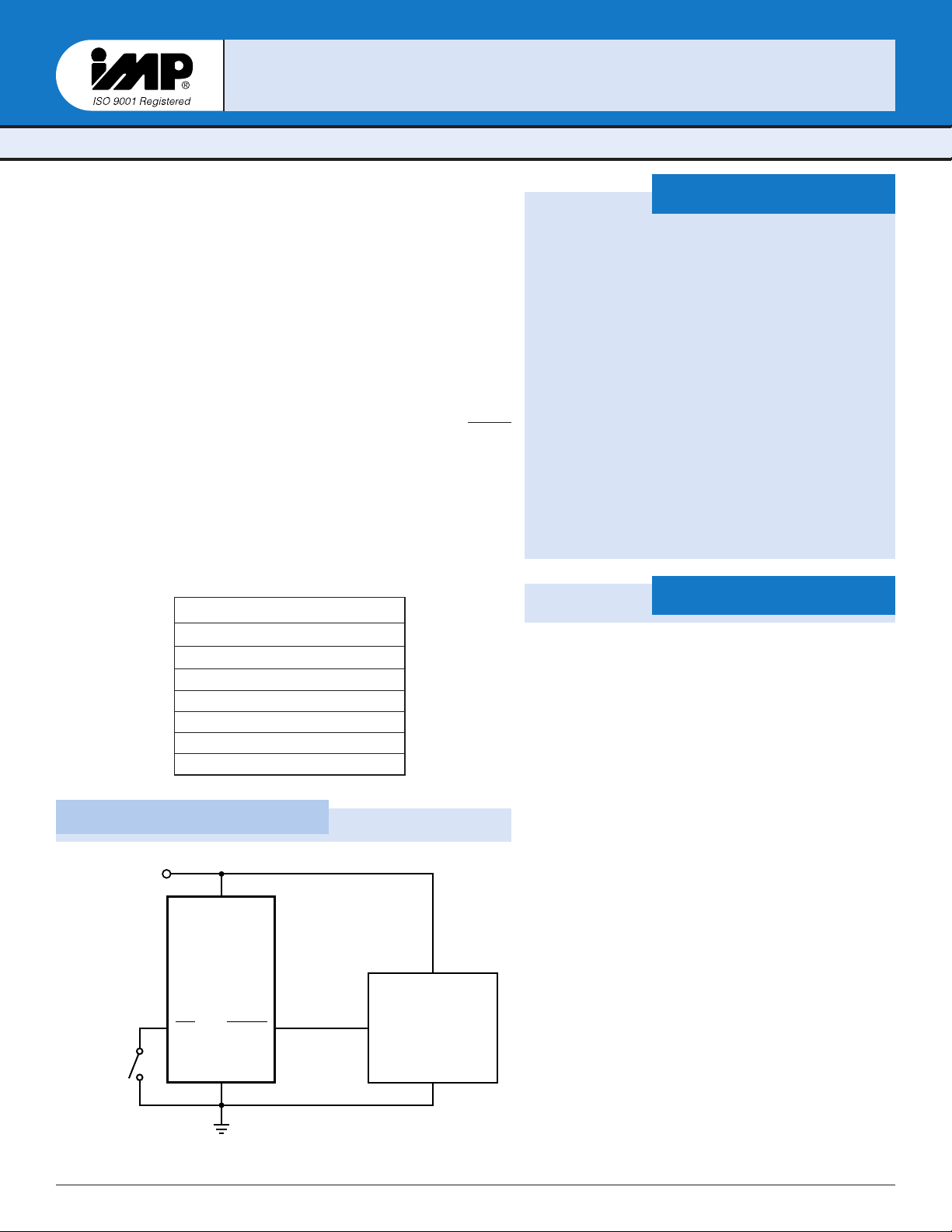
Block Diagrams
IMP811
(IMP812)
V
CC
V
CC
V
CC
GND GND
RESET
(RESET)
Manual
Reset
MR
811/12_01.eps
µC or µP
RESET
Input
The IMP811/IMP812 are low-power supervisors designed to monitor
voltage levels of 3.0V, 3.3V and 5.0V power supplies in low-power
microprocessor (µP), microcontroller (µC) and digital systems. Each features a debounced manual reset input. The IMP811/812 are improved
drop-in replacements for the Maxim MAX811/812 with extended
temperature specifications to 105°C.
A reset signal is issued if the power supply voltage drops below a preset
threshold and is asserted for at least 140ms after the supply has risen
above the reset threshold. The IMP811 has an active-low output RESET
that is guaranteed to be in the correct state for V
CC
down to 1.1V. The
IMP812 has an active-high output RESET. The reset comparator is
designed to ignore fast transients on V
CC
.
Low power consumption makes the IMP811/IMP812 ideal for use in
portable and battery-operated equipment. Available in a compact 4-pin
SOT143 package, the devices use minimal board space.
Six voltage thresholds are available to support 3V to 5V systems:
IMP8
IMP81111
, IMP8
, IMP81122
POWER MANAGEMENT
Reset Threshold
Suffix Voltage (V)
L 4.63
M 4.38
J 4.00
T 3.08
S 2.93
R 2.63
Page 2
IMP8
IMP81111
, IMP8
, IMP81122
2
408-432-9100/www.impweb.com
©
1999 IMP, Inc.
Ordering Information
Pin Configuration
IMP811
(IMP812)
GND
(RESET) RESET
V
CC
4
MR
3
2
1
811/12_02.eps
SOT143
Package Marking
2
Part Number
1
Reset Threshold (V) Temperature Range Pin-Package
(XX Lot Code)
IMP811 Active LOW Reset with Active LOW Manual Reset
IMP811LEUS-T 4.63 –40°C to +105°C 4-SOT143 AMXX
IMP811MEUS-T 4.38 –40°C to +105°C 4-SOT143 ANXX
IMP811JEUS-T 4.00 – 40°C to +105°C 4-SOT143 AOXX
IMP811TEUS-T 3.08 –40°C to +105°C 4-SOT143 APXX
IMP811SEUS-T 2.93 –40°C to +105°C 4-SOT143 AQXX
IMP811REUS-T 2.63 –40°C to +105°C 4-SOT143 ARXX
IMP812 Active HIGH Reset with Active LOW Manual Reset
IMP812LEUS-T 4.63 –40°C to +105°C 4-SOT143 ASXX
IMP812MEUS-T 4.38 –40°C to +105°C 4-SOT143 ATXX
IMP812JEUS-T 4.00 – 40°C to +105°C 4-SOT143 AUXX
IMP812TEUS-T 3.08 – 40°C to +105°C 4-SOT143 AVXX
IMP812SEUS-T 2.93 –40°C to +105°C 4-SOT143 AWXX
IMP812REUS-T 2.63 –40°C to +105°C 4-SOT143 AXXX
Pin Terminal Voltage with Respect to Ground
V
CC
. . . . . . . . . . . . . . . . . . . . . . . . . . . . . . . . . –0.3V to 6.0V
RESET, RESET and MR . . . . . . . . . . . . . . . . . –0.3V to (V
CC
+ 0.3V)
Input Current at V
CC
and MR . . . . . . . . . . . 20mA
Output Current: RESET or RESET . . . . . . . 20mA
Rate of Rise at V
CC
. . . . . . . . . . . . . . . . . . . . 100V/µs
Power Dissipation (T
A
= 70°C) . . . . . . . . . . 320mW
(Derate SOT-143 4mW/°C above 70
°C)
Operating Temperature Range . . . . . . . . . . – 40°C to 105°C
Storage Temperature Range . . . . . . . . . . . . . –65°C to 160°C
Lead Temperature (soldering, 10 sec) . . . . . 300°C
These are stress ratings only and functional operation is not implied.
Exposure to absolute maximum ratings for prolonged time periods may
affect device reliability
Notes: 1. Tape and Reel packaging is indicated by the -T designation.
2. Devices may also be marked with full part number: 811L, 812M etc. XX refers to lot.
Absolute Maximum Ratings
Page 3
IMP8
IMP81111
, IMP8
, IMP81122
©
1999 IMP, Inc. 408-432-9100/www.impweb.com 3
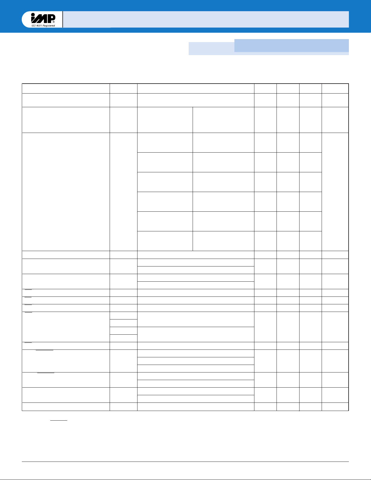
Parameter Symbol Conditions Min Typ Max Units
Input Voltage (VCC) Range V
CC
TA= 0°C to 70°C 1.1 5.5 V
TA= –40°C to 105°C 1.2 5.5
Supply Current (Unloaded) I
CC
TA= –40°C to 85°C V
CC
< 5.5V, L/M/J 6 15 µA
T
A
= –40°C to 85°C V
CC
< 3.6V, R/S/T 5 10
T
A
= 85°C to 105°C V
CC
< 5.5V, L/M/J 25
TA= 85°C to 105°C V
CC
< 3.6V, R/S/T 20
Reset Threshold V
TH
L devices
T
A
= 25°C 4.56 4.63 4.70 V
T
A
= –40°C to 85°C 4.50 4.75
T
A
= 85°C to 105°C 4.40 4.86
M devices
T
A
= 25°C 4.31 4.38 4.45
T
A
= –40°C to 85°C 4.25 4.50
T
A
= 85°C to 105°C 4.16 4.56
J devices
T
A
= 25°C 3.93 4.00 4.06
T
A
= –40°C to 85°C 3.89 4.10
T
A
= 85°C to 105°C 3.80 4.20
T devices
T
A
= 25°C 3.04 3.08 3.11
T
A
= –40°C to 85°C 3.00 3.15
T
A
= 85°C to 105°C 2.92 3.23
S devices
T
A
= 25°C 2.89 2.93 2.96
T
A
= –40°C to 85°C 2.85 3.00
T
A
= 85°C to 105°C 2.78 3.08
R devices
T
A
= 25°C 2.59 2.63 2.66
T
A
= –40°C to 85°C 2.55 2.70
T
A
= 85°C to 105°C 2.50 2.76
Reset Threshold Temp. Coefficient TC
VTH
30 ppm/°C
VCCto Reset Delay VCC= VTHto (VTH- 125mV), L/M/J devices 40 µs
VCC= VTHto (VTH- 125mV), R/S/T devices 20
Reset Active Timeout Period TA= 0°C to 70°C 140 560 ms
TA= –40°C to 105°C 100 840
MR Minimum Pulse Width t
MR
10 µs
MR Glitch Immunity Note 3 100 ns
MR to RESET Propagation Delay t
MD
Note 2 0.5 µs
MR Input Threshold V
IH
VCC> V
TH (MAX)
, IMP811/812L/M/J 2.3 V
V
IL
0.8
V
IH
VCC> V
TH (MAX)
, IMP811/812R/S/T 0.7V
CC
V
IL
0.25V
CC
MR Pull-up Resistance 10 20 30 kΩ
Low RESET Output Voltage (IMP811) V
OL
V
CC
= VTHmin., I
SINK
= 1.2mA, IMP811R/S/T 0.3 V
V
CC
= VTHmin., I
SINK
= 3.2mA, IMP811L/M/J 0.4
VCC> 1.1V, I
SINK
= 50µA 0.3
High RESET Output Voltage (IMP811) V
OH
VCC> VTHmax., I
SOURCE
= 500µA, IMP811R/S/T 0.8V
CC
V
VCC> VTHmax., I
SOURCE
= 800µA, IMP811L/M/J V
CC
-1.5
Low RESET Output Voltage (IMP812) V
OL
VCC= VTHmax., I
SINK
= 1.2mA, IMP812R/S/T 0.3 V
VCC= VTHmax., I
SINK
= 3.2mA, IMP812L/M/J 0.4
High RESET Output Voltage (IMP812) V
OH
1.8V < VCC< VTHmin., I
SOURCE
= 150µA 0.8V
CC
V
Electrical Characteristics
Unless otherwise noted VCCis over the full voltage range, TA= –40°C to 105°C.
Typical values at T
A
= 25°C, VCC= 5V for L/M/J devices, VCC= 3.3V for T/S devices and VCC= 3V for R devices.
Notes: 1. Production testing done at TA= 25°C. Over temperature specifications guaranteed by design only using six sigma design limits.
2. RESET output is active LOW for the IMP811 and RESET output is active HIGH for the IMP812.
3. Glitches of 100ns or less typically will not generate a reset pulse.
Page 4

IMP8
IMP81111
, IMP8
, IMP81122
4
408-432-9100/www.impweb.com
©
1999 IMP, Inc.
Pin Descriptions
Pin Number Name Function
1 GND Ground
2 RESET RESET is asserted LOW if V
CC
falls below the reset threshold and remains LOW for the
(IMP811) 140ms minimum after the reset conditions are removed. In addition, RESET is active LOW
as long as the manual reset is low.
2 RESET RESET is asserted HIGH if V
CC
falls below the reset threshold and remains HIGH for the
(IMP812) 140ms minimum after the reset conditions are removed. In addition, RESET is active
HIGH as long as the manual reset is low.
3 MR Manual Reset Input. A logic LOW on MR asserts RESET. RESET remains active as long
as MR is LOW and for 180ms after MR returns HIGH. The active low input has an internal
20kΩ pull-up resistor. The input should be left open if not used. It can be driven by TTL or
CMOS logic or shorted to ground by a switch..
4V
CC
Power supply input voltage (3.0V, 3.3V, 5.0V)
Related Products
IMP809 IMP810 IMP811 IMP812
Max. Supply Current 15µA 15µA 15µA 15µA
Package Pins 3 3 4 4
Manual RESET input ■■
Package Type SOT-23 SOT-23 SOT-143 SOT-143
Active-HIGH RESET output ■■
Active-LOW RESET output ■■
Page 5

IMP8
IMP81111
, IMP8
, IMP81122
©
1999 IMP, Inc. 408-432-9100/www.impweb.com 5
Detailed Description
Reset Timing and Manual Reset (MR)
The reset signal is asserted–LOW for the IMP811 and HIGH for
the IMP812 – when the V
CC
signal falls below the threshold trip
voltage and remains asserted for 140ms minimum after the V
CC
has risen above the threshold.
A logic low on MR asserts RESET LOW on the IMP811 and HIGH
on the IMP812. MR is internally pulled high through a 20kΩ
resistor and can be driven by TTL/CMOS gates or with open
collector/drain outputs. MR can be left open if not used.
MR may be connected to a normally-open switch connected to
ground without an external debounce circuit.
For added noise rejection, a 0.1µF capacitor from MR to Ground
can be added.
Figure 1. Reset Timing and Manual Reset (MR)
5V
0V
5V
0V
V
CC
V
TH
MR
140ms
minimum
Active Reset
Timeout Period
Active Reset
Timeout Period
5V
0V
RESET
5V
0V
RESET
IMP811
IMP812
811/12_03.eps
Page 6

IMP8
IMP81111
, IMP8
, IMP81122
6
408-432-9100/www.impweb.com
©
1999 IMP, Inc.
RESET Output Operation
In µP/µC systems it is important to have the processor begin
operation from a known state or be able to return the system to a
known state. A RESET output to a processor is provided to prevent improper operation during power supply sequencing or low
voltage – brownout – conditions.
The IMP811/812 are designed to monitor the system power supply voltages and issue a RESET signal when levels are out of
range. RESET outputs are guaranteed to be active for V
CC
above
1.1V. When V
CC
exceeds the reset threshold, an internal timer
keeps RESET active for the reset timeout period, after which
RESET becomes inactive (HIGH for the IMP811 and LOW for the
IMP812).
Valid Reset with VCCunder 1.1V
To ensure that logic inputs connected to the IMP811 RESET pin
are in a known state when V
CC
is under 1.1V, a 100kΩ pull-down
resistor at RESET is needed. The value is not critical.
A similar pull-up resistor to V
CC
is needed with the IMP812.
Negative VCCTransients
Typically short duration transients of 100mV amplitude and 20µs
duration do not cause a false RESET. A 0.1µF capacitor at V
CC
increases transient immunity.
Power
Supply
IMP811
V
CC
GND
RESET
MR
100k
W
811/12_04.eps
Power
Supply
IMP812
V
CC
GND
RESETMR
100kΩ
811/12_05.eps
Application Information
Reset Threshold
Suffix Voltage (V)
L 4.63
M 4.38
J 4.00
T 3.08
S 2.93
R 2.63
Figure 2. RESET Valid with VCCUnder 1.1V Figure 3. RESET Valid with VCCUnder 1.1V
If VCCdrops below the reset threshold, RESET automatically
becomes active. Alternatively, external circuitry or a human operator can initiate this condition using the Manual Reset (MR) pin.
There is an internal pullup on MR so it can be left open if it is not
used. MR can be driven by TTL/CMOS logic or even an external
switch, since it is already debounced. If the switch is at the end of
a long cable, it might require a bypass (100nF) at the pin if noise
pickup is a problem.
Six voltage thresholds are available to support 3V and 5V systems:
Page 7

IMP8
IMP81111
, IMP8
, IMP81122
©
1999 IMP, Inc. 408-432-9100/www.impweb.com 7
Bi-directional Reset Pin Interfacing
The IMP811/812 can interface with µP/µC bi-directional reset
pins by connecting a 4.7kΩ resistor in series with the IMP809/810
reset output and the µP/µC bi-directional reset pin.
Power
Supply
IMP811
V
CC
GND GND
RESET
4.7k
W
811/12_06.eps
Bi-directional I/O Pin
(Example: 68HC11)
BUF
Buffered
RESET
m
C or mP
RESET
Input
MR
Figure 4. Bi-directional Reset Pin Interface
Plastic SOT-143 (4-Pin)
E
A
C
L
e
A1
H
D
e
e1
B
B1
a = 0°-8°
SOT-143 (4-Pin).eps
Inches Millimeters
Min Max Min Max
Plastic SOT-143 (4-Pin)
A 0.031 0.047 0.787 1.194
A1 0.001 0.005 0.025 0.127
B 0.014 0.022 0.356 0.559
B1 0.030 0.038 0.762 0.965
C 0.0034 0.006 0.086 0.152
D 0.105 0.120 2.667 3.048
E 0.047 0.055 1.194 1.397
e 0.070 0.080 1.778 2.032
e1 0.071 0.079 1.803 2.007
H 0.082 0.098 2.083 2.489
I 0.004 0.012 0.102 0.305
Package Dimensions
Application Information
Page 8

IMP8
IMP81111
, IMP8
, IMP81122
IMP, Inc.
Corporate Headquarters
2830 N. First Street
San Jose, CA 95134-2071
Tel: 408-432-9100
Tel: 800-438-3722
Fax: 408-434-0335
e-mail: info@impinc.com
http://www.impweb.com
The IMP logo is a registered trademark of IMP, Inc.
All other company and product names are trademarks of their respective owners.
© 1999 IMP, Inc.
Printed in USA
Publication #: 1019
Revision: A
Issue Date: 08/17/99
Type: Preliminary
 Loading...