

Datasheet IMP810TEUR-T, IMP810SEUR-T, IMP810REUR-T, IMP810LEUR-T, IMP810JEUR-T Datasheet (IMP)
...Page 1
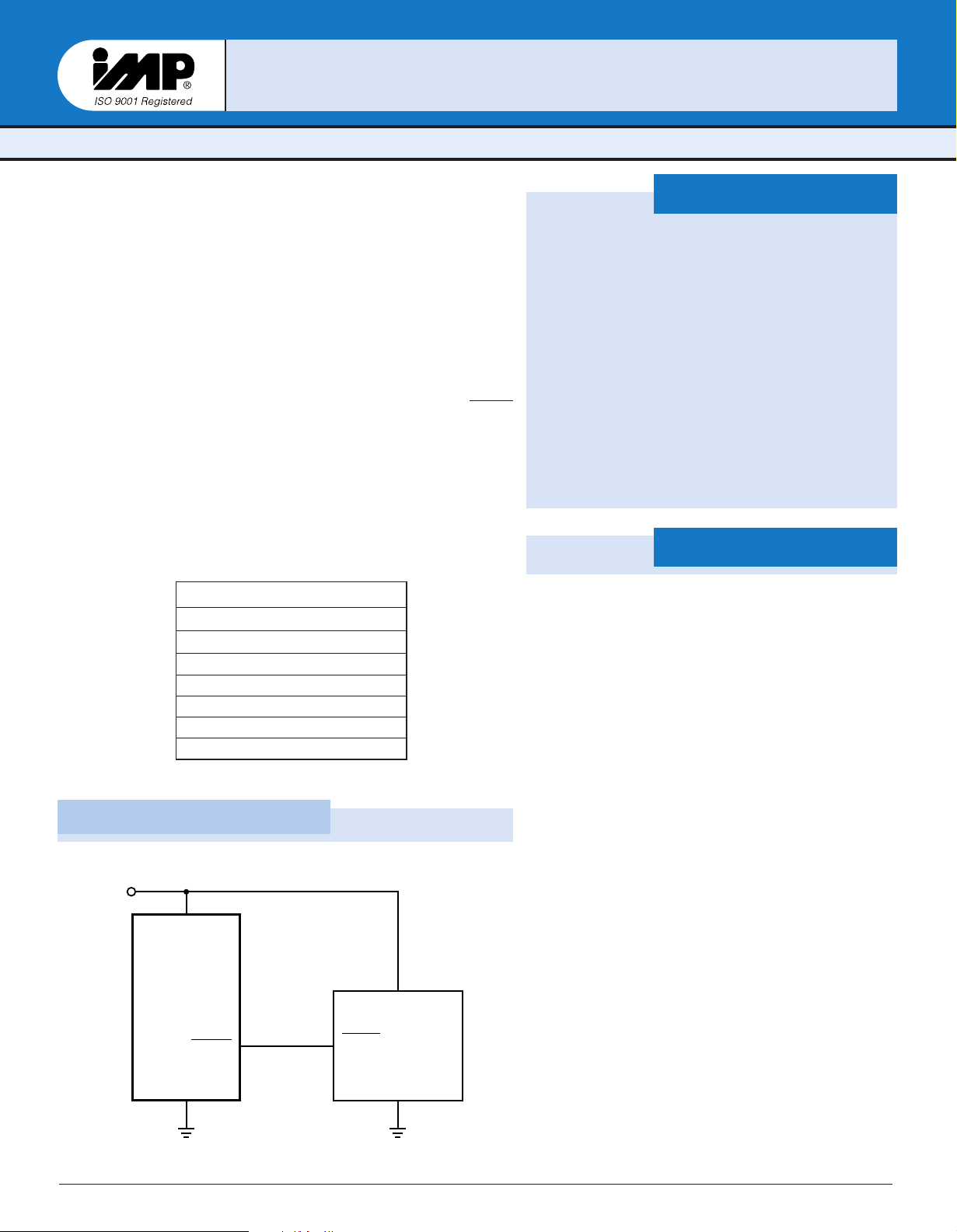
IMP809
(IMP810)
V
CC
V
CC
V
CC
GND GND
RESET
(RESET)
809/10_01.eps
µP
RESET
Input
POWER MANAGEMENT
IMP809, IMP81100
IMP809, IMP8
3-Pin Microcontroller
Power Supply Supervisor
The IMP809/IMP810 are 3.0V, 3.3V and 5.0V power supply supervisor circuits optimized for low-power microprocessor (µP), microcontroller (µC)
and digital systems. The IMP809/810 are improved drop-in replacements
for the Maxim MAX809/810 and feature 60% lower supply current.
A reset signal is issued if the power supply voltage drops below a preset
reset threshold and is asserted for at least 140ms after the supply has
risen above the reset threshold. The IMP809 has an active-low RESET
output that is guaranteed to be in the correct state for V
The IMP810 has an active-high RESET output. The reset comparator is
designed to ignore fast transients on V
Low supply current makes the IMP809/IMP810 ideal for use in portable
and battery operated equipment. The IMP809/IMP810 are available in a
compact 3-pin SOT23 package.
Six voltage thresholds are available to support 3V to 5V systems:
CC
.
Reset Threshold
Suffix Voltage (V)
L 4.63
M 4.38
J 4.00
T 3.08
S 2.93
R 2.63
down to 1.1V.
CC
Key Features
◆
Improved Maxim MAX809/MAX810 replacement
— Lower supply current…6µA
— 80% lower maximum supply current
◆
Monitor 5V, 3.3V and 3V supplies
◆
140ms min. reset pulse width
◆
Active-low reset valid with 1.1V supply
(IMP809)
◆
Small 3-pin SOT-23 package
◆
No external components
◆
Specified over full temperature range
— –40°C to 105°C
Applications
◆ Embedded controllers
◆ Battery operated systems
◆ Intelligent instruments
◆ Wireless communication systems
◆ PDAs and handheld equipment
Block Diagrams
IMP, Inc. San Jose, CA 408-432-9100/www.impweb.com
Page 2
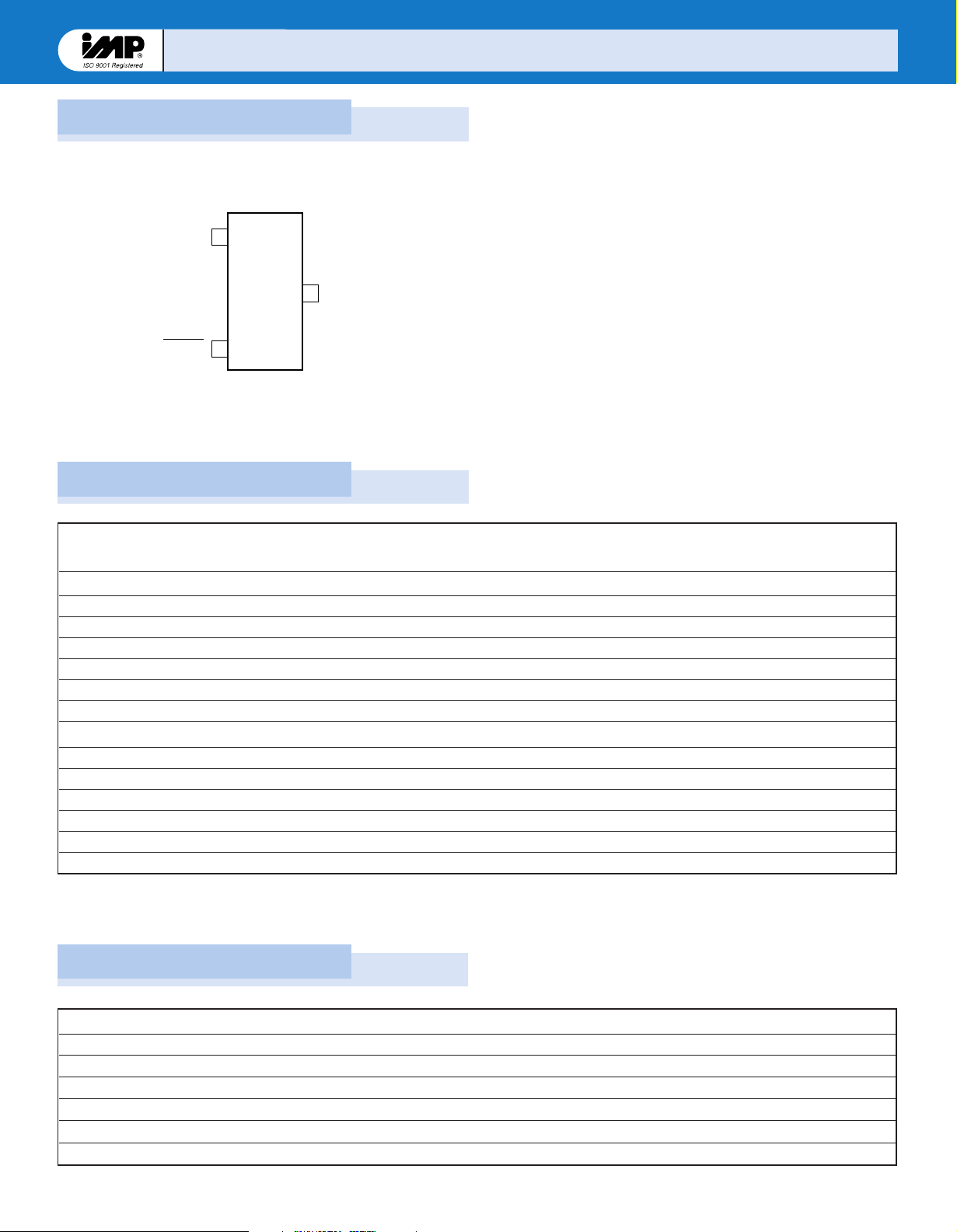
Pin Configuration
IMP809
(IMP810)
GND
(RESET) RESET
V
CC
3
1
2
809/10_02.eps
SOT23
Ordering Information
IMP809, IMP81100
IMP809, IMP8
Package Marking
Part Number
1
Reset Threshold (V) Temperature Range Pin-Package
(XX Lot Code)
IMP809 Active LOW Reset
IMP809LEUR-T 4.63 –40°C to +105°C 3-SOT23 AAXX
IMP809MEUR-T 4.38 –40°C to +105°C 3-SOT23 ABXX
IMP809JEUR-T 4.00 –40°C to +105°C 3-SOT23 CWXX
IMP809TEUR-T 3.08 –40°C to +105°C 3-SOT23 ACXX
IMP809SEUR-T 2.93 –40°C to +105°C 3-SOT23 ADXX
IMP809REUR-T 2.63 –40°C to +105°C 3-SOT23 AFXX
IMP810 Active HIGH Reset
IMP810LEUR-T 4.63 –40°C to +105°C 3-SOT23 AGXX
IMP810MEUR-T 4.38 –40°C to +105°C 3-SOT23 AHXX
IMP810JEUR-T 4.00 –40°C to +105°C 3-SOT23 AIXX
IMP810TEUR-T 3.08 –40°C to +105°C 3-SOT23 AJXX
IMP810SEUR-T 2.93 –40°C to +105°C 3-SOT23 AKXX
IMP810REUR-T 2.63 –40°C to +105°C 3-SOT23 ALXX
Notes: 1. Tape and Reel packaging is indicated by the -T designation.
2. Devices may also be marked with full part number: 809L, 810M etc. XX refers to lot.
Related Products
2
IMP809 IMP810 IMP811 IMP812
Max. Supply Current 15µA 15µA 15µA 15µA
Package Pins 3 3 4 4
Manual RESET input ■ ■
Package Type SOT-23 SOT-23 SOT-143 SOT-143
Active-HIGH RESET output ■ ■
Active-LOW RESET output ■ ■
2
2
Page 3
IMP809, IMP81100
IMP809, IMP8
Absolute Maximum Ratings
Pin Terminal Voltage with Respect to Ground
V
. . . . . . . . . . . . . . . . . . . . . . . . . . . . . . . . . –0.3V to 6.0V
CC
RESET, RESET . . . . . . . . . . . . . . . . . . . . . . . . . –0.3V to (V
Input Current at V
. . . . . . . . . . . . . . . . . . . 20mA
CC
Output Current: RESET, RESET . . . . . . . . . 20mA
Rate of Rise at V
. . . . . . . . . . . . . . . . . . . . 100V/µs
CC
CC
+ 0.3V)
Power Dissipation (T
(Derate 4mW/°C above 70
= 70°C) . . . . . . . . . . 320mW
A
°C)
Operating Temperature Range . . . . . . . . . . –40°C to 105°C
Storage Temperature Range . . . . . . . . . . . . . –65°C to 160°C
Lead Temperature (soldering, 10 sec) . . . . . 300°C
These are stress ratings only and functional operation is not implied.
Exposure to absolute maximum ratings for prolonged time periods may
affect device reliability
Electrical Characteristics
Unless otherwise noted VCCis over the full voltage range, TA= –40°C to 105°C.
Typical values at T
Parameter Symbol Conditions Min Typ Max Units
Input Voltage (VCC) Range V
Supply Current I
Reset Threshold V
Reset Threshold Stability 30 ppm/°C
VCCto Reset Delay VCC= VTHto VTH- 100mV 20 µs
Reset Active Timeout Period V
Low RESET Output Voltage (IMP809) V
High RESET Output Voltage (IMP809) V
Low RESET Output Voltage (IMP810) V
High RESET Output Voltage (IMP810) V
Notes:
1. Production testing done at TA= 25°C. Over-temperature specifications guaranteed by design only.
2.RESET output is active LOW for the IMP809 and RESET output is active HIGH for the IMP810
= 25°C, VCC= 5V for L/M/J devices, VCC= 3.3V for T/S devices and VCC= 3V for R devices.
A
CC
TA= 0°C to 70°C 1.1 5.5 V
TA= –40°C to 105°C 1.2 5.5
CC
TA= –40°C to 85°C V
T
= –40°C to 85°C V
A
T
= 85°C to 105°C V
A
TA= 85°C to 105°C V
L devices
TH
M devices
J devices
T devices
S devices
R devices
TA= –40°C to 85°C 140 240 560 ms
OL
< 5.5V, L/M/J 9 15 µA
CC
< 3.6V, R/S/T 6 10
CC
< 5.5V, L/M/J 25
CC
< 3.6V, R/S/T 20
CC
= 25°C 4.56 4.63 4.70 V
T
A
= –40°C to 85°C 4.50 4.75
T
A
= 85°C to 105°C 4.40 4.86
T
A
= 25°C 4.31 4.38 4.45
T
A
= –40°C to 85°C 4.25 4.50
T
A
= 85°C to 105°C 4.16 4.56
T
A
= 25°C 3.93 4.00 4.06
T
A
= –40°C to 85°C 3.89 4.10
T
A
= 85°C to 105°C 3.80 4.20
T
A
= 25°C 3.04 3.08 3.11
T
A
= –40°C to 85°C 3.00 3.15
T
A
= 85°C to 105°C 2.92 3.23
T
A
= 25°C 2.89 2.93 2.96
T
A
= –40°C to 85°C 2.85 3.00
T
A
= 85°C to 105°C 2.78 3.08
T
A
= 25°C 2.59 2.63 2.66
T
A
= –40°C to 85°C 2.55 2.70
T
A
= 85°C to 105°C 2.50 2.76
T
A
TA= 85°C to 105°C 100 840
V
OH
OL
OH
OL
= VTHmin., I
CC
V
= VTHmin., I
CC
VCC> 1.1V, I
VCC> VTHmax., I
VCC> VTHmax., I
VCC= VTHmax., I
VCC= VTHmax., I
1.8V < VCC< VTHmin., I
SINK
= 1.2mA, IMP809R/S/T 0.3 V
SINK
= 3.2mA, IMP809L/M/J 0.4
SINK
= 50µA 0.3
= 500µA, IMP809R/S/T 0.8V
SOURCE
= 800µA, IMP809L/M/J V
SOURCE
= 1.2mA, IMP810R/S/T 0.3 V
SINK
= 3.2mA, IMP810L/M/J 0.4
SINK
= 150µA 0.8V
SOURCE
CC
CC
-1.5
CC
V
V
3
Page 4
IMP809, IMP81100
IMP809, IMP8
Pin Descriptions
Pin Number Name Function
1 GND Ground
2 RESET RESET is asserted LOW if V
(IMP809) 240ms typical reset timeout period (140ms minimum) after VCCexceeds the threshold.
2 RESET RESET is asserted HIGH if V
(IMP810) 240ms typical reset timeout period (140ms minimum) after VCCexceeds the threshold.
3 V
CC
Power supply input voltage (3.0V, 3.3V, 5.0V)
falls below the reset threshold and remains LOW for the
CC
falls below the reset threshold and remains HIGH for the
CC
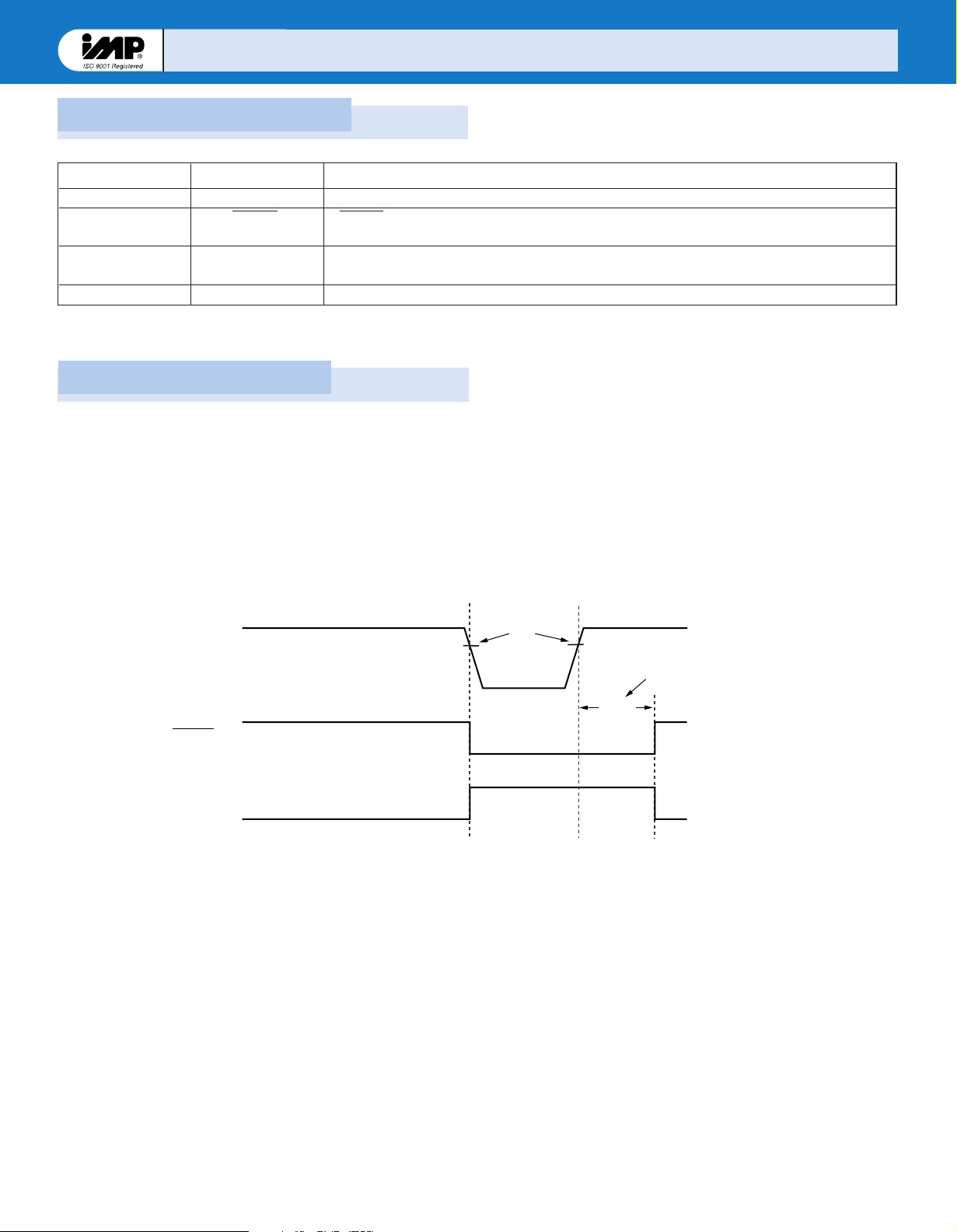
Detailed Descriptions
Reset Timing
The reset signal is asserted–LOW for the IMP809 and HIGH for the
IMP810–when the V
and remains asserted for 140ms minimum after the V
above the threshold.
signal falls below the threshold trip voltage
CC
has risen
CC
V
CC
RESET
RESET
5V
0V
5V
0V
5V
0V
V
TH
Figure 1. Reset Timing Diagram
Active Reset
Timeout Period
140ms
minimum
IMP809
IMP810
809/10_03.eps
4
Page 5
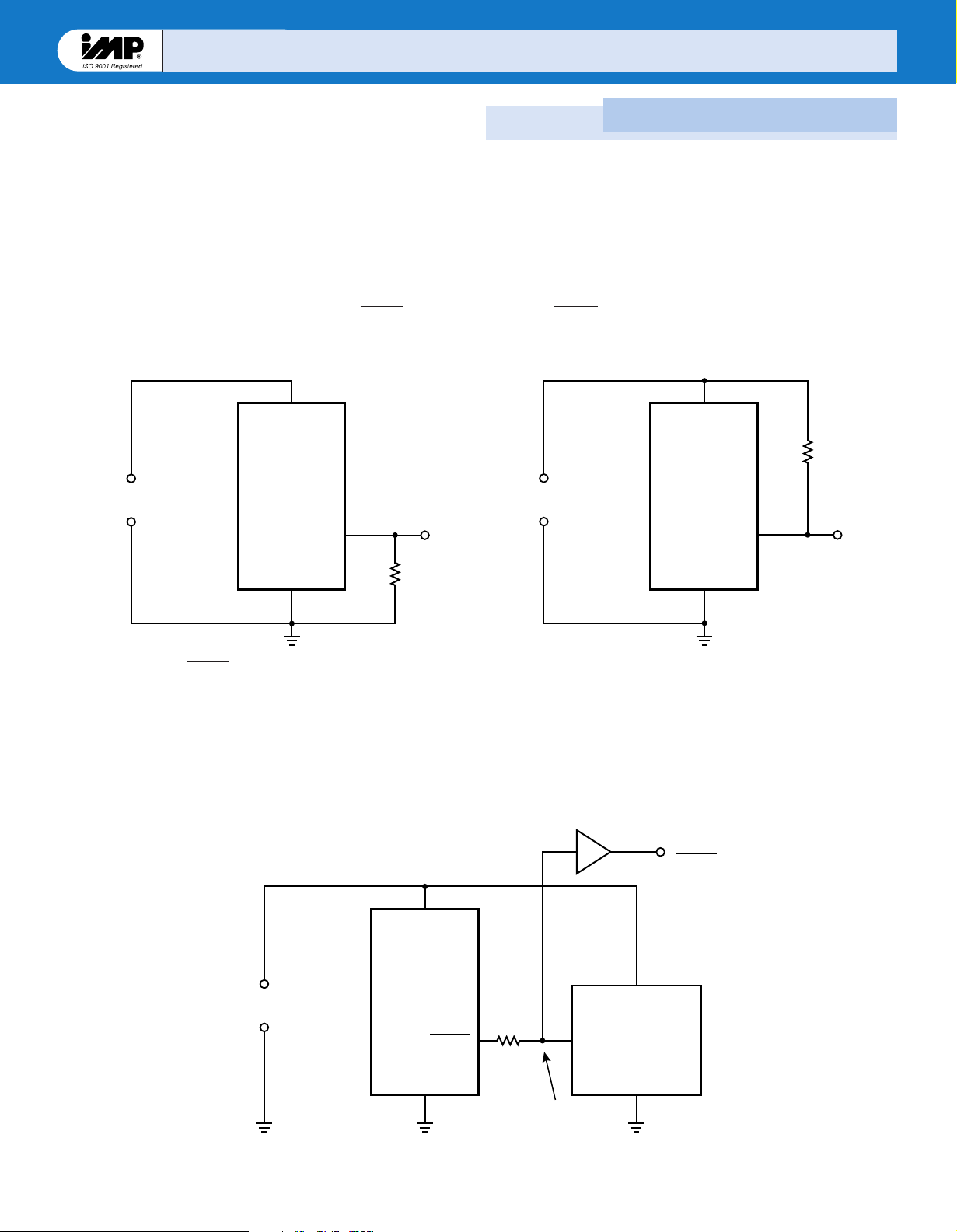
Negative VCCTransients
Power
Supply
IMP810
V
CC
GND
RESET
100kΩ
809/10_05.eps
Power
Supply
IMP809
V
CC
GND
RESET
100kΩ
809/10_04.eps
Power
Supply
IMP809
V
CC
GND GND
RESET
4.7kΩ
809/10_06.eps
Bi-directional I/O Pin
(Example: 68HC11)
BUF
Buffered
RESET
µC or µP
RESET
Input
The IMP809/810 protect µPs from brownouts and low VCC. Short
duration transients of 100mV amplitude and 20µs or less duration
typically do not cause a false RESET.
Valid Reset with VCCunder 1.1V
IMP809, IMP81100
IMP809, IMP8
Application Information
To ensure logic inputs connected to the IMP809 RESET pin are in
a known state when V
is under 1.1V, a 100kΩ pull-down
CC
Figure 2. RESET Valid with VCCUnder 1.1V
Bi-directional Reset Pin Interfacing
The IMP809/810 can interface with µP/µC bi-directional reset
pins by connecting a 4.7kΩ resistor in series with the
IMP809/810 reset output and the µP/µC bi-directional reset pin.
resistor at RESET is needed. The value is not critical. A pull-up
resistor to VCCis needed with the IMP810.
Figure 3. RESET Valid with V
Under 1.1V
CC
Figure 4. Bi-directional Reset Pin Interfacing
5
Page 6
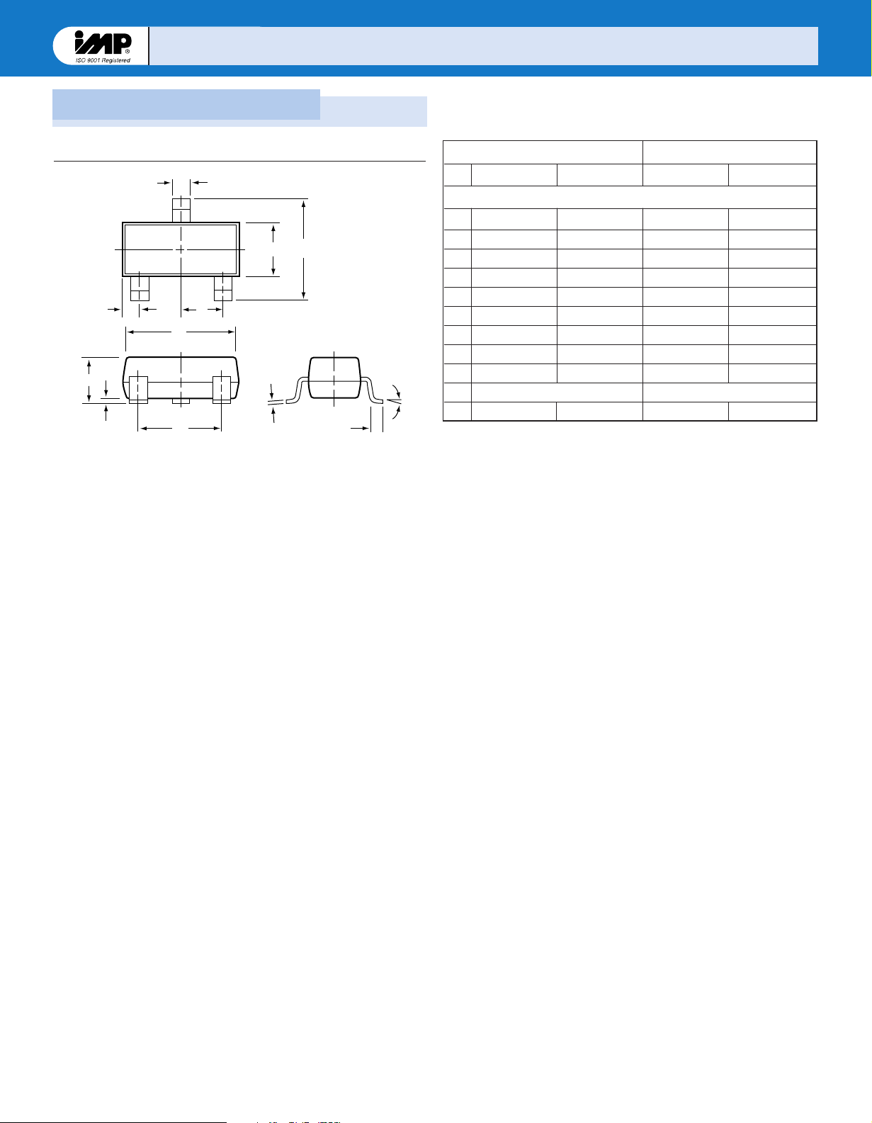
Package Dimensions
E
A
C
L
e1
A1
H
e
D
S
B
a
SOT-23 (3-Pin).eps
IMP809, IMP81100
IMP809, IMP8
Plastic SOT-23 (3-Pin)
Inches Millimeters
Min Max Min Max
Plastic SOT-23 (3-Pin)
A 0.031 0.050 0.80 1.27
A1 0.004 0.010 0.10 0.25
B 0.015 0.020 0.37 0.51
C 0.003 0.007 0.085 0.18
D 0.110 0.120 2.80 3.04
E 0.047 0.055 1.20 1.40
e 0.035 0.040 0.89 1.03
e1 0.070 0.080 1.78 2.05
H 0.083 0.1039 2.10 2.64
L 0.027 REF 0.069 REF
S 0.018 0.024 0.45 0.60
6
Page 7

IMP809, IMP81100
IMP809, IMP8
IMP, Inc.
Corporate Headquarters
2830 N. First Street
San Jose, CA 95134-2071
Tel: 408-432-9100
Tel: 800-438-3722
Fax: 408-434-0335
Fax-on-Demand: 1-800-249-1614 (USA)
Fax-on-Demand: 1-303-575-6156 (International)
e-mail: info@impinc.com
http://www.impweb.com
The IMP logo is a registered trademark of IMP, Inc.
All other company and product names are trademarks of their respective owners.
© 1998 IMP, Inc.
Printed in USA
Preliminary
Part No.: IMP809-810
Document Number: IMP809-6-6/98
7
 Loading...