

Page 1
©
1999 IMP, Inc. 408-432-9100/www.impweb.com
1
Key Features
Applications
◆ Computers and controllers
◆ CTI applications
◆ Embedded controllers
◆ Battery operated systems
◆ Intelligent instruments
◆ Wireless communication systems
◆ PDAs and handheld equipment
◆
Lower power, pin compatible replacements for
Maxim MAX706P/R/S/T, MAX708R/S/T
– 30% lower supply current:140µA vs. 200µA
◆
Precision power supply monitor
– 2.63V threshold (IMP706P/R, IMP708R)
– 2.93V threshold (IMP706S, IMP708S)
– 3.08V threshold (IMP706T, IMP708T)
– New 4.00V threshold (IMP706J, IMP708J)
◆
Debounced manual reset input
◆
Auxiliary voltage monitor comparator
– 1.25V threshold
– Battery monitor/auxiliary supply monitor
◆
Watchdog timer (IMP706P/R/S/T/J)
– Watchdog can be disabled by floating WDI
◆
200ms reset time delay
◆
Three reset signal options
– Active HIGH: IMP706P
– Active LOW: IMP706R/S/T/J
– Active HIGH & LOW outputs: IMP708R/S/T/J
◆
DIP, SO and MicroSO packages
◆
Guaranteed RESET assertion to VCC= 1.1V
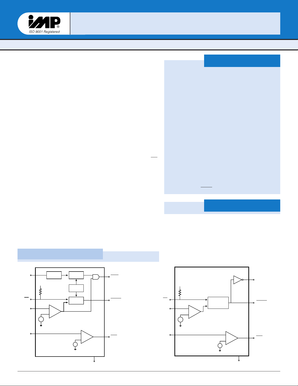
Block Diagrams
IMP706P/R/S/T/J, IMP708R/S/T/J
IMP706P/R/S/T/J, IMP708R/S/T/J
POWER MANAGEMENT
3/3.3/4.0V
3/3.3/4.0V µµ
P Super
P Super
visor Cir
visor Cir
cuits
cuits
– Lo
– Lo
w suppl
w suppl
y cur
y currr
ent
ent
– W
– W
atc
atc
hdog timer
hdog timer
– Br
– Broo
wnout det
wnout det
ection
ection
The IMP706P/R/S/T/J and IMP708R/S/T/J CMOS supervisor circuits
monitor power-supply and battery voltage level, and µP/µC operation.
A reset is generated when the supply drops below 2.63V (IMP706P/R,
IMP708R), 2.93V (IMP706S, IMP708S), 3.08V (IMP706T, IMP708T) or 4.00
(IMP706J, IMP708J).
The family offers several functional options. Each device generates a
reset signal during power-up, power-down and during brownout
conditions.
In addition, the IMP706P/R/S/T/J feature a 1.6 second watchdog timer.
The watchdog timer output will trigger a reset if connected to MR.
Unlike competitive devices, floating the WDI input pin disables the
watchdog timer.
The IMP708R/S/T/J have both active-HIGH and active-LOW reset outputs but no watchdog function. The IMP706P has the same pin-out and
functions as the IMP706R but has an active-HIGH reset output.
A versatile power-fail circuit, useful in checking battery levels and
non-5V supplies, has a 1.25V threshold. All devices have a manual
reset input.
All devices are available in 8-pin DIP, SO and the compact MicroSO
packages. The MicroSO package requires 50% less PC board area than
the conventional SO package.
WDI
MR
V
PFI
V
CC
20kΩ
CC
+
IMP706P/R/S/T/J
Transition
Detector
+
–
2.63V (IMP706P/R)
2.93V (IMP706S)
3.08V (IMP706T)
4.00V (IMP706J)
Watchdog
Timebase
Generator
1.25V
Timer
RESET
WDO
RESET
(RESET) IMP706P
+
–
GND
PFO
706P_01.eps
V
CC
20kΩ
V
MR
PFI
CC
+
+
–
2.63V (IMP708R)
2.93V (IMP708S)
3.08V (IMP708T)
4.00V (IMP708J)
IMP708R/S/T/J
RESET
Generator
1.25V
RESET
RESET
+
–
GND
PFO
706P_02.eps
Page 2
2
408-432-9100/www.impweb.com
©
1999 IMP, Inc.
Ordering Information
Pin Configuration
IMP706P/R/S/T/J, IMP708R/S/T/J
IMP706P/R/S/T/J, IMP708R/S/T/J
IMP708R/S/T/J
1
2
3
4
MR
V
CC
GND
PFI
RESET
RESET
NC
PFO
8
7
6
5
IMP706P
1
2
3
4
MR
V
CC
GND
PFI
WDO
RESET
WDI
PFO
8
7
6
5
IMP706R/S/T/J
1
2
3
4
MR
V
CC
GND
PFI
WDO
RESET
WDI
PFO
8
7
6
5
IMP706P
IMP706R/S/T/J
1
2
3
4
(RESET) RESET
(IMP706P)
WDO
MR
V
CC
WDI
PFO
PFI
GND
8
7
6
5
IMP708R/S/T/J
1
2
3
4
RESET
RESET
MR
V
CC
NC
PFO
PFI
GND
8
7
6
5
706P_03.eps
DIP/SO
MicroSO
Operating
Part Number Package Temperature Range Reset Threshold Reset Polarity Watchdog Timer
IMP706PCPA 8-Plastic DIP 0°C to +70°C 2.63 HIGH YES
IMP706PCSA 8-SO 0°C to +70°C 2.63 HIGH YES
IMP706PCUA 8-MicroSO 0°C to +70°C 2.63 HIGH YES
IMP706PEPA 8-Plastic DIP –40°C to +85°C 2.63 HIGH YES
IMP706PESA 8-SO –40°C to +85°C 2.63 HIGH YES
IMP706RCPA 8-Plastic DIP 0°C to +70°C 2.63 LOW YES
IMP706RCSA 8-SO 0°C to +70°C 2.63 LOW YES
IMP706RCUA 8-MicroSO 0°C to +70°C 2.63 LOW YES
IMP706REPA 8-Plastic DIP –40°C to +85°C 2.63 LOW YES
IMP706RESA 8-SO –40°C to +85°C 2.63 LOW YES
IMP706SCPA 8-Plastic DIP 0°C to +70°C 2.93 LOW YES
IMP706SCSA 8-SO 0°C to +70°C 2.93 LOW YES
IMP706SCUA 8-MicroSO 0°C to +70°C 2.93 LOW YES
IMP706SEPA 8-Plastic DIP –40°C to +85°C 2.93 LOW YES
IMP706SESA 8-SO –40°C to +85°C 2.93 LOW YES
IMP706TCPA 8-Plastic DIP 0°C to +70°C 3.08 LOW YES
IMP706TCSA 8-SO 0°C to +70°C 3.08 LOW YES
IMP706TCUA 8-MicroSO 0°C to +70°C 3.08 LOW YES
IMP706TEPA 8-Plastic DIP –40°C to +85°C 3.08 LOW YES
IMP706TESA 8-SO –40°C to +85°C 3.08 LOW YES
IMP706JCPA 8-Plastic DIP 0°C to +70°C 4.00 LOW YES
IMP706JCSA 8-SO 0°C to +70°C 4.00 LOW YES
IMP706JCUA 8-MicroSO 0°C to +70°C 4.00 LOW YES
IMP706JEPA 8-Plastic DIP –40°C to +85°C 4.00 LOW YES
IMP706JESA 8-SO –40°C to +85°C 4.00 LOW YES
IMP708RCPA 8-Plastic DIP 0°C to +70°C 2.63 Dual: HIGH & LOW NO
IMP708RCSA 8-SO 0°C to +70°C 2.63 Dual: HIGH & LOW NO
IMP708RCUA 8-MicroSO 0°C to +70°C 2.63 Dual: HIGH & LOW NO
IMP708REPA 8-Plastic DIP –40°C to +85°C 2.63 Dual: HIGH & LOW NO
IMP708RESA 8-SO –40°C to +85°C 2.63 Dual: HIGH & LOW NO
IMP708SCPA 8-Plastic DIP 0°C to +70°C 2.93 Dual: HIGH & LOW NO
IMP708SCSA 8-SO 0°C to +70°C 2.93 Dual: HIGH & LOW NO
IMP708SCUA 8-MicroSO 0°C to +70°C 2.93 Dual: HIGH & LOW NO
IMP708SEPA 8-Plastic DIP –40°C to +85°C 2.93 Dual: HIGH & LOW NO
IMP708SESA 8-SO –40°C to +85°C 2.93 Dual: HIGH & LOW NO
IMP708TCPA 8-Plastic DIP 0°C to +70°C 3.08 Dual: HIGH & LOW NO
IMP708TCSA 8-SO 0°C to +70°C 3.08 Dual: HIGH & LOW NO
IMP708TCUA 8-MicroSO 0°C to +70°C 3.08 Dual: HIGH & LOW NO
IMP708TEPA 8-Plastic DIP –40°C to +85°C 3.08 Dual: HIGH & LOW NO
IMP708TESA 8-SO –40°C to +85°C 3.08 Dual: HIGH & LOW NO
IMP708JCPA 8-Plastic DIP 0°C to +70°C 4.00 Dual: HIGH & LOW NO
IMP708JCSA 8-SO 0°C to +70°C 4.00 Dual: HIGH & LOW NO
IMP708JCUA 8-MicroSO 0°C to +70°C 4.00 Dual: HIGH & LOW NO
IMP708JEPA 8-Plastic DIP –40°C to +85°C 4.00 Dual: HIGH & LOW NO
IMP708JESA 8-SO –40°C to +85°C 4.00 Dual: HIGH & LOW NO
Page 3
Pin Terminal Voltage with Respect to Ground
V
CC
. . . . . . . . . . . . . . . . . . . . . . . . . . . . . . . . . –0.3V to 6.0V
All other inputs . . . . . . . . . . . . . . . . . . . . . . . . – 0.3V to (V
CC
+ 0.3V)
Input Current at V
CC
and GND . . . . . . . . . . 20mA
Output Current: All outputs . . . . . . . . . . . . . 20mA
Rate of Rise at V
CC
. . . . . . . . . . . . . . . . . . . . . 100V/µs
Plastic DIP Power Dissipation . . . . . . . . . . . 700mW
(Derate 9mW/°C above 70°C)
SO Power Dissipation . . . . . . . . . . . . . . . . . . 470mW
(Derate 5.9mW/°C above 70°C)
MicroSO Power Dissipation . . . . . . . . . . . . . 330mW
(Derate 4.1mW/°C above 70°C)
Operating Temperature Range
IMP706xE, IMP708xE . . . . . . . . . . . . . . . . . . – 40°C to +85°C
IMP706xC, IMP708xC . . . . . . . . . . . . . . . . . . 0°C to +70°C
Storage Temperature Range . . . . . . . . . . . . . . –65°C to +160°C
Lead Temperature Soldering (10 sec) . . . . . . 300°C
These are stress ratings only and functional operation is not implied.
Exposure to absolute maximum ratings for prolonged time periods may
affect device reliability.
©
1999 IMP, Inc. 408-432-9100/www.impweb.com
3
IMP706P/R/S/T/J, IMP708R/S/T/J
IMP706P/R/S/T/J, IMP708R/S/T/J
Absolute Maximum Ratings
Electrical Characteristics
Unless otherwise noted, specifications are over the operating temperature range and VCCsupply voltages are 2.7V to 5.5V (IMP706P,
IMP708R), 3.0V to 5.5V (IMP706/8S), 3.15V to 5.5V (IMP706/8T) and 4.1V to 5.5V (IMP706/8J).
retemaraPlobmySsnoitidnoCniMpyTxaMstinU
egatloVgnitarepO
egnaR
V
CC
Cx807PMI,Cx607PMI
Ex807PMI,Ex607PMI
1.1
2.1
5.5
5.5
V
tnerruCylppuS
V
CC
V6.3<
I
CC
V=RM,Ex607PMI,Cx607PMI
CC
gnitaolFIDW,57041
µA
V=RM,Ex807PMI,Cx807PMI
CC
gnitaolFIDW,05041
tnerruCylppuS
V
CC
V5.5<
I
CC
V=RM,Ex607PMI,Cx607PMI
CC
gnitaolFIDW,57041
µA
V=RM,Ex807PMI,Cx807PMI
CC
gnitaolFIDW,05041
dlohserhTTESERV
TR
secivedRdnaP
secivedS
secivedT
secivedJ
55.2
58.2
00.3
98.3
36.2
39.2
80.3
00.4
07.2
00.3
51.3
01.4
V
dlohserhTTESER
siseretsyH
04Vm
htdiWesluPTESERt
SR
V
CC
,)secivedR/P,8/607PMI(V3=
V
CC
)secivedT/S,8/607PMI(V3.3=
V
CC
)secivedJ,8/607PMI(V4.4=
041002082sm
V
CC
V5=002
htdiWesluPRMt
RM
V<V5.4
CC
V5.5<051sn
V<V6.3
CC
)secivedJ8/607PMI(V5.4<
V
)XAM(TSR
V<
CC
)secivedT/S/R/P8/607PMI(V6.3<
005
yaleDtuOTESERotRMt
DM
V<V6.3
CC
)secivedJ8/607PMI(V5.4<
V
)XAM(TSR
V<
CC
)secivedT/S/R/P8/607PMI(V6.3<
057sn
V<V5.4
CC
V5.5<052
dlohserhTtupnIRMV
HI
V
)XAM(TSR
V<
CC
V5.4<V7.0
CC
V
V
LI
V
)XAM(TSR
V<
CC
V5.4<6.0
V
HI
V<V5.4
CC
V5.5<0.2
V
LI
V<V5.4
CC
V5.5<8.0
rotsiseRpu-lluPRMR
P
010204kΩ
egatloVtuptuOTESER
)secivedJ/T/S/RllA(
V
HO
I
ECRUOS
008= µ V<V5.4,A
CC
V5.5<V
CC
V5.1– V
V
LO
I
KNIS
V<V5.4,Am2.3=
CC
V5.5<4.0
V
HO
I
ECRUOS
005= µ V,A
)XAM(TSR
V<
CC
V5.4<V8.0
CC
V
LO
I
KNIS
V,Am2.1=
)XAM(TSR
V<
CC
V5.4<3.0
V
LO
I
KNIS
05= µ V,A
CC
)secivedCx807PMI,Cx607PMI(V1.1=3.0
I
KNIS
001= µ V,A
CC
)secivedEx807PMI,Ex607PMI(V2.1=3.0
Page 4

IMP706P/R/S/T/J, IMP708R/S/T/J
IMP706P/R/S/T/J, IMP708R/S/T/J
4
408-432-9100/www.impweb.com
©
1999 IMP, Inc.
Unless otherwise noted, specifications are over the operating temperature range and VCCsupply voltages are 2.7V to 5.5V (IMP706P,
IMP708R), 3.0V to 5.5V (IMP706/8S), 3.15V to 5.5V (IMP706/8T) and 4.1V to 5.5V (IMP706/8J).
Electrical Characteristics
(cont.)
retemaraPlobmySsnoitidnoCniMpyTxaMstinU
P607PMI
egatloVtuptuOTESER
,egatloVtuptuOTESER
J/T/S/R807PMI
doirePtuoemiTgodhctaWt
htdiWesluPIDWt
htdiWesluPIDWt
dlohserhTtupnIIDWV
tnerruCtupnIIDW
tnerruCtupnIIDW
egatloVtuptuOODW
dlohserhTtupnIIFPVsecivedR/ProF.gnillafIFP
tnerruCtupnIIFP 52– 10.052An
egatloVtuptuOOFPV
V
V
V
V
V
V
V
V
V
V
V
V
V
V
V
V
V
V
I
HO
I
LO
HO
LO
HO
LO
HO
LO
DW
PW
PW
HI
LI
HI
LI
HO
LO
HO
LO
HO
LO
HO
LO
KNIS
I
I
KNIS
I
I
KNIS
I
I
KNIS
V
CC
V
CC
V
CC
V
LI
V
LI
V
CC
V
I
I
KNIS
I
I
KNIS
I
I
KNIS
I
I
KNIS
008= µ V<V5.4,A
ECRUOS
V<V5.4,Am2.3=
CC
005= µ V,A
ECRUOS
V,Am2.1=
008= µ V<V5.4,A
ECRUOS
005= µ V,A
ECRUOS
V,Am2.1=
)XAM(TSR
V<V5.4,Am2.3=
CC
)XAM(TSR
V5.5<V
CC
CC
V5.5<
V<
)XAM(TSR
V<
CC
CC
V6.3<V8.0
CC
V6.3<3.0
V5.5<V
CC
V5.5<
V<
)XAM(TSR
V<
CC
)secivedR/P,607PMI(V3=
V5.4<V8.0
CC
V5.4<3.0
0.16.152.2s
V5.1– V
4.0
CC
V5.1– V
4.0
CC
)secivedT/S,607PMI(V3.3=
)secivedJ,607PMI(V4.4=
V,V4.0=
V,V4.0=
V8.0=
HI
HI
V,
CC
V8.0=
CC
V<
)XAM(TSR
V<V5.4,
CC
V5.4<001sn
CC
V5.5<05sn
V5=5.3V
8.0
V<
)XAM(TSR
V5.4<
CC
V7.0
CC
6.0
V=IDW
CC
008= µ V<V5.4,A
ECRUOS
005= µ V,A
ECRUOS
005= µ V,A
Vsecived
CC
008= µ V<V5.4,A
ECRUOS
005= µ V,A
ECRUOS
V,Am2.1=
ylnO607PMI,
ylnO607PMI,V0=IDW
V5.5<V
CC
V<V5.4,Am2.1=
V<V5.4,Am2.3=
)XAM(SR
V5.5<4.0
CC
V<
)XAM(TSR
V<
)XAM(TSR
CC
CC
CC
V5.5<4.0
CC
V<
)XAM(SR
CC
V<
CC
V5.4<
CC
V5.4<3.0
T/SroF.V3=
VsecivedJroF.V3.3=
CC
.V4.4=
V5.5<
V5.4<V8.0
V5.4<3.0
051– 05–
V5.1– V
CC
V8.0
CC
2.152.13.1V
V
V5.1– V
CC
CC
05051
µA
µA
Page 5

Pin Number
IMP706P IMP706R/S/T/J IMP708R/S/T/J
DIP/SO MicroSO DIP/SO MicroSO DIP/SO MicroSO Name Function
Manual reset input. The active LOW input triggers
a reset pulse. It is pulled HIGH by a 20kΩ pull-up
1 3 1 3 1 3 MR resistor. It is compatible with TTL/CMOS signals
when V
CC
= 5V. It can be shorted to ground
through a mechanical switch. Leave floating or
connect to VCCif the function is not used.
242424VCCMonitored power supply input.
3 5 3 5 3 5 GND Ground
Power-fail input voltage monitor. With PFI less than
4 6 4 6 4 6 PFI 1.25V, PFO goes LOW. Connect PFI to ground
when not used.
Power-fail output. The output is active LOW and
5 7 5 7 5 7 PFO sinks current when PFI is less than 1.25V. If not
used, leave the pin unconnected.
Watchdog input. WDI controls the internal watchdog
timer. A HIGH or LOW signal for 1.6 sec at WDI
allows the internal timer to run-out, setting WDO low.
6868——WDI A rising or falling edge must occur at WDI within
1.6 seconds or WDO goes LOW. The watchdog
function is disabled by floating WDI. The internal
watchdog timer clears when: RESET is asserted;
WDI is three-stated; or WDI sees a rising or falling edge.
———— 6 8 NC Not connected.
Active-LOW reset output. Pulses LOW for 200ms
when triggered, and stays LOW whenever V
CC
is
—— 7 1 7 1 RESET below the reset threshold. RESET remains LOW for
200ms after V
CC
rises above the RESET threshold
or MR goes from HIGH to LOW. A watchdog timeout
will not trigger RESET unless WDO is connected to MR.
Watchdog output.
WDO
goes LOW when the 1.6
second internal watchdog timer times-out and does
not go HIGH until a transition occurs at WDI. In
8282——WDO addition, when V
CC
falls below the reset threshold,
WDO goes LOW. Unlike RESET, WDO does not have
a minimum pulse width and as soon as V
CC
exceeds
the reset threshold, WDO becomes HIGH with no delay.
71—— 8 2 RESET Active-HIGH reset output. RESET is the inverse of
RESET.
IMP706P/R/S/T/J, IMP708R/S/T/J
IMP706P/R/S/T/J, IMP708R/S/T/J
Pin Descriptions
Feature Summary
©
1999 IMP, Inc. 408-432-9100/www.impweb.com
5
IMP706P IMP706R IMP706S IMP706T IMP706J IMP708R IMP708S IMP708T IMP708J
Power-fail detector ■■■■■■ ■■■
Brownout detection ■■■■ ■■ ■■■
Debounced manual RESET input ■■■■ ■■ ■■■
Power-up/down RESET ■■■■■■ ■■■
Watchdog timer ■■■■■
Active-HIGH RESET ■
Active-LOW RESET ■■■■
Active-LOW and HIGH RESETs ■■■■
RESET threshold 2.63V 2.63V 2.93V 3.08V 4.00V 2.63V 2.93V 3.08V 4.00V
Page 6

RESET/RESET Operation
The RESET/RESET signals are designed to start or return a
µP/µC to a known state.
With V
CC
above 1.2V, RESET and RESET are guaranteed to be
asserted. During a power-up sequence, the reset outputs remain
asserted until the supply rises above the threshold level. The
resets are deasserted approximately 200ms after crossing the
threshold.
In a brownout situation where V
CC
falls below the threshold level,
the reset outputs are asserted. If a brownout occurs during an
already initiated reset period, the reset period will extend for an
additional reset period of 200ms.
The IMP708 devices have dual reset outputs, one active LOW and
one active HIGH. The IMP706P has a single active HIGH reset and
the IMP706/R/S/T/J devices have an active LOW reset output.
IMP Part RESET Polarity Threshold Watchdog Timer
IMP706P HIGH 2.63V Yes
IMP706R LOW 2.63V Yes
IMP706S LOW 2.93V Yes
IMP706T LOW 3.08V Yes
IMP706J LOW 4.00V Yes
IMP708R Both: HIGH & LOW 2.63V No
IMP708S Both: HIGH & LOW 2.93V No
IMP708T Both: HIGH & LOW 3.08V No
IMP708J Both: HIGH & LOW 4.00V No
Manual Reset (MR)
The active-LOW manual reset input is pulled high by an internal
20kΩ pull-up resistor and can be driven low by CMOS/TTL logic
or a mechanical switch to ground. An external debounce circuit is
unnecessary since the 140ms minimum reset time will debounce
mechanical pushbutton switches. The minimum MR input pulse
IMP706P/R/S/T/J, IMP708R/S/T/J
IMP706P/R/S/T/J, IMP708R/S/T/J
6
408-432-9100/www.impweb.com
©
1999 IMP, Inc.
5V
0V
5V
0V
5V
0V
5V
0V
V
CC
v
RT
WDO
RESET
MR
t
MD
t
RS
t
RS
t
MR
MR externally
set low
706P_05.eps
Watchdog Timing WDI Three-state operation
5V
0V
5V
t
WD
t
WP
t
WD
t
WD
0V
5V
0V
RESET triggered by MR
WDI
WDO
RESET
706P_04.eps
width is 0.5µs with a 3V VCCinput and 0.15µs with a 5V V
CC
input. If not used, tie MR to VCCor leave floating.
By connecting the watchdog output (WDO) and MR, a watchdog
timeout forces a RESET to be generated.
Watchdog Timer
A watchdog timer available on the IMP706P/R/S/T/J monitors
µP/µC activity. If activity is not detected within 1.6 seconds on the
Watchdog Input (WDI), the internal timer puts the Watchdog
Output (WDO) into a LOW state. WDO will remain LOW until
activity is detected at WDI.
The watchdog function is disabled, meaning it is cleared and not
counting, if WDI is floated or connected to a three-stated circuit.
The watchdog timer is also disabled if RESET is asserted. When
RESET becomes inactive and the WDI input sees a high or low
transition as short as 100ns (V
CC
= 2.7V)/50ns (VCC= 4.5V), the
watchdog timer will begin a 1.6 second countdown. Additional
transitions at WDI will reset the watchdog timer and initiate a
new countdown sequence.
WDO will also become LOW and remain so, whenever the supply
voltage, V
CC
, falls below the device threshold level. WDO goes HIGH
as soon as V
CC
transitions above the threshold. There is no minimum
pulse width for WDO as there is for the RESET outputs. If WDI is floated, WDO essentially acts as a low supply voltage output indicator.
Power-failure detection with auxiliary comparator
All devices have an auxiliary comparator with 1.25V trip point.
The output, PFO, is active LOW and the noninverting input is PFI.
This comparator can be used as a supply voltage monitor with an
external resistor voltage divider. As the monitored voltage level
falls, PFI is reduced causing the PFO output to go LOW.
Normally PFO interrupts the processor so the system can be shut
down in a controlled manner.
Detail Descriptions
Page 7

Ensuring That RESET is Valid Down to VCC= 0V
When VCCfalls below 1.2V, the IMP706R/S/T/J and
IMP708R/S/T/J RESET reset outputs no longer pull down; it
becomes indeterminate. To avoid the possibility that stray charges
could build up and force RESET to the wrong state, a pull-down
resistor should be connected to the RESET pin, thus draining such
charges to ground. The resistor value is not critical. A 100kΩ resis-
tor will pull RESET to ground without loading it.
Monitoring Voltages Other Than V
CC
The IMP706/708 can monitor voltages other than VCCusing the
Power Fail circuitry. If a resistive divider is connected from the
voltage to be monitored to the PFI input, the PFO (output) will go
LOW if the divider voltage goes below its 1.25V reference. Should
hysteresis be desired, connect a resistor (equal to approximately
10 times the sum of the two resistors in the divider) between the
PFI and PFO pins. A capacitor between PFI and GND will reduce
circuit sensitivity to input high frequency noise. If it is desired to
assert a reset in addition to the PFO flag, this may be achieved by
connecting the PFO output to MR.
IMP706P/R/S/T/J, IMP708R/S/T/J
IMP706P/R/S/T/J, IMP708R/S/T/J
©
1999 IMP, Inc. 408-432-9100/www.impweb.com
7
Bi-directional Reset Pin Interfacing
The IMP706/8 can interface with µP/µC bi-directional reset pins
by connecting a 4.7kΩ resistor in series with the RESET output
and the µP/µC bi-directional reset pin.
Supply
Voltage
IMP70x
V
CC
GND GND
RESET
4.7k
W
706P_06.eps
Bi-directional I/O Pin
(Example: 68HC11)
BUF
Buffered
RESET
m
C or mP
RESET
Input
Application Information
e
b
D
E1 E
a
L
+
C
D
0.10mm
0.004in
A1
A2
A
MicroSO (8-Pin).eps
MicroSO (8-Pin)
Package Dimensions
sehcnIsretemilliM
niMxaMniMxaM
*)niP-8(OSorciM
A ––––– 3340.0 –––– 01.1
1A0200.09500.0050.051.0
2A5920.04730.057.059.0
b8900.07510.052.004.0
C1500.01900.031.032.0
D2411.00221.009.201.3
eCSB6520.0CSB56.0
ECSB391.0CSB09.4
1E2411.00221.009.201.3
L7510.06720.004.007.0
a °0 °6 °0 °6
3ta.a20t_P607
* JEDEC Drawing MO-187AA
Page 8

IMP706P/R/S/T/J, IMP708R/S/T/J
IMP706P/R/S/T/J, IMP708R/S/T/J
IMP, Inc.
Corporate Headquarters
2830 N. First Street
San Jose, CA 95134-2071
Tel: 408-432-9100
Tel: 800-438-3722
Fax: 408-434-0335
e-mail: info@impinc.com
http://www.impweb.com
The IMP logo is a registered trademark of IMP, Inc.
All other company and product names are trademarks of their respective owners.
© 1999 IMP, Inc.
Printed in USA
Publication #: 1020
Revision: B
Issue Date: 12/15/99
Type: Preliminary
E
E1
D1
D
eA
eB
C
0°–15°
A
e
b2
b
A2
L
A1
Plastic DIP (8-Pin)a.eps
Plastic DIP (8-Pin)
L
0°– 8°
C
H
E
e
D
B
A1
A
SO (8-Pin).eps
SO (8-Pin)
sehcnIsretemilliM
niMxaMniMxaM
**)niP-8(OS
A350.0960.053.157.1
1A400.0010.001.052.0
B310.0020.033.015.0
C700.0010.091.052.0
e050.072.1
E051.0751.008.300.4
H822.0442.008.502.6
L610.0050.004.072.1
D981.0791.008.400.2
***)niP-8(PIDcitsalP
A ––––– 012.0 –––– 33.5
1A510.0 ––––– 83.0 –––––
2A511.0591.029.259.4
b410.0220.063.065.0
2b540.0070.041.187.1
3b030.0540.008.041.1
D553.0004.020.961.01
1D500.0 ––––– 31.0 –––––
E003.0523.026.762.8
1E042.0082.001.611.7
e001.0 ––––– 45.2
Ae003.0 ––––– 26.7
Be ––––– 034.0 ––––– 29.01
Ce ––––– 060.0
L511.0051.029.218.3
3ta.b20t_P607
** JEDEC Drawing MS-112AA
*** JEDEC Drawing MS-001BA
Package Dimensions
 Loading...