

Page 1

©
1999 IMP, Inc. 408-432-9100/www.impweb.com 1
Applications
◆ Computers and embedded controllers
◆ Battery-operated systems
◆ Intelligent instruments
◆ Wireless communication systems
◆ PDAs and handheld equipment
Block Diagrams
IMP705/6/7/8, 8
IMP705/6/7/8, 811
3L
3L
POWER MANAGEMENT
Lo
Loww-P-Pooww
er
er µµ
P Super
P Super
visor Cir
visor Cir
cuits
cuits
– W
– W
atc
atc
hdog timer
hdog timer
– Br
– Broo
wnout det
wnout det
ection
ection
– P
– Pooww
er suppl
er suppl
y monit
y monitoror
The IMP705/706/707/708 and IMP813L CMOS supervisor circuits
monitor power-supply and battery voltage level, and µP/µC operation.
Compared to pin-compatible devices offered by Maxim Integrated
Products, IMP devices feature 60 percent lower maximum supply current.
The family offers several functional options. Each device generates a
reset signal during power-up, power-down and during brownout
conditions. A reset is generated when the supply drops below
4.65V (IMP705/707/813L) or 4.40V (IMP706/708). For 3V power supply
applications, refer to the IMP705P/R/S/T data sheet. In addition, the
IMP705/706/813L feature a 1.6 second watchdog timer. The IMP707/708
have both active-HIGH and active-LOW reset outputs but no watchdog
function. The IMP813L has the same pin-out and functions as the IMP705
but has an active-HIGH reset output. A versatile power-fail circuit has a
1.25V threshold, useful in checking battery levels and non-5V supplies. All
devices have a manual reset (MR) input. The watchdog timer output will
trigger a reset if connected to MR.
All devices are available in 8-pin DIP, SO and MicroSO packages.
Key Features
◆ Improved replacements for the Maxim
MAX705/6/7/8, MAX813L
– 140µA maximum supply current
– 60% improvement
◆
Precision power supply monitor
– 4.65V threshold (IMP705/707/813L)
– 4.40V threshold (IMP706/8)
◆
Debounced manual reset input
◆
Voltage monitor
– 1.25V threshold
– Battery monitor/Auxiliary supply monitor
◆
Watchdog timer (IMP705/706/813L)
◆
200ms reset pulse width
◆
Active HIGH reset output (IMP707/708/813L)
◆
MicroSO package
1.25V
Watchdog
Timer
Timebase
RESET
Generator
WDO
V
CC
0.25mA
V
PFI
MR
CC
+
IMP707
IMP708
+
–
4.65V (IMP707)
4.40V (IMP708)
RESET
Generator
1.25V
+
–
GND
RESET
(RESET)
(IMP813L)
+
–
GND
PFO
705_01.eps
RESET
RESET
PFO
705_02.eps
WDI
MR
V
CC
PFI
Transition
Detector
V
CC
0.25mA
+
+
–
4.65V (IMP705/813L)
4.40V (IMP706)
IMP705
IMP706
IMP813L
Page 2
2
408-432-9100/www.impweb.com
©
1999 IMP, Inc.
IMP705/6/7/8, 8
IMP705/6/7/8, 811
3L
3L
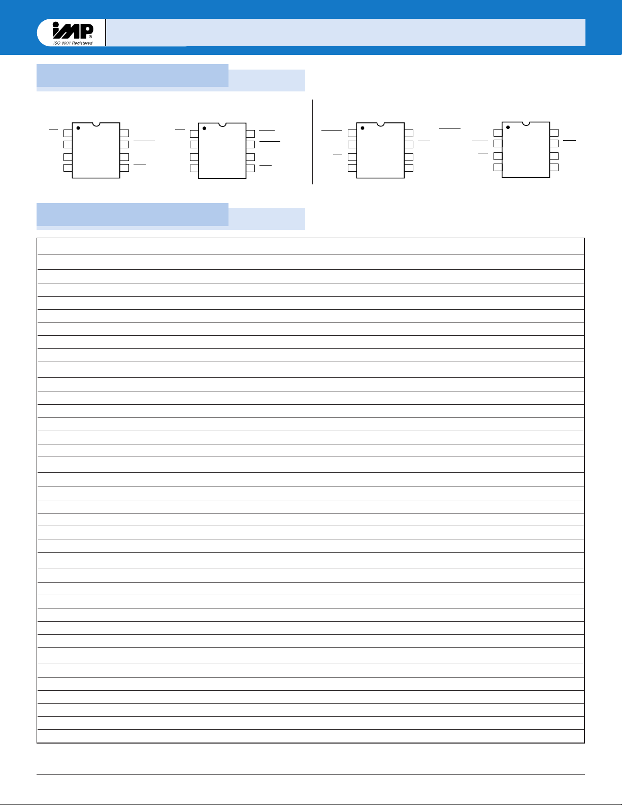
Ordering Information
Pin Configuration
IMP707
IMP708
1
2
3
4
MR
V
CC
GND
PFI
RESET
RESET
NC
PFO
8
7
6
5
IMP707
IMP708
1
2
3
4
RESET
RESET
MR
V
CC
NC
PFO
PFI
GND
8
7
6
5
1
2
3
4
MR
V
CC
GND
PFI
WDO
RESET (RESET)
WDI
PFO
8
7
6
5
IMP705
IMP706
(IMP813L)
IMP705
IMP706
(IMP813L)
1
2
3
4
RESET (RESET)
WDO
MR
V
CC
WDI
PFO
PFI
GND
8
7
6
5
705_03.eps
DIP/SO
MicroSO
Part Number Reset Threshold (V) Temperature Range Pins-Package
IMP705 Active LOW Reset, Watchdog Output and Manual RESET
IMP705CPA 4.65 0°C to +70°C 8-Plastic DIP
IMP705CSA 4.65 0°C to +70°C 8-SO
IMP705CUA 4.65 0°C to +70°C 8-MicroSO
IMP705C/D 4.65 25°C Dice
IMP705EPA 4.65 –40°C to +85°C 8-Plastic DIP
IMP705ESA 4.65 –40°C to +85°C 8-SO
IMP706ESA 4.40 –40°C to +85°C 8-SO
IMP706 Active LOW Reset, Watchdog Output and Manual RESET
IMP706CPA 4.40 0°C to +70°C 8-Plastic DIP
IMP706CSA 4.40 0°C to +70°C 8-SO
IMP706CUA 4.40 0°C to +70°C 8-MicroSO
IMP706C/D 4.40 25°C Dice
IMP706EPA 4.40 –40°C to +85°C 8-Plastic DIP
IMP706ESA 4.40 –40°C to +85°C 8-SO
IMP707 Active LOW & HIGH Reset with Manual RESET
IMP707CPA 4.65 0°C to +70°C 8-Plastic DIP
IMP707CSA 4.65 0°C to +70°C 8-SO
IMP707CUA 4.65 0°C to +70°C 8-MicroSO
IMP707C/D 4.65 25°C Dice
IMP707EPA 4.65 –40°C to +85°C 8-Plastic DIP
IMP707ESA 4.65 –40°C to +85°C 8-SO
IMP708 Active LOW & HIGH Reset with Manual RESET
IMP708CPA 4.40 0°C to +70°C 8-Plastic DIP
IMP708CSA 4.40 0°C to +70°C 8-SO
IMP708CUA 4.40 0°C to +70°C 8-MicroSO
IMP708C/D 4.40 25°C Dice
IMP708EPA 4.40 –40°C to +85°C 8-Plastic DIP
IMP708ESA 4.40 –40°C to +85°C 8-SO
IMP813L Active HIGH Reset, Watchdog Output and Manual RESET
IMP813LCPA 4.65 0°C to +70°C 8-Plastic DIP
IMP813LCSA 4.65 0°C to +70°C 8-SO
IMP813LCUA 4.65 0°C to +70°C 8-MicroSO
IMP813LC/D 4.65 25°C Dice
IMP813LEPA 4.65 –40°C to +85°C 8-Plastic DIP
IMP813LESA 4.65 –40°C to +85°C 8-SO
Page 3
©
1999 IMP, Inc. 408-432-9100/www.impweb.com 3
IMP705/6/7/8, 8
IMP705/6/7/8, 811
3L
3L
Electrical Characteristics
Absolute Maximum Ratings
Pin Terminal Voltage with Respect to Ground
V
CC
. . . . . . . . . . . . . . . . . . . . . . . . . . . . . . . . . –0.3V to 6.0V
All other inputs
1
. . . . . . . . . . . . . . . . . . . . . . . . –0.3V to (VCC+ 0.3V)
Input Current at V
CC
and GND . . . . . . . . . . 20mA
Output Current: All outputs . . . . . . . . . . . . . 20mA
Rate of Rise at V
CC
. . . . . . . . . . . . . . . . . . . . . 100V/µs
Plastic DIP Power Dissipation . . . . . . . . . . . 700 mW
(Derate 9 mW/°C above 70°C)
SO Power Dissipation . . . . . . . . . . . . . . . . . 470 mW
(Derate 5.9 mW/°C above 70°C)
MicroSO Power Dissipation . . . . . . . . . . . . . 330mW
(Derate 4.1 mW/°C above 70°C)
Operating Temperature Range
IMP705E/706E/707E/708E/813LE . . . . . . . – 40°C to 85°C
IMP706C/707C/708C/813LC . . . . . . . . . . . 0°C to 70°C
Storage Temperature Range . . . . . . . . . . . . . . –65°C to 160°C
Lead Temperature Soldering(10 sec) . . . . . . 300°C
Note: 1. The input voltage limits on PFI and MR can be exceeded if
the input current is less than 10mA.
These are stress ratings only and functional operation is not implied.
Parameter Symbol Conditions Min Typ Max Units
Operating Voltage Range V
CC
IMP705/6/7/8C 1.2 5.5 V
IMP813L 1.1 5.5
IMP705/6/7/8E, IMP813lE 1.2 5.5
Supply Current I
CC
IMP705C/706C/813LC 75 140 µA
IMP705E, IMP706E, IMP813LE 75 140
IMP707C, IMP708C 50 140
IMP707E, IMP708E 50 140
RESET Threshold V
RT
IMP705, IMP707, IMP813L, Note 2 4.50 4.65 4.75 V
IMP706, IMP708, Note 2 4.25 4.40 4.50
RESET Threshold Hysteresis Note 2 40 mV
RESET Pulse Width t
RS
Note 2 140 200 280 ms
MR Pulse Width t
MR
0.15 µs
MR to RESET Out Delay t
MD
Note 2 0.25 µs
MR Input Threshold V
IH
2.0 V
V
IL
0.8
MR Pull-up Current MR = 0V 100 250 600 µA
RESET Output Voltage I
SOURCE
= 800µAV
CC
- 1.5V V
I
SINK
= 3.2mA 0.4
IMP705/6/7/8, VCC= 1.2V, I
SINK
= 100µA 0.3
RESET Output Voltage IMP707/708/813L, I
SOURCE
= 800µAV
CC
- 1.5V V
IMP707/708, I
SINK
= 1.2mA 0.4
IMP813L, I
SINK
= 3.2mA 0.4
IMP813L, VCC=1.2V, I
SOURCE
= 4µA 0.9
Watchdog Timeout Period t
WD
IMP705/706/813L 1.00 1.60 2.25 s
WDI Pulse Width t
WP
VIL= 0.4V, VIH= 0.8V
CC
50 ns
WDI Input Threshold V
IH
IMP705/706/813L, VCC= 5V 3.5 V
V
IL
0.8
WDI Input Current IMP705/706/813L, WDI = V
CC
50 150 µA
IMP705/706/813L, WDI = 0V –150 – 50
WDO Output Voltage IMP705/706/813L, I
SOURCE
= 800µAV
CC
- 1.5V V
IMP705/706/813L, I
SINK
= 1.2mA 0.4
PFI Input Threshold VCC= 5V 1.2 1.25 1.3 V
PFI Input Current –25 0.01 25 nA
PFO Output Voltage I
SOURCE
= 800µAV
CC
- 1.5V V
I
SINK
= 3.2mA 0.4
Unless otherwise noted, VCC= 4.75V to 5.5V for the IMP705/707/813L. VCC= 4.5V to 5.5V for the IMP706/708 and over the
operating temperature range.
Notes: 2. RESET (IMP705/6/7/8), RESET (IMP707/8, IMP813L)
Page 4

4
408-432-9100/www.impweb.com
©
1999 IMP, Inc.
IMP705/6/7/8, 8
IMP705/6/7/8, 811
3L
3L
Pin Descriptions
Feature Summary
Pin Number
IMP705/706 IMP707/708 IMP813L
DIP/SO MicroSO DIP/SO MicroSO DIP/SO MicroSO Name Function
Manual RESET input. The active LOW input triggers a reset
1 3 1 3 1 3 MR pulse. A 250µA pull-up current allows the pin to be driven
by TTL / CMOS logic or shorted to ground with a switch.
242424VCC+5V power supply input.
3 5 3 5 3 5 GND Ground reference for all signals.
Power-fail voltage monitor input. With PFI less than
4 6 4 6 4 6 PFI 1.25V, PFO goes low. Connect PFI to ground or V
CC
when not used.
5 7 5 7 5 7 PFO Power-fail output. The output is active LOW and sinks
current when PFI is less than 1.25V.
Watchdog input. WDI controls the internal watchdog
timer. A HIGH or LOW signal for 1.6sec at WDI
allows the internal timer to run-out, setting WDO LOW.
68—— 6 8 WDI The watchdog function is disabled by floating WDI or
by connecting WDI to a high-impedance three-state
buffer. The internal watchdog timer clears when:
RESET is asserted; WDI is three-stated; or WDI sees
a rising or falling edge.
—— 6 ———NC Not connected.
Active-LOW reset output. Pulses LOW for 200ms
when triggered, and stays low whenever V
CC
is below
the reset threshold (IMP705: 4.65V, IMP705J: 4.00V,
7171——RESET IMP706: 4.40V). RESET remains LOW for 200ms
after V
CC
rises above the RESET threshold or MR
goes from LOW to HIGH. A watchdog timeout will not
trigger RESET unless WDO is connected to MR.
Watchdog output. WDO pulls LOW when the 1.6 sec
internal watchdog timer times-out and does not go
HIGH until the watchdog is cleared. In addition, when
82—— 8 2 WDO V
CC
is below the reset threshold, WDO remains low.
Unlike RESET, WDO does not have a minimum pulse
width and as soon as V
CC
exceeds the reset
threshold, WDO goes HIGH with no delay.
—— 8 2 7 1 RESET Active-HIGH reset output. RESET is the inverse of
RESET. The IMP813L has only a RESET output.
IMP705 IMP706 IMP707 IMP708 IMP813L
Power-fail detector ■■■■■
Brownout detection ■■■■■
Manual RESET input ■■■■■
Power-up/down RESET ■■■■■
Watchdog timer ■■ ■
Active-HIGH RESET output ■■■
Active-LOW RESET output ■■ ■ ■
RESET threshold 4.65V/4.00V 4.40V 4.65V 4.40V 4.65V
Page 5
©
1999 IMP, Inc. 408-432-9100/www.impweb.com 5
IMP705/6/7/8, 8
IMP705/6/7/8, 811
3L
3L
Detail Descriptions
RESET/RESET Operation
The RESET/RESET signals are designed to start a µP/µC in a
known state or return the system to a known state.
The IMP707/708 have two RESET outputs, one active-HIGH
RESET and one active-LOW RESET output. The IMP813L has
only an active-HIGH output. RESET is simply the complement
of RESET.
RESET is guaranteed to be LOW with V
CC
above 1.2V. During a
power-up sequence, RESET remains low until the supply rises
above the threshold level, either 4.65V, 4.40V or 4.00V.. RESET goes
high approximately 200ms after crossing the threshold.
During power-down, RESET goes LOW as V
CC
falls below the
threshold level and is guaranteed to be under 0.4V with V
CC
above 1.2V.
In a brownout situation where V
CC
falls below the threshold
level, RESET pulses low. If a brownout occurs during an alreadyinitiated reset, the pulse will continue for a minimum of 140ms.
Auxiliary Comparator
All devices have an auxiliary comparator with 1.25V trip point
and uncommitted output (PFO) and noninverting input (PFI).
This comparator can be used as a supply voltage monitor with an
external resistor voltage divider. The attenuated voltage at PFI
should be set just below the 1.25 threshold. As the supply level
falls, PFI is reduced causing the PFO output to transit LOW.
Normally PFO interrupts the processor so the system can be shut
down in a controlled manner.
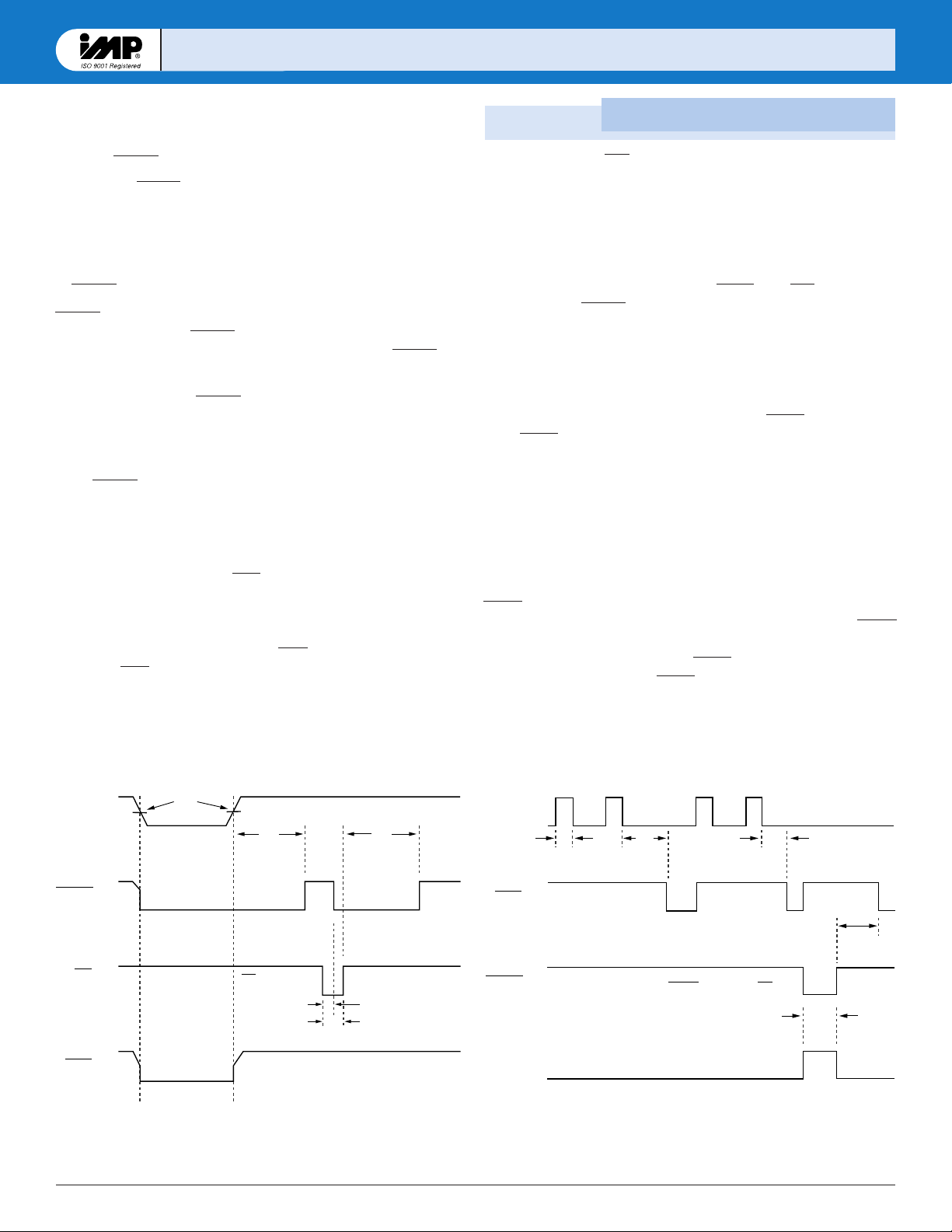
5V
0V
5V
t
WD
t
RS
t
WP
t
WD
t
WD
0V
5V
0V
5V
0V
RESET triggered by MR
WDI
WDO
RESET
IMP813L
(RESET)
705_05.eps
Figure 1. WDI Three-state operation Figure 2. Watchdog Timing
5V
0V
5V
0V
5V
0V
5V
0V
V
CC
v
RT
WDO
RESET
MR
t
MD
t
RS
t
RS
t
MR
MR extermally
set low
705_04.eps
Manual Reset (MR)
The active-LOW manual reset input is pulled high by a 250µA
pull-up current and can be driven low by CMOS/TTL logic or a
mechanical switch to ground. An external debounce circuit is
unnecessary since the 140ms minimum reset time will debounce
mechanical pushbutton switches.
By connecting the watchdog output (WDO) and MR, a watchdog
timeout forces RESET to be generated. The IMP813L should be
used when an active-HIGH RESET is required.
Watchdog Timer
The watchdog timer available on the IMP705/706/813L monitors
µP/µC activity. If activity is not detected within 1.6 seconds, the
internal timer puts the watchdog output, WDO, into a LOW
state. WDO will remain LOW until activity is detected at WDI.
The watchdog function is disabled, meaning it is cleared and not
counting, if WDI is floated or connected to a three-stated circuit.
The watchdog timer is also disabled if RESET is asserted. When
RESET becomes inactive and the WDI input sees a high or low
transition as short as 50ns, the watchdog timer will begin a 1.6
second countdown. Additional transitions at WDI will reset the
watchdog timer and initiate a new countdown sequence.
WDO will also become LOW and remain so, whenever the
supply voltage, V
CC
, falls below the device threshold level. WDO
goes HIGH as soon as V
CC
transitions above the threshold. There
is no minimum pulse width for WDO as there is for the RESET
outputs. If WDI is floated, WDO essentially acts as a low-power
output indicator.
Page 6

6
408-432-9100/www.impweb.com
©
1999 IMP, Inc.
IMP705/6/7/8, 8
IMP705/6/7/8, 811
3L
3L
Application Information
IMP70x
VCC < 1.1V
GND
RESET
100k
W
705_06.eps
V
CC
Ensuring That RESET is Valid Down to VCC= 0V
When VCCfalls below 1.1V, the IMP705-708 RESET output no
longer pulls down; it becomes indeterminate. To avoid the possibility that stray charges build up and force RESET to the wrong
state, a pull-down resistor should be connected to the RESET pin,
thus draining such charges to ground and holding RESET
low. The resistor value is not critical. A 100kΩ resistor will pull
RESET to ground without loading it.
Bi-directional Reset Pin Interfacing
The IMP705/6/7/8 can interface with µP/µC bi-directional reset
pins by connecting a 4.7kΩ resistor in series with the RESET
output and the µP/µC bi-directional RESET pin.
Power
Supply
IMP70x
V
CC
GND GND
RESET
4.7kΩ
705_08.eps
Bi-directional I/O Pin
(Example: 68HC11)
BUF
Buffered
RESET
µC or µP
RESET
Input
Figure 3. Ensuring That RESET is Valid Down to VCC= 0V
Figure 3. Bi-directional Reset Pin Interfacing
Page 7

©
1999 IMP, Inc. 408-432-9100/www.impweb.com 7
IMP705/6/7/8, 8
IMP705/6/7/8, 811
3L
3L
Monitoring Voltages Other Than V
CC
The IMP705-708 can monitor voltages other than VCCusing the
Power Fail circuitry. If a resistive divider is connected from the
voltage to be monitored to the Power Fail input, PFI, the PFO
(output) will go LOW if the divider voltage goes below its 1.25V
reference. Should hysteresis be desired, connect a resistor (equal
to approximately 10 times the sum of the two resistors in the
divider) between the PFI and PFO pins. A capacitor between PFI
and GND will reduce circuit sensitivity to input high-frequency
noise. If it is desired to assert a RESET in addition to the PFO flag,
this may be achieved by connecting the PFO output to MR.
Monitoring a Negative Voltage
The Power-Fail circuitry can also monitor a negative supply rail.
When the negative rail is OK, PFO will be LOW, and when the
negative rail is failing (not negative enough), PFO goes HIGH
(the opposite of when positive voltages are monitored). To trigger
a reset, these outputs need to be inverted: adding the resistors
and transistor as shown achieves this. The RESET output will
then have the same sense as for positive voltages: good = HIGH,
bad = LOW. It should be noted that this circuit’s accuracy depends
on the V
CC
line, the PFI threshold tolerance, and the resistors.
IMP70x
VCC = 5V
VIN = 12V
GND
V
CC
RESET To Processor
12V Threshold
~10.87V
PFO
MR
PFI
1M
W
130k
W
705_07.eps
IMP70x
+
—
+5V
Negative Input
Voltage
GND
V
CC
RESET
PFO
MR
PFI
RP
RN
705_09.eps
5 1 25 1 25−
=
−..RPV
RN
TRIP
Application Information
Figure 4. Monitoring Voltages Other Than V
CC
Figure 5. Monitoring a Negative Voltage
Page 8

IMP705/6/7/8, 8
IMP705/6/7/8, 811
3L
3L
8
408-432-9100/www.impweb.com
©
1999 IMP, Inc.
Plastic DIP (8-Pin)*
L
0°– 8°
C
H
E
e
D
B
A1
A
SO (8-Pin).eps
Inches Millimeters
Min Max Min Max
Plastic DIP (8-Pin)
A ––––– 0.210 –––– 5.33
A1 0.015 ––––– 0.38 –––––
A2 0.115 0.195 2.92 4.95
b 0.014 0.022 0.36 0.56
b2 0.045 0.070 1.14 1.78
b3 0.030 0.045 0.80 1.14
D 0.355 0.400 9.02 10.16
D1 0.005 ––––– 0.13 –––––
E 0.300 0.325 7.62 8.26
E1 0.240 0.280 6.10 7.11
e 0.100 ––––– 2.54
eA 0.300 ––––– 7.62
eB ––––– 0.430 ––––– 10.92
eC ––––– 0.060
L 0.115 0.150 2.92 3.81
MicroSO (8-Pin)
A ––––– 0.0433 –––– 1.10
A1 0.0020 0.0059 0.050 0.15
A2 0.0295 0.0374 0.75 0.95
b 0.0098 0.0157 0.25 0.40
C 0.0051 0.0091 0.13 0.23
D 0.1142 0.1220 2.90 3.10
e 0.0256 BSC 0.65 BSC
E 0.193 BSC 4.90 BSC
E1 0.1142 0.1220 2.90 3.10
L 0.0157 0.0276 0.40 0.70
a0° 6° 0° 6°
SO (8-Pin)
A 0.053 0.069 1.35 1.75
A1 0.004 0.010 0.10 0.25
B 0.013 0.020 0.33 0.51
C 0.007 0.010 0.19 0.25
e 0.050 1.27
E 0.150 0.157 3.80 4.00
H 0.228 0.244 5.80 6.20
L 0.016 0.050 0.40 1.27
D 0.189 0.197 4.80 5.00
SO (8-Pin)***
MicroSO (8-Pin)**
e
b
D
E1 E
a
L
+
C
D
0.10mm
0.004in
A1
A2
A
MicroSO (8-Pin).eps
* JEDEC Drawing MS-001BA
** JEDEC Drawing MO-187AA
*** JEDEC Drawing MS-012AA
Package Dimensions
D1
D
A2
A
E
E1
L
A1
e
b2
b
0°–15°
C
eA
eB
Plastic DIP (8-Pin)a.eps
Page 9

IMP705/6/7/8, 8
IMP705/6/7/8, 811
3L
3L
IMP, Inc.
Corporate Headquarters
2830 N. First Street
San Jose, CA 95134-2071
Tel: 408-432-9100
Tel: 800-438-3722
Fax: 408-434-0335
e-mail: info@impinc.com
http://www.impweb.com
The IMP logo is a registered trademark of IMP, Inc.
All other company and product names are trademarks of their respective owners.
© 1999 IMP, Inc.
Printed in USA
Publication #: 1017
Revision: A
Issue Date: 08/17/99
Type: Preliminary
 Loading...