

Page 1
©
1999 IMP, Inc. 408-432-9100/www.impweb.com 1
Key Features
Applications
◆ Embedded control systems
◆ Battery–operated systems
◆ Intelligent instruments
◆ Wireless communication systems
◆ PDAs and handheld equipment
◆ µP/µC power supply monitoring
◆
Design improvement over Maxim
MAX690A/692A/802L/802M/805L
— 70% lower current than Maxim:
100µA maximum
— RESET Operation to 1.1V
◆
Two precision supply-voltage monitor options
— 4.65V (IMP690A/802L/805L)
— 4.40V (IMP692A/802M)
◆
Battery-backup power switch on-chip
◆
Watchdog timer: 1.6 second timeout
◆
Power failure/low battery detection
◆
Short-circuit protection and thermal limiting
◆
Small 8-pin SO package
◆
No external components
◆
Specified over full temperature range
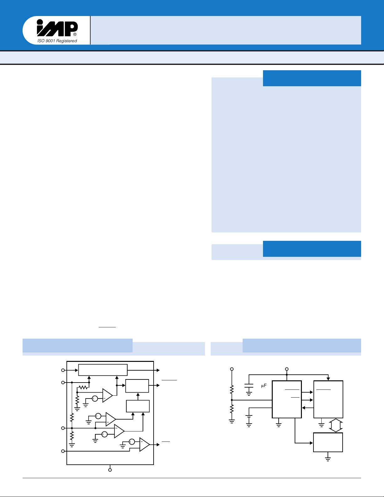
Block Diagrams
IMP690A
IMP690A
, 692A
, 692A
, 802L/M, 805L
, 802L/M, 805L
POWER MANAGEMENT
µµP Super
P Super
visor wit
visor wit
h Batt
h Battereryy
Bac
Bac
kup Switc
kup Switchh
The IMP690A/IMP692A/IMP802L/IMP802M/IMP805L simplify power
supply monitoring and control in microprocessor systems. Each circuit
implements four functions: Reset control, watchdog monitoring, batterybackup switching and power-failure monitoring. In addition to
microprocessor reset under powerup and power-down conditions, these
devices provide battery-backup switching to maintain control in powerloss and brown-out situations. Additional monitoring capabilities
can provide an early warning of unregulated power-supply loss before
the voltage regulator drops out. The important features of these four
functions are:
a) 1.6 second watchdog timer to keep microprocessor responsive
b) 4.40V or 4.65V V
CC
threshold for microprocessor reset at power-up
and power-down
c) SPDT (single-pole, double-throw) PMOS switch connects backup
power to RAM if V
CC
fails
d) 1.25V threshold detector for power loss or general purpose voltage
monitoring
While these features are pin–compatible with the industry standard
power–supply supervisors offered by Maxim, the IMP devices are superior replacements and can reduce power requirements by 70 percent
when compared to Maxim MAX690/MAX692A/MAX802L/MAX802M/
MAX805L devices. Short-circuit and thermal protection have also
been added.
The IMP690A/IMP802L/IMP805L generate a reset pulse when the
supply voltage drops below 4.65V, and the IMP692A/IMP802M
generate a reset below 4.40V. The IMP802L/IMP802M have power–fail
accuracy to ±2%. The IMP805L is the same as the IMP690A except that
RESET is provided instead of RESET.
+
+
+
+
+
+
+
+
V
CC
V
OUT
1
7
5
3
PFI
WDI
GND
V
BATT
8
2
6
4
PFO
IMP690A, IMP692A, IMP802L, IMP802M,
IMP805L
RESET
(RESET)
( ) IMP805L
Battery-Switchover
Circuit
Reset
Generator
Watchdog
Timer
3.5V
1.25V
1.25V
0.8V
690A_03.eps
Typical Application
Unregulated DC Regulated +5V
R
R
0.1mF
1
2
3.6V
+
Lithium
–
Battery
V
CC
RESET
PFO
PFI
V
WDI
BATT
V
OUT
GND
IMP690A
V
RESET
NMI
I/O LINE
GND
CMOS
RAM
V
CC
GND
CC
BUS
690A_01.eps
Page 2
2
408-432-9100/www.impweb.com
©
1999 IMP, Inc.
Ordering Information
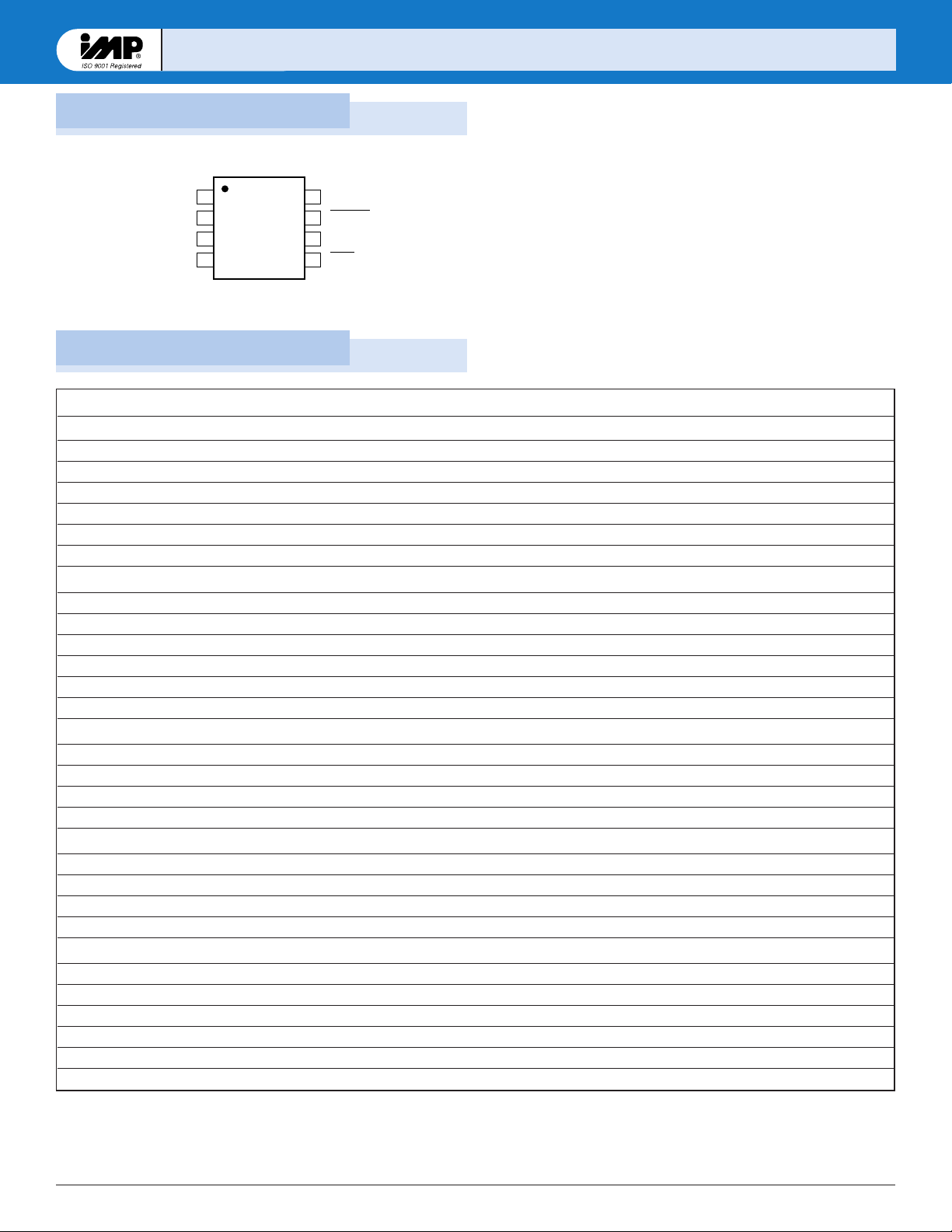
Pin Configuration
IMP690A
IMP690A
, 692A
, 692A
, 802L, 802M, 805L
, 802L, 802M, 805L
4PFI
3GND
2V
CC
1V
OUT
5 PFO
6 WDI
7 RESET (RESET)
8V
BATT
690A_02.eps
IMP690A
IMP692A
IMP802L
IMP802M
IMP805L
( ) IMP805L
Plastic/CerDip/SO
Part Number Reset Threshold (V) Temperature Range Pins-Package
IMP690A
IMP690ACPA 4.5 to 4.75 0°C to +70°C 8-Plastic DIP
IMP690ACSA 4.5 to 4.75 0°C to +70°C 8-SO
IMP690AC/D 4.5 to 4.75 25°C DICE
IMP690AEPA 4.5 to 4.75 –40°C to +85°C 8-Plastic DIP
IMP690AESA 4.5 to 4.75 –40°C to +85°C 8-SO
IMP690AMJA 4.5 to 4.75 Contact Factory 8-CerDIP
IMP692A
IMP692ACPA 4.25 to 4.50 0°C to +70°C 8-Plastic DIP
IMP692ACSA 4.25 to 4.50 0°C to +70°C 8-SO
IMP692AC/D 4.25 to 4.50 25°C DICE
IMP692AEPA 4.25 to 4.50 – 40°C to +85°C 8-Plastic DIP
IMP692AESA 4.25 to 4.50 – 40°C to +85°C 8-SO
IMP692AMJA 4.25 to 4.50 Contact Factory 8-CerDIP
IMP802L
IMP802LCPA 4.5 to 4.75 0°C to +70°C 8-Plastic DIP
IMP802LCSA 4.5 to 4.75 0°C to +70°C 8-SO
IMP802LEPA 4.5 to 4.75 –40°C to +85°C 8-Plastic DIP
IMP802LESA 4.5 to 4.75 –40°C to +85°C 8-SO
IMP802M
IMP802MCPA 4.25 to 4.50 0°C to +70°C 8-Plastic DIP
IMP802MCSA 4.25 to 4.50 0°C to +70°C 8-SO
IMP802MEPA 4.25 to 4.50 –40°C to +85°C 8-Plastic DIP
IMP802MESA 4.25 to 4.50 –40°C to +85°C 8-SO
IMP805L
IMP805LCPA 4.5 to 4.75 0°C to +70°C 8-Plastic DIP
IMP805LCSA 4.5 to 4.75 0°C to +70°C 8-SO
IMP805LC/D 4.5 to 4.75 25°C DICE
IMP805LEPA 4.5 to 4.75 –40°C to +85°C 8-Plastic DIP
IMP805LESA 4.5 to 4.75 –40°C to +85°C 8-SO
IMP805LMJA 4.5 to 4.75 Contact Factory 8-CerDIP
Page 3
©
1999 IMP, Inc. 408-432-9100/www.impweb.com 3
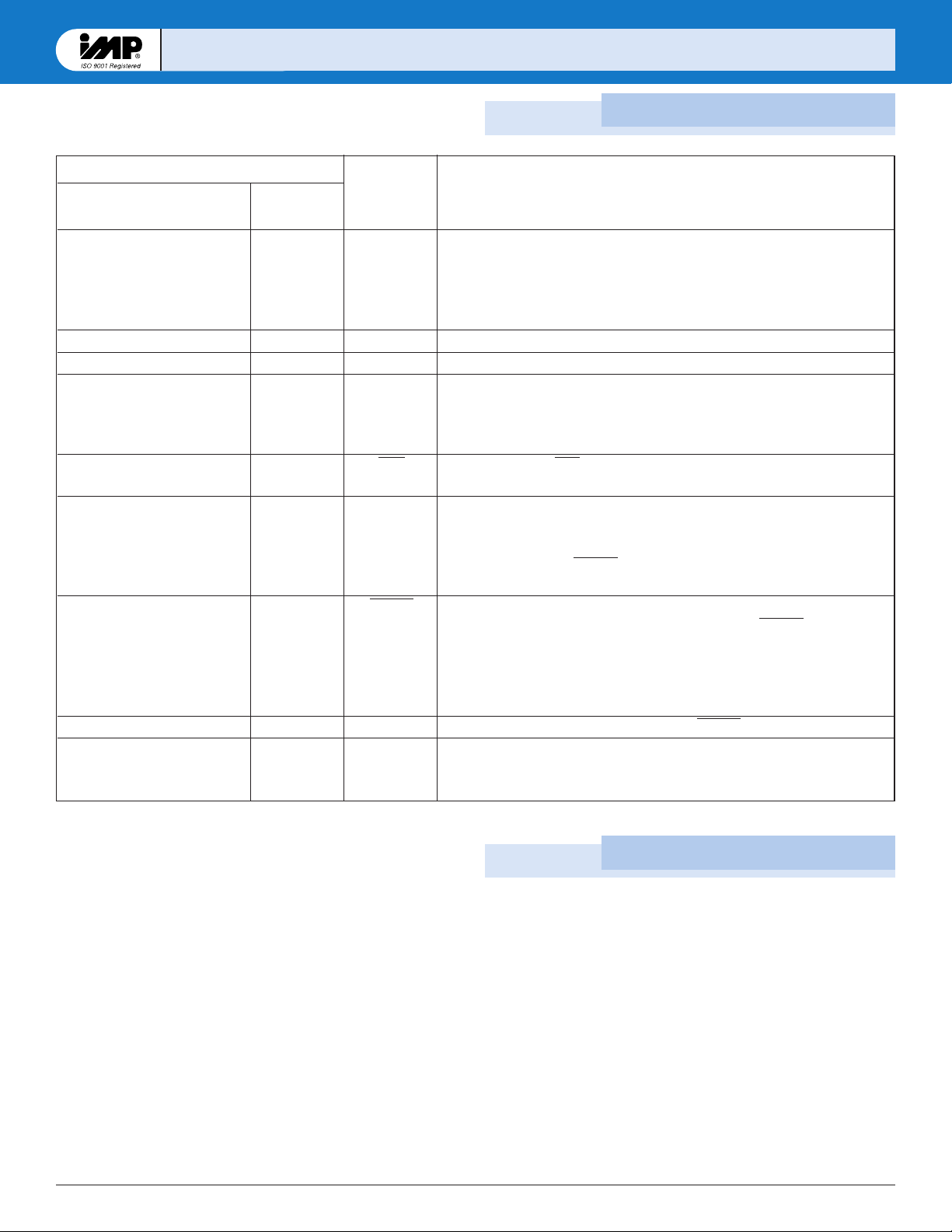
Pin Number
IMP690A/IMP692A
IMP802L/IMP802M IMP805L Name Function
11V
OUT
Voltage supply for RAM. When VCCis above the reset threshold, V
OUT
connects to VCCthrough a P-channel MOS device. If VCCfalls below the
reset threshold, this output will be connected to the backup supply at
V
BATT
(or VCC, whichever is higher) through the MOS switch to provide
continuous power to the CMOS RAM.
22V
CC
+5V power supply input
3 3 GND Ground
4 4 PFI Power failure monitor input. PFI is connected to the internal power fail
comparator which is referenced to 1.25V. The power fail output (PFO)
is active LOW but remains HIGH if PFI is above 1.25V. If this feature is
unused, the PFI pin should be connected to GND or V
OUT
.
5 5 PFO Power-fail output. PFO is active LOW whenever the PFI pin is less than
1.25V.
6 6 WDI Watchdog input. The WDI input monitors microprocessor activity. An
internal timer is reset with each transition of the WDI input. If WDI is held
HIGH or LOW for longer than the watchdog timeout period, typically 1.6
seconds, RESET (or RESET) is asserted for the reset pulse width time,
tRS, of 140ms, minimum.
7 –––– RESET Active-LOW reset output. When triggered by VCCfalling below the reset
threshold or by watchdog timer timeout, RESET (or RESET) pulses low
for the reset pulse width, tRS, typically 200ms. It will remain low if VCCis
below the reset threshold (4.65V in the IMP690A/IMP802L and 4.4V in
the IMP692A/IMP802L) and remains low for 200ms after VCCrise above
the reset threshold.
–––– 7 RESET Active-HIGH reset output. The inverse of RESET.
88V
BATT
Auxiliary power or backup-battery input. V
BATT
should be connected to
GND if the function is not used. This input has about 40mV of hysteresis
to prevent rapid toggling between VCCand V
BATT
.
IMP690A
IMP690A
, 692A
, 692A
, 802L, 802M, 805L
, 802L, 802M, 805L
Absolute Maximum Ratings
Pin Description
Pin Terminal Voltage with Respect to Ground
V
CC
. . . . . . . . . . . . . . . . . . . . . . . . . . . . . . –0.3V to 6.0V
V
BATT
. . . . . . . . . . . . . . . . . . . . . . . . . . . . –0.3V to 6.0V
All Other Inputs* . . . . . . . . . . . . . . . . . . . – 0.3V to (V
CC
+ 0.3V)
Input Current at V
CC
. . . . . . . . . . . . . . . . . . 200mA
Input Current at V
BATT
. . . . . . . . . . . . . . . . . 50mA
Input Current at GND . . . . . . . . . . . . . . . . . 20mA
Output Current:
V
OUT
. . . . . . . . . . . . . . . Short circuit protected
All Other Inputs . . . . . . . . . . . . . . . . . . . 20mA
Rate of Rise: V
BATT
and VCC . . . . . . . . . . 100V/µs
Continuous Power Dissipation
Plastic DIP (derate 9mW/°C above 70°C) . . . 800mW
SO (derate 5.9mW/°C above 70°C) . . . . . . . . 500mW
CerDIP (derate 8mW/°C above 70°C) . . . . . . 650mW
Operating Temperature Range (C Devices) . . . . 0°C to 70°C
Operating Temperature Range (E Devices) . . . . – 40°C to 85°C
Storage Temperature Range . . . . . . . . . . . . . . . . . – 65°C to 160°C
Lead Temperature Soldering, (10 sec) . . . . . . . . 300°C
* The input voltage limits on PFI and WDI may be exceeded if the
current is limited to less than 10mA
These are stress ratings only and functional operation is not implied.
Exposure to absolute maximum ratings for prolonged time periods may
affect device reliability.
Page 4
4
408-432-9100/www.impweb.com
©
1999 IMP, Inc.
IMP690A
IMP690A
, 692A
, 692A
, 802L, 802M, 805L
, 802L, 802M, 805L
Electrical Characteristics
Parameter Symbol Conditions Min Typ Max Units
VCC, V
BATT
Voltage Range IMP69_AC, IMP802_C 1.1 5.5 V
(Note 1) IMP805LC 1.1 5.5
IMP69_AE, IMP80_ _E 1.1 5.5
Supply Current Excluding I
OUT
I
S
IMP69_AC, IMP802_C 35 100 µA
IMP69_AE, IMP802_E, IMP805LE 35 100
I
SUPPLY
in Battery-Backup Mode V
CC
= 0V, V
BATT
= 2.8V TA= 25°C 1.0 µA
(Excluding I
OUT
)T
A
= T
MIN
to T
MAX
5.0
V
BATT
Standby Current 5.5V > VCC> V
BATT
– 0.2V TA= 25°C –0.1 0.02 µA
(Note 2) TA= T
MIN
to T
MAX
–1.0 0.02
V
OUT
Output I
OUT
= 5mA VCC– 0.025 VCC– 0.010 V
I
OUT
= 50mA VCC– 0.25 VCC– 0.10
V
OUT
in Battery-Backup Mode I
OUT
= 250µA, VCC< V
BATT
– 0.2V V
BATT
– 0.1 V
BATT
– 0.001 V
Battery Switch Threshold, V
CC
< V
RT
Power-up 20 mV
VCCto V
BATT
Power-down –20
Battery Switchover Hysteresis 40 mV
Reset Threshold V
RT
IMP690A/802L/805L 4.50 4.65 4.75 V
IMP692A, IMP802M 4.25 4.40 4.50
IMP802L, TA= 25°C, VCCfalling 4.55 4.70
IMP802M, TA= 25°C, VCCfalling 4.30 4.45
Reset Threshold Hysteresis 40 mV
Reset Pulse Width t
RS
140 200 280 ms
Reset Output Voltage I
SOURCE
= 800µA V
CC
– 1.5 V
I
SINK
= 3.2mA 0.4
IMP69_AC, IMP802_C, VCC= 1.0V, I
SINK
= 50µA 0.3
IMP69_AE, IMP802_E, VCC= 1.2V, I
SINK
= 100µA 0.3
IMP805LC, I
SOURCE
= 4µA, V
CC
= 1.1V 0.8
IMP805LE, I
SOURCE
= 4µA, V
CC
= 1.2V 0.9
IMP805L, I
SOURCE
= 800µAV
CC
– 1.5
IMP805L, I
SINK
= 3.2mA 0.4
Watchdog Timeout t
WD
1.00 1.60 2.25 sec
WDI Pulse Width t
WP
VIL= 0.4V, V
IH
= 0.8V
CC
50 ns
WDI Input Current WDI = V
CC
50 150 µA
WDI = 0V –150 –50
WDI Input Threshold VCC= 5V, Logic LOW 0.8 V
(Note 3) VCC= 5V, Logic HIGH 3.5
PFI Input Threshold IMP69_A, IMP805L, VCC= 5V 1.20 1.25 1.30 V
IMP802_C/E, VCC= 5V 1.225 1.250 1.275
PFI Input Current –25 0.01 25 nA
PFO Output Voltage I
SOURCE
= 800µA VCC– 1.5 V
I
SINK
= 3.2mA 0.4
Unless otherwise noted VCC= 4.75V to 5.5V for the IMP690A/IMP802L/IMP805L and VCC= 4.5V to 5.5V for the IMP692A/IMP802M;
V
BATT
= 2.8V; and TA= T
MIN
to T
MAX
.
Notes: 1. If VCCor V
BATT
is 0V, the other must be greater than 2.0V.
2. Battery charging-current is “–”. Battery discharge-current is “+”.
3. WDI is guaranteed to be in an intermediate level state if WDI is floating and V
CC
is within the operating voltage range. WDI input
impedance is 50kΩ. WDI is biased to 0.3V
CC
.
Page 5

©
1999 IMP, Inc. 408-432-9100/www.impweb.com 5
IMP690A
IMP690A
, 692A
, 692A
, 802L, 802M, 805L
, 802L, 802M, 805L
Application Information
Reset Output
It is important to initialize a microprocessor to a known state in
response to specific events that could create code execution errors
and “lock-up”. The reset output of these supervisory circuits send
a reset pulse to the microprocessor in response to power-up,
power-down/power-loss or a watchdog time-out. The reset pulse
width, t
RS
, is typically around 200ms and is LOW for the
IMP690A, IMP692A, IMP802 and HIGH for the IMP805L.
Power-up reset occurs when a rising V
CC
reaches the reset thresh-
old, V
RT
, forcing a reset condition in which the reset output is
asserted in the appropriate logic state for the duration of t
RS
.
Figure 2 shows the reset pin timing.
Power-loss or “brown-out” reset occurs when V
CC
dips below the
reset threshold resulting in a reset assertion for the duration of t
RS
.
The reset signal remains asserted as long as VCCis between V
RT
and 1.1V, the lowest VCCfor which these devices can provide a
guaranteed logic-low output. To ensure logic inputs connected to
the IMP690A/692A/802 RESET pin are in a known state when
V
CC
is under 1.1V, a 100kΩ pull-down resistor at RESET is needed:
the logic-high IMP805L will need a pull-up resistor to V
CC
.
A Watchdog time-out reset occurs when a logic “1” or logic “0” is
continuously applied to the WDI pin for more than 1.6 seconds.
After the duration of the reset interval, the watchdog timer starts
a new 1.6 second timing interval; the microprocessor must service
the watchdog input by changing states or by floating the WDI pin
before this interval is finished. If the WDI pin is held either HIGH
or LOW, a reset pulse will be triggered every 1.8 seconds (the 1.6
second timing interval plus the reset pulse width t
RS
).
+
+
+
+
+
+
+
+
V
CC
V
OUT
1
7
5
3
PFI
WDI
GND
V
BATT
8
2
6
4
PFO
IMP690A, IMP692A, IMP802L, IMP802M,
IMP805L
RESET
(RESET)
( ) IMP805L
Battery-Switchover
Circuit
Reset
Generator
Watchdog
Timer
3.5V
1.25V
1.25V
0.8V
690A_03.eps
Figure 1. Block Diagram
V
CC
V
OUT
V
BATT
= PFI = 3.0V
I
OUT
= 0mA
PFO
+5V
+5V
+0V
+0V
3.0V
+5V
+0V
+5V
+0V
+5V
+0V
( ) IMP805L
3.0V
RESET
(RESET)
690A_04.eps
t
RS
Figure 2. Timing Diagram
Page 6

6
408-432-9100/www.impweb.com
©
1999 IMP, Inc.
IMP690A
IMP690A
, 692A
, 692A
, 802L, 802M, 805L
, 802L, 802M, 805L
Application Information
Microprocessor Interface.
The IMP690 has logic-LOW RESET output while the IMP805 has
an inverted logic-HIGH RESET output. Microprocessors with bidirectional reset pins (69HC11 for example) can pose a problem
when the supervisory circuit and the microprocessor output pins
attempt to go to opposite logic states. The problem can be
resolved by placing a 4.7kΩ resistor between the RESET output
and the microprocessor reset pin. This is shown in Figure 3. Since
the series resistor limits drive capabilities, the reset signal to other
devices should be buffered.
Figure 3. Interfacing with bi-directional microprocessor
reset inputs
Watchdog Input
As discussed in the Reset section, the Watchdog Input is used to
monitor microprocessor activity. It can be used to insure that the
microprocessor is in a continually responsive state by requiring
that the WDI pin be toggled every second. If the WDI pin is not
toggled within the 1.6 second window (minimum t
WD
+ tRS),
a reset pulse will be asserted to return the microprocessor to the
initial start-up state. Pulses as short as 50ns can be applied to the
WDI pin. If this feature is not used, the WDI pin should be opencircuited or the logic placed into a high-impedance state to allow
the pin to float.
690A_05.eps
GND GND
RESETRESET
V
CC
IMP690A
V
CC
4.7k
Buffered RESET to Other System Components
Backup-Battery Switchover
A power loss can be made less severe if the system RAM contents
are preserved. This is achieved in the IMP690/692/802/805 by
switching from the failed V
CC
to an alternate power source con-
nected at V
BATT
when VCCis less than the reset threshold voltage
(V
CC
< VRT), and VCCis less than V
BATT
. The V
OUT
pin is normally
connected to V
CC
through a 2Ω PMOS switch but a brown-out or
loss of V
CC
will cause a switchover to V
BATT
by means of a 20Ω
PMOS switch. Although both conditions (V
CC
< VRTand VCC<
V
BATT
) must occur for the switchover to V
BATT
to occur, V
OUT
will
be switched back to V
CC
when VCCexceeds VRTirrespective of the
voltage at V
BATT
. It should be noted that an internal device diode
(D1 in Figure 4) will be forward biased if V
BATT
exceeds VCCby
more than a diode drop when V
CC
is switched to V
OUT
. Because of
this it is recommended that V
BATT
be no greater than V
RT
+0.6V.
Figure 4. Internal device configuration of battery
switch-over function
V
CC
> Reset Threshold
V
CC
< Reset Threshold and
V
CC
> V
BATT
V
CC
< Reset Threshold and
V
CC
< V
BATT
IMP690A/IMP802L / IMP805L Reset Threshold = 4.65V
IMP692A/IMP802M Reset Threshold = 4.4V
Closed
Open
Open
Closed
Closed Open
CONDITION SW1/SW2 SW3/SW4
690A_06.eps
SW4SW3D2D1
D3
IMP690A
IMP692A
IMP802L
IMP802M
IMP805L
SW1 SW2
V
CC
V
OUT
V
BATT
Page 7

©
1999 IMP, Inc. 408-432-9100/www.impweb.com 7
IMP690A
IMP690A
, 692A
, 692A
, 802L, 802M, 805L
, 802L, 802M, 805L
Application Information
Table 1. Pin Connections in Battery Backup Mode
During the backup power mode, the internal circuitry of the
supervisory circuit draws power from the battery supply. While
V
CC
is still alive, the comparator circuits remain alive and the cur-
rent drawn by the device is typically 35µA. When V
CC
drops more
than 1.1V below V
BATT
, the internal switchover comparator, the
PFI comparator and WDI comparator will shut off, reducing the
quiescent current drawn by the IC to less than 1µA.
Backup Power Sources - Batteries
Battery voltage selection is important to insure that the battery
does not discharge through the parasitic device diode D1 (see
Figure 4) when V
CC
is less than V
BATT
and VCC> VRT.
Table 2. Maximum Battery Voltages
Although most batteries that meet the requirements of Table 2 are
acceptable, lithium batteries are very effective backup source due
to their high-energy density and very low self-discharge rates.
Battery Replacement while Powered
Batteries can be replaced even when the device is in a powered
state as long as V
CC
remains above the reset threshold voltage VRT.
In the IMP devices, a floating V
BATT
pin will not cause a powersupply switchover as can occur in some other supervisory
circuits. If V
BATT
is not used, the pin should be grounded.
Part No. MAXIMUM Battery Voltage
IMP690A 4.80
IMP802L 4.80
IMP805L 4.80
IMP692A 4.55
IMP802M 4.55
Pin Connection
V
OUT
Connected to V
BATT
through internal PMOS switch
V
BATT
Connected to V
OUT
PFI Disabled
PFO Logic-LOW
RESET Logic LOW (except on IMP805 where it is HIGH)
WDI Watchdog timer disabled
Backup Power Sources - SuperCap
TM
Capacitor storage, with very high values of capacitance, can be
used as a back-up power source instead of batteries. SuperCap
TM
are capacitors with capacities in the fractional farad range. A 0.1
farad SuperCap
TM
would provide a useful backup power source.
Like the battery supply, it is important that the capacitor voltage
remain below the maximum voltages shown in Table 2. Although
the circuit of Figure 5 shows the most simple way to connect the
SuperCap
TM
, this circuit cannot insure that an overvoltage condition will not occur since the capacitor will ultimately charge up to
V
CC
. To insure that an overvoltage condition does not occur,
the circuit of Figure 6 is preferred. In this circuit configuration, the
diode-resistor pair clamps the capacitor voltage at one diodedrop below V
CC
. VCCitself should be regulated within ±5% of
5V for the IMP692A/802M or within ±10% of 5V for the
IMP690A/802L/805L to insure that the storage capacitor does not
achieve an overvoltage state.
Note: SuperCap
TM
is a trademark of Baknor Industries
Figure 5. Capacitor as a backup power source
Figure 6. Capacitor as back-up Power Source - Voltage
clamped to 0.5V below V
CC
690A_08.eps
+5V
GND
IMP692A
IMP802M
( ) IMP805L
100k
+
0.1F
V
BATT
V
CC
To mP
To Static RAM
RESET
V
OUT
+
690A_07.eps
+5V
GND
( ) IMP805L
0.1F
V
BATT
V
CC
To mP
To Static RAM
RESET
(RESET)
V
OUT
Page 8

8
408-432-9100/www.impweb.com
©
1999 IMP, Inc.
IMP690A
IMP690A
, 692A
, 692A
, 802L, 802M, 805L
, 802L, 802M, 805L
Application Information
Operation Without a Backup Power Source
When operating without a back-up power source, the V
BATT
pin
should be connected to GND and V
OUT
should be connected to
V
CC
, since power source switchover will not occur. Connecting
V
OUT
to VCCeliminates the voltage drop due to the ON-resistance
of the PMOS switch.
Power-Fail Comparator
The Power Fail feature is an independent voltage monitoring
function that can be used for any number of monitoring activities.
The PFI function can provide an early sensing of power supply
failure by sensing the voltage of the unregulated DC ahead of
the regulated supply sensing seen by the backup-battery
switchover circuitry.
The PFI pin is compared to a 1.25V internal reference. If the voltage at the PFI pin is less than this reference voltage, the PFO pin
goes low. By sensing the voltage of the raw DC power supply, the
microprocessor system can prepare for imminent power-loss,
especially if the battery backup supply is not enabled. The input
voltage at the PFI pin results from a simple resistor voltage
divider as shown in Figure 7.
Figure 7. Simple Voltage divider sets PFI trip point
690A_09.eps
+5V
GND
0V
PFO
+5V
A
AB
B
IMP690A
IMP692A
IMP802L
IMP802M
IMP805L
R
2
PFI
V
CC
PFO
R
1
Power Fail Hysteresis
A noise margin can be added to the simple monitoring circuit of
Figure 7 by adding positive feedback from the PFO pin. The circuit
of Figure 8 adds this positive “latching” effect by means of an
additional resistor R3 connected between PFO and PFI which
helps in pulling PFI in the direction of PFO and eliminating an
indecision at the trip point. Resistor R3 is normally about 10 times
higher in resistance than R2 to keep the hysteresis band reasonable and should be larger than 10kΩ to avoid excessive loading on
the PFO pin. The calculations for the correct values of resistors to
set the hysteresis thresholds are given in Figure 8. A capacitor can
be added to offer additional noise rejection by low-pass filtering.
Figure 8. Hysteresis added to PFI pin
690A_10.eps
V
TRIP
V
L
V
H
V
IN
0V
PFO
+5V
0V
V
IN
GND
IMP690A
IMP692A
IMP802L
IMP802M
IMP805L
R
2
PFI
V
CC
R
1
PFO
+5V
R
3
To mP
*Optional
C1*
5
125
2
12
R
RR
V
+
< .
5
125
2
12
R
RR
V
+
> .
V
R
RR
V
RR
RRR
V
RRR
TRIP
IH
L
=
+
=
+
−
+
−
=
125
125
125 5 125 125
2
22
23
123
132
.
.
...
Page 9

©
1999 IMP, Inc. 408-432-9100/www.impweb.com 9
IMP690A
IMP690A
, 692A
, 692A
, 802L, 802M, 805L
, 802L, 802M, 805L
Application Information
Monitoring Capabilities of the Power-Fail Input
Although designed for power supply failure monitoring, the PFI
pin can be used for monitoring any voltage condition that can be
scaled by means of a resistive divider. An example is the negative
power supply monitor configured in Figure 9. In this case a good
negative supply will hold the PFI pin below 1.25V and the PFO
pin will be at a logic “0”. As the negative voltage declines,
the voltage at the PFI pin will rise until it exceeds 1.25V and
the PFO pin will go to a logic “1”.
Figure 9. Using PFI to monitor negative supply voltage
5 1 25 1 25
12
−
=
−..RV
R
TRIP
690A_11.eps
+5V
GND
V
TRIP
0V
PFO
+5V
0V
V–
IMP690A
IMP692A
IMP802L
IMP802M
IMP805L
R
2
V–
PFI
V– = V
TRIP
V
CC
PFO
R
1
Page 10

10
408-432-9100/www.impweb.com
©
1999 IMP, Inc.
IMP690A
IMP690A
, 692A
, 692A
, 802L, 802M, 805L
, 802L, 802M, 805L
IMP690A
IMP690A
, 692A
, 692A
, 802L, 802M, 805L
, 802L, 802M, 805L
Package Dimensions
Plastic DIP (8-Pin)
L
0°– 8°
C
H
E
e
D
B
A1
A
SO (8-Pin).eps
Inches Millimeters
Min Max Min Max
Plastic DIP (8-Pin)*
A ––––– 0.210 –––– 5.33
A1 0.015 ––––– 0.38 –––––
A2 0.115 0.195 2.92 4.95
b 0.014 0.022 0.36 0.56
b2 0.045 0.070 1.14 1.78
b3 0.030 0.045 0.80 1.14
D 0.355 0.400 9.02 10.16
D1 0.005 ––––– 0.13 –––––
E 0.300 0.325 7.62 8.26
E1 0.240 0.280 6.10 7.11
e 0.100 ––––– 2.54
eA 0.300 ––––– 7.62
eB ––––– 0.430 ––––– 10.92
eC ––––– 0.060
L 0.115 0.150 2.92 3.81
CerDIP (8-Pin)
A ––––– 0.200 –––– 5.08
A1 0.015 0.070 0.38 1.78
b 0.014 0.023 0.36 0.58
b2 0.038 0.065 0.97 1.65
C 0.008 0.015 0.20 0.38
D ––––– 0.405 ––––– 10.29
D1 0.005 ––––– 0.13 –––––
E 0.290 0.320 7.37 8.13
E1 0.220 0.310 5.59 7.87
e 0.100 2.54
L 0.125 0.200 3.18 5.08
SO (8-Pin)**
A 0.053 0.069 1.35 1.75
A1 0.004 0.010 0.10 0.25
B 0.013 0.020 0.33 0.51
C 0.007 0.010 0.19 0.25
e 0.050 1.27
E 0.150 0.157 3.80 4.00
H 0.228 0.244 5.80 6.20
L 0.016 0.050 0.40 1.27
D 0.189 0.197 4.80 5.00
SO (8-Pin)
* JEDEC Drawing MS-001BA
** JEDEC Drawing MS-012AA
CerDIP (8-Pin)
D1
D
A2
A
L
A1
e
b2
b
E
E1
0°–15°
C
eA
eB
Plastic DIP (8-Pin)a.eps
D1
D
A
L
A1
e
b2
b
E
E1
0°–15°
C
Ceramic DIP (8-Pin)a.eps
Page 11

IMP690A
IMP690A
, 692A
, 692A
, 802L, 802M, 805L
, 802L, 802M, 805L
IMP, Inc.
Corporate Headquarters
2830 N. First Street
San Jose, CA 95134-2071
Tel: 408-432-9100
Tel: 800-438-3722
Fax: 408-434-0335
e-mail: info@impinc.com
http://www.impweb.com
The IMP logo is a registered trademark of IMP, Inc.
All other company and product names are trademarks of their respective owners.
© 1999 IMP, Inc.
Printed in USA
Publication #: 1016
Revision: A
Issue Date: 08/17/99
Type: Preliminary
 Loading...