

Page 1
© 2000 IMP, Inc. 408-432-9100/www.impweb.com 1
IMP52
IMP5277
POWER MANAGEMENT
Sing
Sing
le Cell Batt
le Cell Batterer
y P
y Poowwerer
ed
ed
Electr
Electr
oluminescent Lam
oluminescent Lampp
Dr
Driviv
er/In
er/Invverertterer
◆ Audio/TV remote control units
◆ Pagers/Cellular phones
◆ PDAs
◆ Clocks and radios
◆ Portable GPS receivers
◆ LCD modules
◆ Toys
◆ Wide operating voltage range - from 0.9V to 2.5V
◆ Simple design requires few passive components
◆ 180V peak-to-peak typical AC output voltage
◆ Adjustable output frequency controls lamp
color and power consumption
◆ Adjustable converter frequency minimizes
circuit power consumption
◆ Disable mode extends battery life
◆ Disable current 1µA typical
◆ Compact MicroSO package option
Key Features
Applications
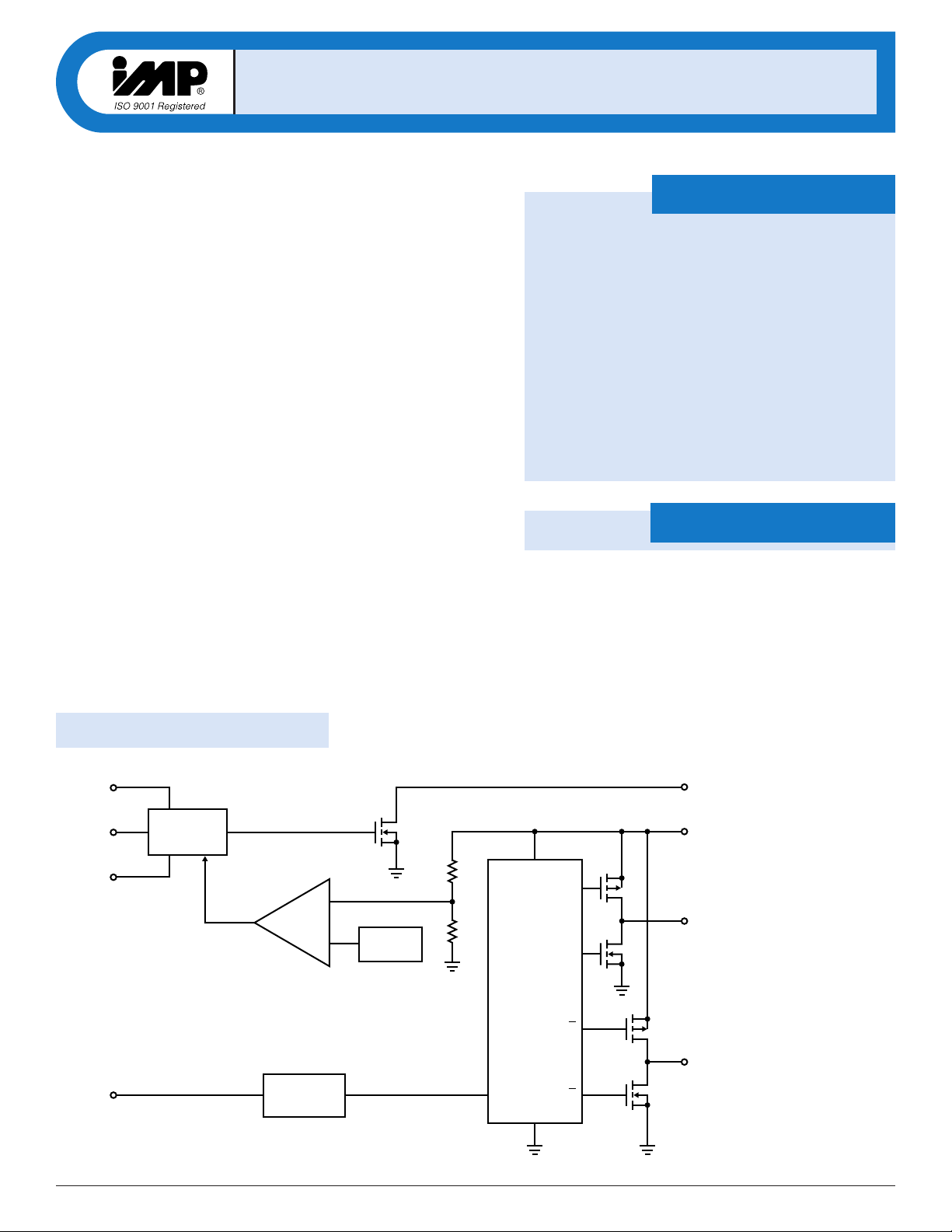
Block Diagram
–
+
527_01.eps
V
DD
1
L
X
4
C
S
3
V
A
7
V
B
6
R
SW-OSC
2
Switch
Oscillator
Regulation
Control
IMP527
Bridge
Output
Driver
Q
Q
Q
V
REF
Lamp Drive
Oscillator
C
GND
5
R
EL-OSC
8
Q
The IMP527 is an Electroluminescent (EL) lamp driver designed for
systems that must operate down to 1 volt and below. The input supply
voltage range is 0.9V to 2.5V. Typical output lamp drive voltage is 180V.
All four EL lamp-driving functions are on-chip. These are the switchmode power supply, its high-frequency oscillator, the high-voltage
H-bridge lamp driver and its low-frequency oscillator. EL lamps of up to
6nF capacitance can be driven to high brightness.
The circuit requires few external components; one inductor, one diode,
one capacitor and two resistors. The resistors set the frequency for the
two oscillators.
A disable mode puts the chip into a low current-drain state. When disabled, quiescent current drops to 1µA typical with a V
DD
of 1.5V. The chip
can be disabled by connecting R
SW
, the oscillator frequency setting resistor, to ground. A disable pad (active low), accessible only on the die, can
also be used to disable the driver.
An internal circuit shuts down the switching regulator when the lamp
drive voltage exceeds 180V peak-to-peak. This conserves power and
extends battery life.
The IMP527 is available in MicroSO and SO-8 packages and in die form.
Page 2
IMP52
IMP5277
2 408-432-9100/www.impweb.com © 2000 IMP, Inc.
Parameter Symbol Conditions Min Typ Max Units
ON-resistance of MOS Switch R
DS(ON)
I = 50mA 15 Ω
Operating Voltage 0.9 2.5 V
Output Voltage at C
S
V
CS
VDD= 1.5V, See Figure 1, Table 1 80 90 V
Output Voltage at C
S
V
CS
VDD= 0.9V, See Figure 1, Table 2 50 V
Output Voltage Peak-to-Peak VA-V
B
V
DD
= 1.5V, See Figure 1 180 V
P-P
Quiescent VDDSupply Current, Disabled I
QDIS
Disable = HIGH 70 nA
(Disable pin available on die only)
Quiescent V
DD
Supply Current, Disabled I
QDIS
R
SW-OSC
= GND 1.0 2.0 µA
VDD= 1.5V
Input Current at VDDPin I
DD
VDD= 0.9V to 1.5V 1.5 mA
Input Current: IDDPlus Inductor Current I
IN
VDD= 1.5V, See Figure 1, Table 1 26 32 mA
V
A-B
Output Drive Frequency f
EL
VDD= 1.5V, See Figure 1, Table 1 500 Hz
Boost Converter Switching Frequency f
SW
VDD= 1.5V, See Figure 1, Table 1 26 kHz
Switching Duty Cycle D
SW
VDD= 1.5V, See Figure 1 87.5 %
Disable Input LOW Voltage V
DISL
GND 0.2 V
(Disable pin available on die only)
Disable Input HIGH Voltage V
DISH
VDD-0.5V V
DD
V
(Disable pin available on die only)
Ordering Information
Pin Configuration
4L
X
3C
S
2R
SW-OSC
1V
DD
5 GND
6V
B
7V
A
8R
EL-OSC
527_02.eps
IMP527
SO/MicroSO
Part Number Input Voltage Regulated Output Voltage Temperature Range Pins-Package
IMP527EMA 0.9V to 2.5V YES – 40°C to +85°C 8-MicroSO
IMP527ESA 0.9V to 2.5V YES – 40°C to +85°C 8-SO
IMP527/D* 0.9V to 2.5V YES 25°C Dice
IMP527/D1** 0.9V to 2.5V YES 25°C Dice
Absolute Maximum Ratings
Supply Voltage, VDD, V
RSW-OSC
and V
REL-OSC
. . – 0.5V to +3.5V
Storage Temperature Range . . . . . . . . . . . . . . . . – 65°C to +150°C
Power Dissipation (SO package) . . . . . . . . . . . . 400mW
Power Dissipation (MicroSO package) . . . . . . . 300mW
Unless otherwise noted, V
DD
= 1.5V, RSW= 1MΩ, REL= 1MΩ, and TA= 25°C.
Note: All voltages are referenced to GND.
These are stress ratings only and functional operation is not implied.
Exposure to absolute maximum ratings for prolonged time periods may
affect device reliability.
Electrical Characteristics
* Disable pad not active
** Disable pad active
Page 3
IMP52
IMP5277
© 2000 IMP, Inc.
Electroluminescent Lamp Driver
3
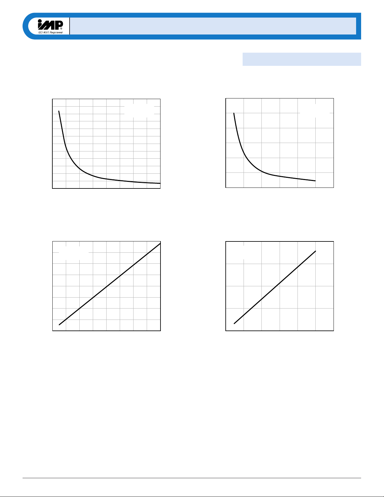
Typical Characteristics
Frequency (Hz)
REL (MΩ)
EL Lamp Drive Frequency
527_08.eps
VDD= 1.5V
TA= 25°C
0 0.5 1.0 1.5 2.0 2.5 3.0 3.5 4.0
0
400
800
1200
1600
2000
2400
Frequency (kHz)
RSW (MΩ)
527_10.eps
0 0.5 1.0 1.5 2.0 2.5 3.0
0
25
50
75
100
125
150
Boost Converter
Switching Frequency
VDD= 1.5V
TA= 25°C
Period (ms)
REL (MΩ)
527_07.eps
0 0.5 1.0 1.5 2.0 2.5 3.0 3.5 4.0
0
1
2
3
4
5
6
7
8
EL Lamp Drive Period
VDD= 1.5V
TA= 25°C
Period (ms)
RSW (MΩ)
527_09.eps
0 0.5 1.0 1.5 2.0 2.5 3.0
0
25
50
75
100
Boost Converter
Switching Period
VDD= 1.5V
TA= 25°C
Page 4

IMP52
IMP5277
4 408-432-9100/www.impweb.com © 2000 IMP, Inc.
Pin Descriptions
Pin Number Name Function
1V
DD
Positive voltage supply for the IMP527. Inductor L may be connected here or to a
separate supply.
2R
SW-OSC
Switch-mode resistor pin. Switching frequency is determined by external resistor RSW,
connected between pin 2 and VDD.
3C
S
Boost converter storage capacitor. The voltage across the EL lamp is equal to twice the
voltage at CS.
4L
X
Connection to flyback inductance, L.
5 GND Ground pin.
6V
B
EL lamp drive. The lamp is connected to a high-voltage bridge circuit with VBproviding
the complementary connection to VA.
7V
A
EL lamp drive. (See above)
8R
EL-OSC
The EL lamp oscillator frequency-setting pin. The frequency is controlled by resistor REL,
connected from pin 8 to VDD.
Disable Pad DIS Available only in die form. Setting DIS HIGH disables the chip.
External Component Description and Selection Guide
Diode A fast reverse recovery diode, with BV > 100, such as a 1N4148.
Capacitor C
S
The high voltage capacitor that stores the inductive energy transferred through the
catch diode. A 100 volt capacitor between 10nF and 100nF is recommended.
Resistor R
EL
The EL lamp oscillator frequency-setting resistor. RELis connected between pin 8 and VDD,
providing a frequency inversely proportional to REL; as RELincreases, the EL lamp frequency
decreases along with the current drawn by the lamp. Lamp color is also determined by this
frequency. A 1MΩ resistor between the R
EL-OSC
pin and the VDDsupply results in a lamp
frequency around 500Hz.
Resistor R
SW
Switching Oscillator frequency-setting resistor. RSWis connected between the R
SW-OSC
pin and
the VDDsupply. The switching frequency is inversely proportional to the resistor value, dropping
as the resistance increases.
Capacitor C
SW
This is an optional noise-suppression capacitor connected from ground to the R
SW-OSC
pin.
A 100pF capacitor is recommended.
Inductor L The inductor provides the voltage boost needed by means of inductive “flyback”. The internal
MOSFET switch alternately opens and closes the ground connection for the inductor at the
LXpin. When the switch opens, the inductor potential will forward-bias the diode
and the current will pass through to the storage capacitor CS, charging it to a high voltage.
As the value of the inductor is increased, the switching frequency set by R
SW
should also be
increased to prevent saturation. In general, smaller value inductors that can handle more current
are more desirable when larger-area EL lamps must be driven.
A small electrolytic capacitor (10µF, 16V), normally present across the inductor supply VIN,
will likely eliminate the need for CSW.
External Components
Page 5

IMP52
IMP5277
© 2000 IMP, Inc.
Electroluminescent Lamp Driver
5
+
–
V
DD
R
SW-OSC
C
S
L
X
R
EL-OSC
V
A
V
B
GND
8
7
6
5
1
2
3
4
IMP527
R
EL
R
SW
C
S
V
DD
0.1µF
1
1N4148
D
L
3nF
Note:
1. Larger values may be required depending upon supply impedance.
* Optional
527_03.eps
0.1µF
100V
CSW*
0.1nF
ON = V
DD
OFF = 0V
Figure 1. Test Circuit
Test Circuit
Figure 1 shows the IMP527 configured to drive an EL lamp,
represented as a 3nF capacitor.
Component Connections Value Description
R
SW
VDD, R
SW-OSC
1MΩ Boost converter oscillator bias resistor
R
EL
VDD, R
EL-OSC
1MΩ EL lamp driver oscillator bias resistor
LV
DD
, L
X
2
330µH
2
Boost converter inductor
C
S
CS, GND 0.1µF/100V Boost converter storage capacitor
DL
X
, C
S
1N4148 Switching diode
C
SW
R
SW-OSC
, GND 0.1nF Noise-suppression capacitor (optional)
Table 1. VIN= 1.5V
Notes. 2. Murata LQH4N331K04 (8.2Ωmax. DCR)
Component Connections Value Description
R
SW
VDD, R
SW-OSC
1MΩ Boost converter oscillator bias resistor
R
EL
VDD, R
EL-OSC
2.62MΩ EL lamp driver oscillator bias resistor
LV
DD
, L
X
3
680µH
3
Boost converter inductor
C
S
CS, GND 0.1µF/100V Boost converter storage capacitor
DL
X
, C
S
1N4148 Switching diode
C
SW
R
SW-OSC
, GND 0.1nF Noise-suppression capacitor (optional)
Table 2. VIN= 0.9V
Notes. 3. Coilcraft DS1608C-684 (2.2Ωmax. DCR)
Application Information
Page 6

IMP52
IMP5277
6 408-432-9100/www.impweb.com © 2000 IMP, Inc.
Enable/Disable Operation
Figure 2 shows how the IMP527 can be enabled via a logic gate that
connects R
SW
to VDD, and disabled by connecting it to ground.
RSWConnection IMP527 State
V
DD
Enabled
Ground Disabled
Figure 2. Enable/Disable Operation
Enable/Disable Table
Disable PAD Connection
(Available only with dice) IMP527 State
HIGH (VDD) Disabled
LOW (Ground) Enabled
The IMP527 can also be disabled using a pad on the die. The
Disable function pin is not available in packaged parts.
+
–
V
DD
R
SW-OSC
C
S
L
X
R
EL-OSC
V
A
V
B
GND
8
7
6
5
1
2
3
4
IMP527
R
EL
CMOS
Gate
R
SW
L
1
V
DD
0.1µF
2
1N4148
EL lamp
Note:
1. Murata part # LQH4N331K04 (DC resistance < 8.2 Ω)
2. Larger values may be required depending upon supply impedance.
* Optional
527_04.eps
ON = V
DD
OFF = 0V
0.1µF
100V
C
SW
*
0.1nF
C
S
D
High Voltages Present
The IMP527 generates high voltages and caution should
be exercised.
Manufacturer Series USA Phone Number
Toko D52FU (847) 297-0070
Coilcraft DS1608, DO1608, DT1608 (847) 639-6400
River Electronics FLC32 (310) 320-7488
Murata LQH4N (800) 831-9172
Inductor Manufacturers
Page 7

IMP52
IMP5277
© 2000 IMP, Inc.
Electroluminescent Lamp Driver
7
Inches Millimeters
Min Max Min Max
MicroSO (8-Pin)
A ––––– 0.0433 –––– 1.10
A1 0.0020 0.0059 0.050 0.15
A2 0.0295 0.0374 0.75 0.95
b 0.0098 0.0157 0.25 0.40
C 0.0051 0.0091 0.13 0.23
D 0.1142 0.1220 2.90 3.10
e 0.0256 BSC 0.65 BSC
E 0.193 BSC 4.90 BSC
E1 0.1142 0.1220 2.90 3.10
L 0.0157 0.0276 0.40 0.70
a0° 6° 0° 6°
SO (8-Pin)
A 0.053 0.069 1.35 1.75
A1 0.004 0.010 0.10 0.25
B 0.013 0.020 0.33 0.51
C 0.007 0.010 0.19 0.25
e 0.050 1.27
E 0.150 0.157 3.80 4.00
H 0.228 0.244 5.80 6.20
L 0.016 0.050 0.40 1.27
D 0.189 0.197 4.80 5.00
SO (8-Pin)
Package Dimensions
MicroSO (8-Pin)
a
E1 E
+
L
D
A2
A
0.10mm
D
e
b
0.004in
A1
C
MicroSO (8-Pin).eps
0°– 8°
N
L
H
E
D
A
e
B
A1
C
SO (8-Pin).eps
Page 8

IMP, Inc.
Corporate Headquarters
2830 N. First Street
San Jose, CA 95134-2071
Tel: 408-432-9100
Fax: 408-434-0335
e-mail: info@impinc.com
http://www.impweb.com
The IMP logo is a registered trademark of IMP, Inc.
All other company and product names are trademarks of their respective owners.
©
2000 IMP, Inc.
Printed in USA
Publication #: 2003
Revision: B
Issue Date: 07/11/00
Type: Product
IMP52
IMP5277
 Loading...