

Datasheet IMP38HC45ESD, IMP38HC45EPD, IMP38HC45EPA, IMP38HC42ESD, IMP38HC42ESA Datasheet (IMP)
...Page 1
© 2000 IMP, Inc. 408-432-9100/www.impweb.com 1
IMP38C/HC/42/3/4/5
IMP38C/HC/42/3/4/5
POWER MANAGEMENT
Key Features
◆
384x Series Pinout with BiCMOS Technology
◆
Zero Cross-Conduction Current by Design
◆
1MHz Operation
◆
65ns Maximum Current-Sense Delay
◆
120µA Maximum Start-Up Current
◆
1.5mA Maximum Operating Current
◆
High Output Current Drive
– 1.0A, IMP38HC4x
– 0.5A, IMP38C4x
◆
20V Maximum Supply Voltage
◆
2.5V, 1%, Trimmed Error Amplifier Reference
◆
Trimmed Oscillator Discharge Current
◆
Pin-for-Pin Enhanced Replacements for Micrel
MIC38C/HC4x and GMT38C4x/HC4x
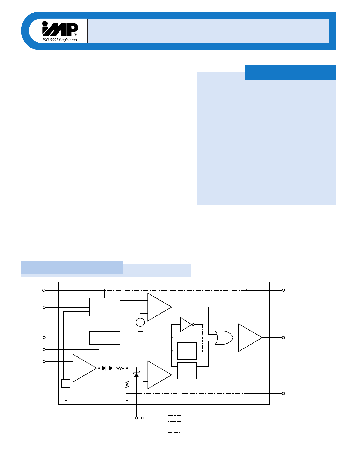
Block Diagrams
BiCMOS Cur
BiCMOS Currr
ent-Mode
ent-Mode
PWM Contr
PWM Contr
oller
ollerss
– – 1MHz Oper
1MHz Oper
ation
ation
– – NNo Cr
o Crososss--
Conduction Cur
Conduction Currr
ent
ent
– – 50ns Cur
50ns Currr
ent-Sense Dela
ent-Sense Delayy
The IMP38C4x and IMP38HC4x are fixed frequency, high performance,
current-mode PWM controllers that are pin compatible with bipolar 384x
devices but feature improvements resulting from IMP’s BiCMOS
processing and circuit design. Notable among the improvements are zero
cross-conduction/shoot-through current, reduced start-up and operating
current, lower current-sense delay, higher frequency operation, full
supply voltage swing at the output and a 1% trimmed voltage reference.
IMP38C4x and IMP38HC4x output driver stage has zero cross-conduction
current. A proprietary output state-machine monitors each output
MOSFET and guarantees by design zero cross-conduction current. This is
an industry first for 384x PWM devices.
Under-voltage lockout (UVL) performance has been improved. When
the power supply voltage is below the startup voltage, internal circuitry
puts the output into a low impedance state. The output will sink 20mA
and remain below 1.3V, well below the turn-on threshold voltage of the
external MOSFET. Even when V
DD
drops to zero volts, the out pin will
not rise above approximately 1.3V because the output UVLO circuit is
+
–
EA
OUT
6 (10)
RTCT
4 (7)
COMP
1 (1)
V
DD
V
REF
5V
Reference
7 (12)
8 (14)
FB
2 (3)
V
D
(11)
–
+
+
–
UVLO
+
–
COMP
PGND
(8)
Oscillator
TQ
S
Q
R
1V
R
2R
2.5V
Ref
( ) Pins Are 14-Pin Devices Only
38C/HC_01.eps
+
–
GND 5
AGND (9)
3 (5)
ISNS
Connection Notes
IMP38C4X, IMP38HC4X (8-Pin Devices)
50% Maximum Duty Cycle:
IMP38C44, IMP38HC44, IMP38C45, IMP38HC45
96% Maximum Duty Cycle:
IMP38C42, IMP38HC42, IMP38C43, IMP38HC43
Page 2

IMP38C/HC/42/3/4/5
IMP38C/HC/42/3/4/5
2 408-432-9100/www.impweb.com © 2000 IMP, Inc.
!S
Pin Descriptions
Pin Configuration
IMP38C4x
IMP38HC4x
1COMP
2FB
3ISNS
4RT/CT
V
REF
V
DD
OUT
GND
8
7
6
5
38C/HC_02.eps
SO/MicroSO/DIP SO/DIP
IMP38C4x
IMP38HC4x
1COMP
2NC
3FB
4NC
V
REF
NC
V
DD
V
D
14
13
12
11
5ISNS OUT10
6NC AGND9
7RT/CT PGND8
38C/HC_03.eps
powered through the out pin. Leakage current from the external
power MOSFETs will not force the PWM output to rise and turn
the external MOSFETs on.
Current-sense propagation delay time is 35ns typical, 65ns maximum, representing an up to 75 percent reduction over other 38xx
implementations.
Output stage drive is 0.5A for IMP38C4x devices. The high-drive
IMP38HC4x family is rated at 1.0A peak current drive.
Like conventional 384x controllers, the IMP38C4x and
IMP38HC4x controllers use the current-mode architecture for
superior load regulation, pulse-by-pulse current limiting and output MOSFET protection. All versions operate up to 20 volts.
For maximum application flexibility, start-up voltage ranges from
14.5V to 8.4V. Start-up current has been reduced to 120µA maxi-
mum and operating current has been reduced to 1.5mA maximum.
The IMP38C4x/IMP38HC4x are available in 8-pin and 14-pin DIP
and SO packages as well as the 8-pin MicroSO package. The 14pin devices provide separate pins for the controller power supply
and the output driver supply. This configuration maximizes
application flexibility and performance. The 14-pin package can
also dissipate more power. Devices in the compact 8-pin packages
do not have separate output drive supply connections.
The IMP38C4x and IMP38HC4x families operate over the –40°C
to +85°C temperature range.
rebmuNniP
egakcaPniP-8egakcaPniP-41
11 PMOC .rotarapmocMWPehtottupnidnareifilpmarorrEehtfotuptuO
23BF.reifilpmArorrEehtfotupnignitrevnI
35SNSI.V1otdetimilyllanretnisitI.tupnirotarapmocesnestnerruC
47 TC/TR
58 DNGP/DNG
601TUO
721V
841V
9DNGA.egakcapnip-41rofnoitcennocdnuorggolanA
11V
31,6,4,2CN.noitcennoclanretnioN
emaNnoitcnuF
V
FER
.egakcapnip-41rofdnuorg
V
CC
DD
FER
D
.tupniegatlovylppuS
.tuptuoegatlovecnerefer-V5
otdetcennocsiTRrotsiseR.noitcennoctnenopmocgnimitCRrotallicsO
dnaTRfoseulavtnereffiD.dnuorgotdetcennocsiTCroticapacdna
.elcycytudmumixamehtenimretedTC
rewopdnaseciveddegakcapnip-8rofdnuorggolanadnarewopdenibmoC
nehwWOLdlehylevitcasinipTUO.tuptuorevirdelop-metot,rewop-hgiH
.dlohserhtOLVUehtwolebsi
.egakcapnip-41rofegatlovylppusrevirdtuptuO
spe.10t_CH-C83
Page 3
IMP38C/HC/42/3/4/5
IMP38C/HC/42/3/4/5
© 2000 IMP, Inc.
PWM Controllers
3
Ordering Information
For SO and MicroSO packages, append “/T” to the ordering part number for tape and reel packaging.
gniredrOPMI
rebmuNtraPegakcaP
APE24C83PMIPIDcitsalP-8 – 04 ° 58otC °CV5.41V0.9%69V5.2A5.0
DPE24C83PMIPIDcitsalP-41 – 04 ° 58otC °CV5.41V0.9%69V5.2A5.0
ASE24C83PMIOS-8 – 04 ° 58otC °CV5.41V0.9%69V5.2A5.0
DSE24C83PMIOS-41 – 04 ° 58otC °CV5.41V0.9%69V5.2A5.0
AME24C83PMIOSorciM-8 – 04 ° 58otC °CV5.41V0.9%69V5.2A5.0
D/24C83PMIEID
APE34C83PMIPIDcitsalP-8 – 04 ° 58otC °CV4.8V6.7%69V5.2A5.0
DPE34C83PMIPIDcitsalP-41 – 04 ° 58otC °CV4.8V6.7%69V5.2A5.0
ASE34C83PMIOS-8 – 04 ° 58otC °CV4.8V6.7%69V5.2A5.0
DSE34C83PMIOS-41 – 04 ° 58otC °CV4.8V6.7%69V5.2A5.0
AME34C83PMIOSorciM-8 – 04 ° 58otC °CV4.8V6.7%69V5.2A5.0
D/34C83PMIEID
APE44C83PMIPIDcitsalP-8 – 04 ° 58otC °CV5.41V0.9%05V5.2A5.0
DPE44C83PMIPIDcitsalP-41 – 04 ° 58otC °CV5.41V0.9%05V5.2A5.0
ASE44C83PMIOS-8 – 04 ° 58otC °CV5.41V0.9%05V5.2A5.0
DSE44C83PMIOS-41 – 04 ° 58otC °CV5.41V0.9%05V5.2A5.0
AME44C83PMIOSorciM-8 – 04 ° 58otC °CV5.41V0.9%05V5.2A5.0
D/44C83PMIEID
APE54C83PMIPIDcitsalP-8 – 04 ° 58otC °CV4.8V6.7%05V5.2A5.0
DPE54C83PMIPIDcitsalP-41 – 04 ° 58otC °CV4.8V6.7%05V5.2A5.0
ASE54C83PMIOS-8 – 04 ° 58otC °CV4.8V6.7%05V5.2A5.0
DSE54C83PMIOS-41 – 04 ° 58otC °CV4.8V6.7%05V5.2A5.0
AME54C83PMIOSorciM-8 – 04 ° 58otC °CV4.8V6.7%05V5.2A5.0
D/54C83PMIEID
APE24CH83PMIPIDcitsalP-8 – 04 ° 58otC °CV5.41V0.9%69V5.2A0.1
DPE24CH83PMIPIDcitsalP-41 – 04 ° 58otC °CV5.41V0.9%69V5.2A0.1
ASE24CH83PMIOS-8 – 04 ° 58otC °CV5.41V0.9%69V5.2A0.1
DSE24CH83PMIOS-41 – 04 ° 58otC °CV5.41V0.9%69V5.2A0.1
AME24CH83PMIOSorciM-8 – 04 ° 58otC °CV5.41V0.9%69V5.2A0.1
D/24CH83PMIEID
APE34CH83PMIPIDcitsalP-8 – 04 ° 58otC °CV4.8V6.7%69V5.2A0.1
DPE34CH83PMIPIDcitsalP-41 – 04 ° 58otC °CV4.8V6.7%69V5.2A0.1
ASE34CH83PMIOS-8 – 04 ° 58otC °CV4.8V6.7%69V5.2A0.1
DSE34CH83PMIOS-41 – 04 ° 58otC °CV4.8V6.7%69V5.2A0.1
AME34CH83PMIOSorciM-8 – 04 ° 58otC °CV4.8V6.7%69V5.2A0.1
D/34CH83PMIEID
APE44CH83PMIPIDcitsalP-8 – 04 ° 58otC °CV5.41V0.9%05V5.2A0.1
DPE44CH83PMIPIDcitsalP-41 – 04 ° 58otC °CV5.41V0.9%05V5.2A0.1
ASE44CH83PMIOS-8 – 04 ° 58otC °CV5.41V0.9%05V5.2A0.1
DSE44CH83PMIOS-41 – 04 ° 58otC °CV5.41V0.9%05V5.2A0.1
AME44CH83PMIOSorciM-8 – 04 ° 58otC °CV5.41V0.9%05V5.2A0.1
D/44CH83PMIEID
APE54CH83PMIPIDcitsalP-8 – 04 ° 58otC °CV4.8V6.7%05V5.2A0.1
DPE54CH83PMIPIDcitsalP-41 – 04 ° 58otC °CV4.8V6.7%05V5.2A0.1
ASE54CH83PMIOS-8 – 04 ° 58otC °CV4.8V6.7%05V5.2A0.1
DSE54CH83PMIOS-41 – 04 ° 58otC °CV4.8V6.7%05V5.2A0.1
AME54CH83PMIOSorciM-8 – 04 ° 58otC °CV4.8V6.7%05V5.2A0.1
D/54CH83PMIEID
erutarepmeT
egnaR
putratS
egatloV
gnitarepO
muminiM
gnitarepO
egatloV
mumixaM
elcyCytuD
ecnerefeR
egatloV
tuptuOkaeP
evirDtnerruC
spe.20t_CH/C83
Page 4

IMP38C/HC/42/3/4/5
IMP38C/HC/42/3/4/5
4 408-432-9100/www.impweb.com © 2000 IMP, Inc.
!S
Absolute Maximum Ratings
VCCSupply Voltage . . . . . . . . . . . . . . . . . . . . . . 20V
V
CC
Supply Current . . . . . . . . . . . . . . . . . . . . . . 30mA
I
OUT
Current . . . . . . . . . . . . . . . . . . . . . . . . . . . . 1.0A
Current-Sense and Feedback Inputs . . . . . . . . 0.3V to 5.5V
Operation Junction Temperature . . . . . . . . . . . +150°C
Storage Temperature . . . . . . . . . . . . . . . . . . . . . – 65°C to +150°C
Lead Soldering Temperature (10 seconds) . . . +300°C
Parameter Symbol Conditions Min Typ Max Units
Reference
Output voltage V
REF
TA= +25°C, IO= 1mA 4.90 5.00 5.10 V
Line Regulation 12V ≤ V
CC
≤ 18V, I
OUT
= 5µA220mV
Load Regulation 1mA ≤ IO≤ 20mA 1 25 mV
Temperature Stability TC
REF
Note 1 0.2 mV/°C
Total Reference Variation Line, Load, Temperature, Note 1 4.82 5.18 V
Output Noise Voltage V
N
10Hz ≤ f ≤ 10kHz, TA= +25°C, Note 1 50 µV
Long Term Stability TA= 125°C, 1000 Hours, Note 1 TBD mV
Output Short Circuit I
SC
–30 –40 –180 mA
Oscillator Section
Initial Accuracy f
INIT
TA= 25°C, Note 5 49 52 55 kHz
Voltage Stability 12V ≤ VCC≤ 18V 0.2 1.0 %
Temperature Stability TC
OSC
Note 1 0.04 %/°C
Discharge Current V
RT/CT
= 2V 7.2 8.4 12.0 mA
Amplitude peak-to-peak V
OSC, P-P
V
RT/CT
peak-to-peak 1.1 1.7 2.3 V
Error Amplifier Section
Input Voltage V
IN
V
COMP
= 2.5V 2.45 2.50 2.55 V
Input Bias Current I
B
VFB= 4.5V –11µA
Open Loop Gain A
VOL
2V ≤ VO≤ 4V, Note 1 65 90 dB
Unity Gain Bandwidth UGBW Note1 0.7 1.0 MHz
Power Supply Rejection Ratio PSRR V
START
≤ VCC≤ V
CCMAX
60 dB
Output Sink Current I
OL
VFB= 2.7V, Vcomp = 1.1V 2 6 mA
Output Source Current I
OH
VFB= 2.3V, Vcomp = 5.0V –0.5 –1.0 mA
V
OUT
High V
OH
VFB= 2.3V, RL= 15kΩ to ground 4.5 4.6 5.0 V
V
OUT
Low V
OL
VFB= 2.7V, RL= 15kΩ to V
REF
0.30 0.50 V
Unless otherwise noted, VCC= 15V, RT = 10kΩ and CT = 3.3nF. Specifications are over the – 40°C to +85°C ambient temperature range.
Bold/blue specifications indicate enhanced performance features.
Electrical Characteristics
Package Thermal Resistance
8-Pin Plastic DIP (θ
JA
) . . . . . . . . . . . . . . . . . 125°C/W
8-Pin MicroSO (θ
JA
) . . . . . . . . . . . . . . . . . . . 250°C/W
8-Pin SO (θ
JA
) . . . . . . . . . . . . . . . . . . . . . . . . 170°C/W
14-Pin Plastic DIP (θ
JA
) . . . . . . . . . . . . . . . . 90°C/W
14-Pin SO (θ
JA
) . . . . . . . . . . . . . . . . . . . . . . . 145°C/W
Note: All voltages are referenced to GND.
These are stress ratings only and functional operation is not
implied. Exposure to absolute maximum ratings for prolonged
time periods may affect device reliability.
Page 5

IMP38C/HC/42/3/4/5
IMP38C/HC/42/3/4/5
© 2000 IMP, Inc.
PWM Controllers
5
Electrical Characteristics
Parameter Symbol Conditions Min Typ Max Units
Current Sense
Gain A
VOL
Notes 1, 2 and 3 2.90 3.00 3.10 V/V
Over Current Protection Threshold Vcomp = max, Note 2 0.9 0.98 1.1 V
Power Supply Rejection Ratio PSRR V
START
≤ VCC≤ 18V 70 dB
Input Bias Current I
B
–0.1 – 2.0 µA
Delay to Output T
PD
VFB= 0V, ISNS 0V to 2V, CL= 1nF 50 65 ns
Output
IMP38C4x
ON Resistance, High R
DS (ON)ISOURCE
= 0.2A 20 Ω
ON Resistance, Low I
SINK
= 0.2A 11
IMP38HC4x
ON Resistance, High R
DS (ON)ISOURCE
= 0.2A 10 Ω
ON Resistance, Low I
SINK
= 0.2A 5.5
Peak Drive Current HC devices 1.0 A
H devices 0.5
IMP38C4x Rise Time T
R
TA= 25°C, CL= 1nF 40 70 ns
IMP38C4x Fall Time T
F
TA= 25°C, CL= 1nF 30 50 ns
IMP38HC4x Rise Time T
R
TA= 25°C, CL= 1nF 20 50 ns
IMP38HC4x Fall Time T
F
TA= 25°C, CL= 1nF 15 40 ns
Shoot-through Current 0mA
Undervoltage Lockout
Start Threshold IMP38C42/4, IMP38HC42/4 13.5 14.5 15.5 V
IMP38C43/5, IMP38HC43/5 7.8 8.4 9.0
Minimum Operating Voltage IMP38C42/4, IMP38HC42/4 8 9 10 V
IMP38C43/5, IMP38HC43/5 7.0 7.6 8.2
Pulse Width Modulator
Maximum Duty Cycle IMP38C42/3, IMP38HC42/3, 94 96 %
Maximum Duty Cycle IMP38C44/5, IMP38HC44/5 48 50 %
Minimum Duty Cycle 0%
Supply Current
Start-Up Current VCC= 13V for IMP38C42/44, IMP38HC42/44 95 120 µA
VCC= 7.5V for IMP38C43/45, IMP38HC43/45
Operating Current I
CC
VFB= VIS= 0 0.5 1.5 mA
Unless otherwise noted, VCC= 15V, RT= 10kΩ and CT= 3.3nF. Specifications are over the – 40°C to +85°C ambient temperature range.
Bold/blue specifications indicate enhanced performance features.
Note 1. Guaranteed by design. Not 100% tested in production.
Note 2. Measured at trip point of V
FB
= 0V.
Note 3. Gain is defined as:
Table 1. Startup and Operating Voltage Selection Guide
A
V
V
, 0 V 0.8V
COMP
CS
CS
=≤≤
∆
∆
Note 4. Adjust VCCabove the start threshold before setting at 15V.
Note 5. Output frequency equals the oscillator frequency for
IMP38C42/3 and IMP38HC42/3 devices. Output frequency
equals one-half the oscillator frequency for IMP38C44/5 and
IMP38HC44/5 devices.
sdlohserhTOLVU
V4.8tapu-tratS
elcyCytuD
%69ot%034CH/34C83PMI24CH/24C83PMI
%05ot%054CH/54C83PMI44CH/44C83PMI
V6.7=muminiMgnitarepO
V5.41tapu-tratS
V0.9=muminiMgnitarepO
spe.30t_CH/C83
Page 6

IMP38C/HC/42/3/4/5
IMP38C/HC/42/3/4/5
6 408-432-9100/www.impweb.com © 2000 IMP, Inc.
!S
Transient Protection
Good high-frequency layout practices should be followed. Avoid
long printed-circuit traces and component leads. Locate oscillator
and compensation components near the IC. Avoid capacitive and
inductive coupling of the switching waveform into the
high-impedance inputs of the error amplifier, oscillator, and
current-sense amplifier. V
REF
and VCCstability will be aided by
using high-frequency decoupling capacitors.
Undervoltage Lockout
Several different thresholds are available.
Under-voltage lockout (UVL) performance has been improved.
When the power supply voltage is below the startup voltage,
internal circuitry puts the output into a low impedance state and
sets the output to zero. The output will sink up to 20mA in this
controlled state and remain below 1.3V, well below the turn-on
threshold voltage of the external MOSFET.
With the IMP38C/HC4x output stage design, leakage current
from the external power MOSFETs will not force the PWM output
to rise and turn the external MOSFET on.
Even when V
DD
drops to zero volts, the OUT pin will not rise
above approximately 1.3V because the UVLO circuit is powered
through the OUT pin.
The IMP output stage performance in UVL mode, while sinking
20mA, is shown in Figure 2.
Figure 2. Output Stage Performance in UVL Mode
0
Output
(V)
VDD (V)
2.0
1.5
1.0
0.5
0
V
OUT
While Sinking 20mA
12345 7698
38C/HC_05b.eps
IMP38C/HC4x
sdlohserhTtuokcoLegatlovrednU
V4.8tapu-tratS
V6.7=muminiMgnitarepO
V5.41tapu-tratS
V0.9=muminiMgnitarepO
34CH/34C83PMI24CH/24C83PMI
54CH/54C83PMI44CH/44C83PMI
spe.40t_CH/C83
The IMP38C and IMP38HC devices are compatible with generic
384x PWM devices. The following discussion highlights the differences and advantages of the IMP ‘C’ and ‘HC’ designs.
Start-up Current
IMP’s BiCMOS process allows for substantial reduction in the
start-up current. Typical start-up current is 95µA, with a maximum limit of 120µA. Low start-up current allows high resistance,
lower-wattage, start-up resistors to supply controller start-up
power.
Operating Current
Operating current has been reduced to 1.5mA maximum.
Compared to the 11mA needed for a typical bipolar controller and
6mA for competitive BiCMOS controllers, IMP's low operating
current allows the controller to run cooler and with better efficiency. In addition, the V
CC
hold-up capacitance (used during
start-up) can be reduced.
Output Driver
The IMP38HC4x/38C4x CMOS output stage drives external
power MOSFETs to the full supply voltage. Low ON-resistance
and high peak current drive combine to give greater than 1000pF
gate capacitance drive capability. Rise and fall time requirements
may dictate the appropriate value of output capacitance. Within
the restrictions of output capacity and controller power dissipation, switching frequencies can exceed 1MHz.
The CMOS output stage “break-before-make” action is guaranteed by design and insures that no cross-conduction current will
flow. This minimizes heat dissipation, increases efficiency and
enhances reliability.
Oscillator Operation
Two external components, RT and CT, set the switching frequency.
With V
CC
= 14V, RT = 10k and CT = 3.3nF, nominal switching
frequency is 50kHz.
Figure 1. Oscillator Component Selection
Application Information
frequency Hz
1.73
RT CT F
[]
=
[]×[]
Ω
IMP38C4x
IMP38HC4x
V
REF
RT/CT
GND
38C/HC_07.eps
RT
CT
Page 7

IMP38C/HC/42/3/4/5
IMP38C/HC/42/3/4/5
© 2000 IMP, Inc.
PWM Controllers
7
Application Information
OUT
6 (10)
V
D
(11)
–
+
+
–
UVLO
+
–
COMP
PGND
(8)
TQ
S
Q
R
UVL
Protection
1V
R
2R
( ) Pins Are 14-Pin Devices Only
38C/HC_06.eps
GND 5
AGND (9)
3 (5)
ISNS
Connection Notes
IMP38C4X, IMP38HC4X (8-Pin Devices)
50% Maximum Duty Cycle:
IMP38C44, IMP38HC44, IMP38C45, IMP38HC45
96% Maximum Duty Cycle:
IMP38C42, IMP38HC42, IMP38C43, IMP38HC43
Figure 3. UVL Protection Circuit
Page 8

IMP38C/HC/42/3/4/5
IMP38C/HC/42/3/4/5
8 408-432-9100/www.impweb.com © 2000 IMP, Inc.
!S
Plastic DIP (8-Pin)
L
0°– 8°
C
H
E
e
D
B
A1
A
SO (8-Pin).eps
SO (8-Pin)
e
b
D
E1 E
a
L
+
C
D
0.10mm
0.004in
A1
A2
A
MicroSO (8-Pin).eps
sehcnIsretemilliM
niMxaMniMxaM
*)niP-8(OSorciM
A ––––– 3340.0 –––– 01.1
1A0200.09500.0050.051.0
2A5920.04730.057.059.0
b8900.07510.052.004.0
C1500.01900.031.032.0
D2411.00221.009.201.3
eCSB6520.0CSB56.0
ECSB391.0CSB09.4
1E2411.00221.009.201.3
L7510.06720.004.007.0
a °0 °6 °0 °6
**)niP-8(OS
A350.0960.053.157.1
1A400.0010.001.052.0
B310.0020.033.015.0
C700.0010.091.052.0
e050.072.1
E051.0751.008.300.4
H822.0442.008.502.6
L610.0050.004.072.1
D981.0791.008.400.2
***)niP-8(PIDcitsalP
A ––––– 012.0 –––– 33.5
1A510.0 ––––– 83.0 –––––
2A511.0591.029.259.4
b410.0220.063.065.0
2b540.0070.041.187.1
3b030.0540.008.041.1
D553.0004.020.961.01
1D500.0 ––––– 31.0 –––––
E003.0523.026.762.8
1E042.0082.001.611.7
e001.0 ––––– 45.2
Ae003.0 ––––– 26.7
Be ––––– 034.0 ––––– 29.01
Ce ––––– 060.0
L511.0051.029.218.3
AA781-OMgniwarDCEDEJ*
AA211-SMgniwarDCEDEJ**
AB100-SMgniwarDCEDEJ***
3ta.50t_CH/C83
SO (8-Pin)
SO (8-Pin)
Package Dimensions
A2
A
L
A1
D1
D
e
b2
b
0°–15°
E
E1
C
eA
eB
Plastic DIP (8-Pin)a.eps
Page 9

IMP38C/HC/42/3/4/5
IMP38C/HC/42/3/4/5
© 2000 IMP, Inc.
PWM Controllers
9
Package Dimensions
D1
D
eA
C
0°–15°
A
E1 E
e1
B1
B
L
A1
Plastic DIP (14-Pin).eps
Plastic DIP (14-Pin)
SO (14-Pin)
H
E
eB
D
A1
A
SO (16-Pin).eps
L
0°– 8°
C
sehcnIsretemilliM
niMxaMniMxaM
*)niP-41(OS
A6290.03401.053.256.2
1A0400.0811.001.003.0
B310.0020.033.015.0
C1900.05210.032.023.0
D5643.02263.008.802.9
E412.02992.004.706.7
eCSB050.0CSB72.1
H493.0914.000.0156.01
L610.0050.004.072.1
**)niP-41(PIDcitsalP
A551.0002.049.380.5
1A02.005.015.072.1
B410.0020.0653.0805.0
1B050.0560.072.156.1
C800.0210.0402.0403.0
D547.0077.039.8155.91
E003.0523.026.752.8
1E042.0062.001.606.6
1ePYT001.0PYT45.2
AePYT003.0PYT26.7
L001.0 ––––– 81.318.3
FA310-SMgniwarDCEDEJ*
BA-AA100-OMgniwarDCEDEJ**
3ta.60t_CH/C83
Page 10

IMP, Inc.
Corporate Headquarters
2830 N. First Street
San Jose, CA 95134-2071
Tel: 408-432-9100
Fax: 408-434-0335
e-mail: info@impinc.com
http://www.impweb.com
The IMP logo is a registered trademark of IMP, Inc.
All other company and product names are trademarks of their respective owners.
©
2000 IMP, Inc.
Printed in USA
Publication #: 3001
Revision: D
Issue Date: 08/30/00
Type: Preliminary
IMP38C/HC/42/3/4/5
IMP38C/HC/42/3/4/5
 Loading...