

Page 1
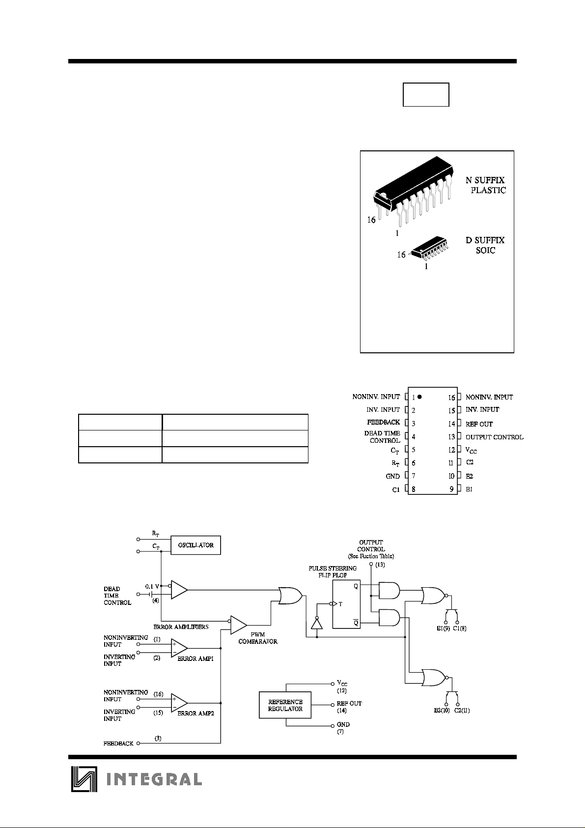
PWM Control Circuit
The IL494 incorporates on a single monolithic chip all the
functions required in the construction of a pulse-width-modulation
control circuit. Designed primarily for power supply control, the IL494
contains an on-chip 5-volt regulator, two error amplifiers, adjustable
oscillator, dead-time control comparator, pulse-steering flip-flop, and
output-control circuitry. The uncommitted output transistors provide
either common-emitter or emitter-follower output capability. Push-pull
or single-ended output operatio n may be selected through the outputcontrol function. The architecture of the IL494 prohibits the possibility
of either output being pulsed twice during push-pull operation.
•
Complete PWM Power Control Circuitry
•
Uncommitted Outputs for 200 mA Sink or Source
•
Output Control Selects Single-Ended or Push-Pull Operation
•
Internal Circuitry Prohibits Double Pulse at Either Output
•
Internal Regulator Provides a Stable 5 V Reference Supply
•
Variable Dead-Time Provides Control Over Total Range
TECHNICAL DATA
IL494
ORDERING INFORMATION
IL494N Plastic
IL494D SOIC
TA = -20°C to 85° C
for all packages
PIN ASSIGNMENT
FUNCTION TABLE
Output Control Output Function
Grounded Single-ended or Parallel Out put
At V
ref
Normal Push-Pull Operation
LOGIC DIAGRAM
1
Page 2
IL494
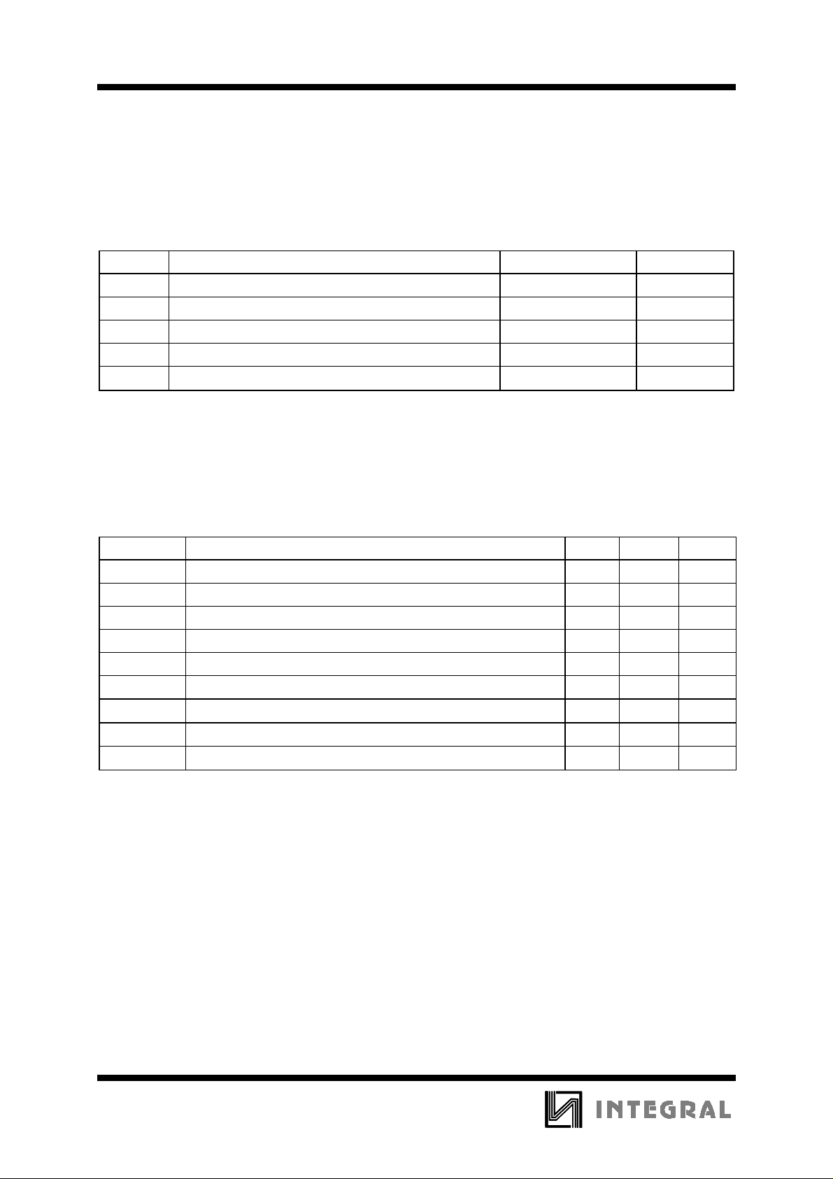
MAXIMUM RATINGS
Symbol Parameter Value Unit
V
CC
V
V
Tstg Storage Temperature -65 to +150
Supply Voltage 41 V
Amplifier Input Voltage VCC +0.3 V
I
Collector Output Voltage 41 V
O
Collector Output Current 250 mA
°
C
RECOMMENDED OPERATING CONDITIONS
Symbol Parameter Min Max Unit
V
CC
V
I
V
O
C
T
R
T
T
A
Supply Voltage 7 40 V
Amplifier Input Voltage -0.3 V
- 2 V
CC
Collector Output Voltage 40 V
Collector Output Current (Each Transistor) 200 mA
Current Into Feed back Terminal 0.3 mA
Timing Capacitor 0.47 10.000 nF
Timing Resistor 1.8 500
Oscillator Frequency 1 300 KHz
Operating Free-Air Temperature -20 +85
Ω
K
°
C
2
Page 3
IL494
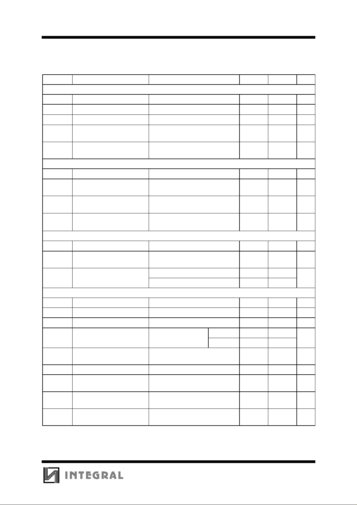
ELECTRICAL CHARACTERISTICS
(Temperature -20 ∼ 85°C, VCC = 15 V, f=10 kHz))
Symbol Parameter Test Conditions Min Max Unit
Reference Section
V
V
∆
V
regin
regout
V
ref
Output Voltage IO=1 mA 4.75 5.25 V
Output regulation
Input regulation
Output Voltage change with
ref
V
=7 V to 40 V, TA=25°C
CC
I
=1 to 10 mA, TA=25°C
O
T
= -20°C to 85°C
A
25 mV
15 mV
1%
temperature
I
SC
Short-circuit output current
Vref=0 50 mA
(Note 1)
Oscillator Section
f
δ
δ
f
OSC(∆V)
δ
f
OSC(∆T)
OSC
f
OSC
Frequency
Standard deviation of
frequency (No te 2)
Frequency change with
voltage
Frequency change with
temperature
C
=0.01 µF, RT=12 k
T
Ω
All values of VCC, CT, RT, T
Constant
VCC= 7 V to 40 V,
=25°C
T
A
C
=0.01 µF, RT=12 k
T
= -20°C to 85°C
T
A
Ω
6 14 KHz
A
15 %
10 %
2%
Dead Time Control Section
I
IB(2T)
DC
Input bias current (pin 4) VI= 0 to 5.25 V -10
Maximum duty cycle, each
max
V
=0 V 45 %
I(pin 4)
output
V
THD
Input threshold voltage Zero duty cycle 3.3 V
(pin 4) Maximum duty cycle 0
Error Amp Section
V
IO
I
IO
I
IB
Input offset voltage V
Input offset current V
Input bias current V
=2.5 V 10 mV
O(pin 3)
=2.5 V 250 nA
O(pin 3)
=2.5 V 1
O(pin 3)
Common-mode input VCC= 7 V to 40 V LOW -0.3 V
voltage range HIGH VCC - 2
A
vol
Open-loop voltage
∆
V
=3 V, VO=0.5 to 3.5 V
O
70 dB
amplification
f
b
CMRR Common-mode rejection
Unity-gain bandwidth 100 kHz
V
=40 V, TA=25°C
CC
65 dB
ratio
I
O
I
O+
Output sink current (pin 3) VID=-15 mV to -5 V,
V
=0.7 V
O(pin 3)
Output source c urrent (pin 3) VID=15 mV to 5 V,
V
=3.5 V
O(pin 3)
0.3 mA
-2 mA
µ
A
µ
A
3
Page 4
IL494
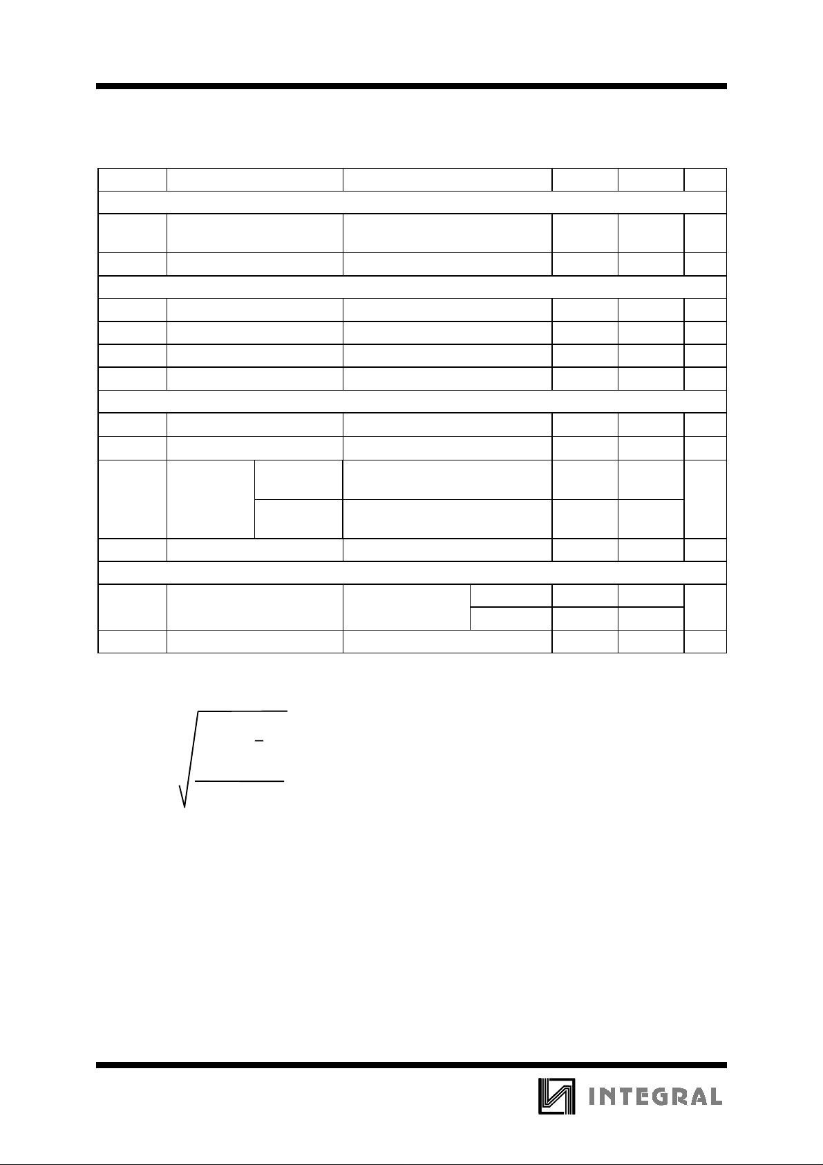
ELECTRICAL CHARACTERISTICS
(Temperature -20 ∼ 85°C, VCC = 15 V, f=10 kHz))
Symbol Parameter Test Conditions Min Max Unit
PWM Comparator Section
V
THP
Input threshold voltage
Zero duty cycle 4.5 V
(pin 3)
I
I
Input sink current (pin 3) V
=0.7 V 0.3 mA
O(pin 3)
Switching Characteristics
t
rc
t
fc
t
rf
t
ff
Output voltage rise time Common-emitter configuration 200 ns
Output voltage fall time Common-emitter configuration 100 ns
Output voltage rise time Emitter-follower configuration 200 ns
Output voltage fall time Emitter-follower configuration 100 ns
Output Section
I
C(off)
I
E(off)
V
I
SAT
OCH
Collector off-state curre nt VCE=40 V, VCC=40 V 100
Emitter off-state current VCC=VC=40 V, VE=0 -100
Collector-
emitter
saturation
voltage
Output control input current VI=V
Commonemitter
Emitterfollower
VE=0, IC=200 mA 1.3 V
VC=15 V, IE=-200 mA 2.5
ref
3.5 mA
Total Device
I
CC
Standby supply current All other inputs & VCC=15 V 10 mA
outputs open VCC=40 V 15
I
Notes:
CCA
Average supply current V
=2 V 17 mA
(pin 4)
1. Duration of the short circuit should not exceed one second.
2. Standard deviation is a measure of the statistical disribution about the mean as derived from the formula
µ
A
µ
A
N
(xn - x)
2
∑
n=1
σ
=
N - 1
4
 Loading...