

Page 1

)
)
.
.
e
600 V
700 V
800 V
IL4116
IL4117
IL4118
ZERO V OL T A GE CR OSSING
FEATURES
• High Input Sensltlvity: I
I
=3.5 mA, Typlcal PF < 1.0
FT
• Zero V oltage Crosslng
• 600/700/800 V Blocklng V oltage
• 300 mA On-State Current
• High Statlc dv/dt 10,000 V/ µ sec., typical
• Inverse Parallel SCRs Provide Commutatlng
dv/dt >10 KV/msec.
• Very Low Leakage <10 mA
• Isolation Test Voltage from Double Molded
Package 5300 VACRMS
• Package, 6-Pln DIP
• Underwriters Lab File #E52744
DESCRIPTION
The IL411x consists of an AlGaAs IRLED optically
coupled to a photosensitive zero crossing TRIAC
network. The TRIAC consists of two inverse parallel
connected monolithic SCRs. These three semiconductors are assembled in a six pin 0.3 inch dual inline package, using high insulation double molded,
over/under leadframe construction.
High input sensitivity is achieved by using an emitter follower phototransistor and a cascaded SCR
predriver resulting in an LED trigger current of less
than 1.3 mA(DC).
The IL411x uses two discrete SCRs resulting in a
commutating dV/dt greater than 10 KV/ms The use
of a proprietary dv/dt clamp results in a static dv/dt
of greater than 10 KV /µ
MOSFET that is enhanced when high dv/dt spikes
occur between MT1 and MT2 of the TRIAC. When
conducting, the FET clamps the base of the phototransistor, disabling the first stage SCR predriver.
The zero cross line voltage detection circuit consists of two enhancement MOSFETS and a photodiode. The inhibit voltage of the network is
determined by the enhancement voltage of the Nchannel FET. The P-channel FET is enabled by a
photocurrent source that permits the FET to conduct the main voltage to gate on the N-channel FET .
Once the main voltage can enable the N-channel, it
clamps the base of the phototransistor, disabling
the first stage SCR predriver.
The blocking voltage of up to 800 V permits control
of off-line voltages up to 240 VAC, with a safety factor of more than two, and is sufficient for as much as
380 VAC. Current handling capability is up to 300
mA RMS continuous at 25 °
The IL411x isolates low-voltage logic from 120, 240,
and 380 VAC lines to control resistive, inductive, or
capacitive loads including motors, solenoids, high
current thyristors or TRIAC and relays.
Applications include solid-state relays, industrial
controls, office equipment, and consumer appliances.
=1.3 mA, PF=1.0;
FT
s. This clamp circuit has a
C.
Dimensions in inches (mm)
248 (6.30)
256 (6.50)
.039
(1.00)
Min.
4°
Typ.
.018 (0.45)
.022 (0.55)
Maximum Ratings
Emitter
Reverse Voltage ...................................................................................6 V
Forward Current.............................................................................. 60 mA
Surge Current...................................................................................2.5 A
Power Dissipation.........................................................................100 mW
Derate Linearly from 25 °
Thermal Resistance................................................................... 750 °
Detector
Peak Off-State Voltage
IL4116...........................................................................................600 V
IL4117...........................................................................................700 V
IL4118...........................................................................................800 V
RMS On-State Current.................................................................. 300 mA
Single Cycle Surge.............................................................................. 3 A
Total Power Dissipation ................................................................500 mW
Derate Linearly from 25 °
Thermal Resistance.................................................................... 150 °
Package
Storage Temperature..................................................... –55 ° C to +150 ° C
Operating Temperature................................................. –55 °
Lead Soldering Temperature................................................260 °
Isolation Test Voltage...........................................................5300 VAC
Isolation Resistance
V
=500 V, T
IO
V
=500 V, T
IO
5–1
TRIAC DRIVER OPTOCOUPLER
Pin One ID.
3
4
.335 (8.50)
.343 (8.70)
12
5
6
.130 (3.30)
.150 (3.81)
.020 (.051) Min.
.031 (0.80)
.035 (0.90)
.100 (2.54) Typ.
C..................................................... 1.33 mW/ ° C
C....................................................... 6.6 mW/ ° C
=25 ° C.................................................................. ≥ 10
A
=100 ° C................................................................ ≥ 10
A
LED
Anode
LED
Cathode
NC
1
2
3
ZCC*
*Zero Crossing Circuit
.300 (7.62)
Typ.
18° Typ.
.010 (.25)
.014 (.35)
.300 (7.62)
.347 (8.82)
6
5
4
C to +100 ° C
Triac
Anode 2
Substrat
do not
connect
Triac
Anode 1
.110 (2.79
.150 (3.81
C/5 sec.
C/W
C/W
RMS
12
Ω
11
Ω
Page 2

Characteristics
(T
A
=25 ° C)
Parameter Symbol Min. Typ. Max. Unit Condition
Emitter
Forward Voltage V
Breakdown Voltage V
Reverse Current I
Capacitance C
Thermal Resistance, Junction to Lead R
F
BR
R
O
THJL
630 VI
1.3 1.5 V I
0.1 10
µ AV
40 pF V
750
°
C/W
-20 mA
F
=10 µ A
R
=6 V
R
=0 V, f=1 MHz
F
Output Detector
Repetitive Peak Off-State Voltage
IL4116
IL4117
IL4118
V
V
V
DRM
DRM
DRM
600
700
800
650
750
850
V
V
V
I
DRM
I
DRM
I
DRM
Off-State Voltage
IL4116
IL4117
IL4118
Off-State Current I
On-State Voltage V
On-State Current I
Surge (Non-Repetitive, On-State Current) I
Holding Current I
Latchiing Current I
LED Trigger Current I
Zero Cross Inhibit Voltage V
Turn-On Time t
Turn-Off Time t
Critical State of Rise: Off-State Voltage dv
Commutating Voltage dv
Commutating Current di/dt 100 A/ms I
Thermal Resistance, Junction to Lead R
V
D(RMS)
V
D(RMS)
V
D(RMS)
D(RMS)
TM
TM
TSM
H
L
FT
IH
ON
OFF
/dt 10,000
(MT)
(COM)
THJL
424
494
565
/dt 10,000
460
536
613
10 100
1.7 3 V I
V
V
V
µ AV
I
D(RMS)
I
D(RMS)
I
D(RMS)
=600 V, T
D
=300 mA
T
300 mA PF=1.0, V
3 A f=50 Hz
65 200
5mAV
0.7 1.3 mA V
15 25 V I
35
50
2000
2000
150
µ AV
µ sV
=3 V
T
=2.2 V
T
=5 V
AK
=Rated I
F
=V
RM
µ s PF=1.0, I
V/ µ s
V/ µ
V/ µ s
V/ µ s
C/W
°
V
, V
RM
s
, V
V
RM
V
, V
RM
V
, V
RM
=300 mA
T
Package
Critical State of Rise of Couplrd
Input-Output Voltage
Common Mode Coupling Capacitor C
Package Capacitance C
dv
/dt 10,000 V/ µ sI
(IO)
CM
IO
0.01 pF
0.8 pF f=1 MHz, V
=0 A, V
T
=100 mA
=100 mA
=100 mA
=70 µ A
=70 µ A
=70 µ A
T(RMS)
FT
=424 VAC
DM
=300 mA
T
=400 VAC, T
DM
=400 VAC, T
DM
=400 VAC, T
DM
=400 VAC, T
DM
RM
IO
A
=V
=100
=0 V
°
=1.7 V
=424 VAC
DM
C
=25
C
°
A
=80
C
°
A
°
=25
C
A
°
=80
C
A
Figure 1. LED forward current vs. forward voltage
Figure 2. Forward voltage versus forward current
IL4116/4117/4118
5–2
Page 3
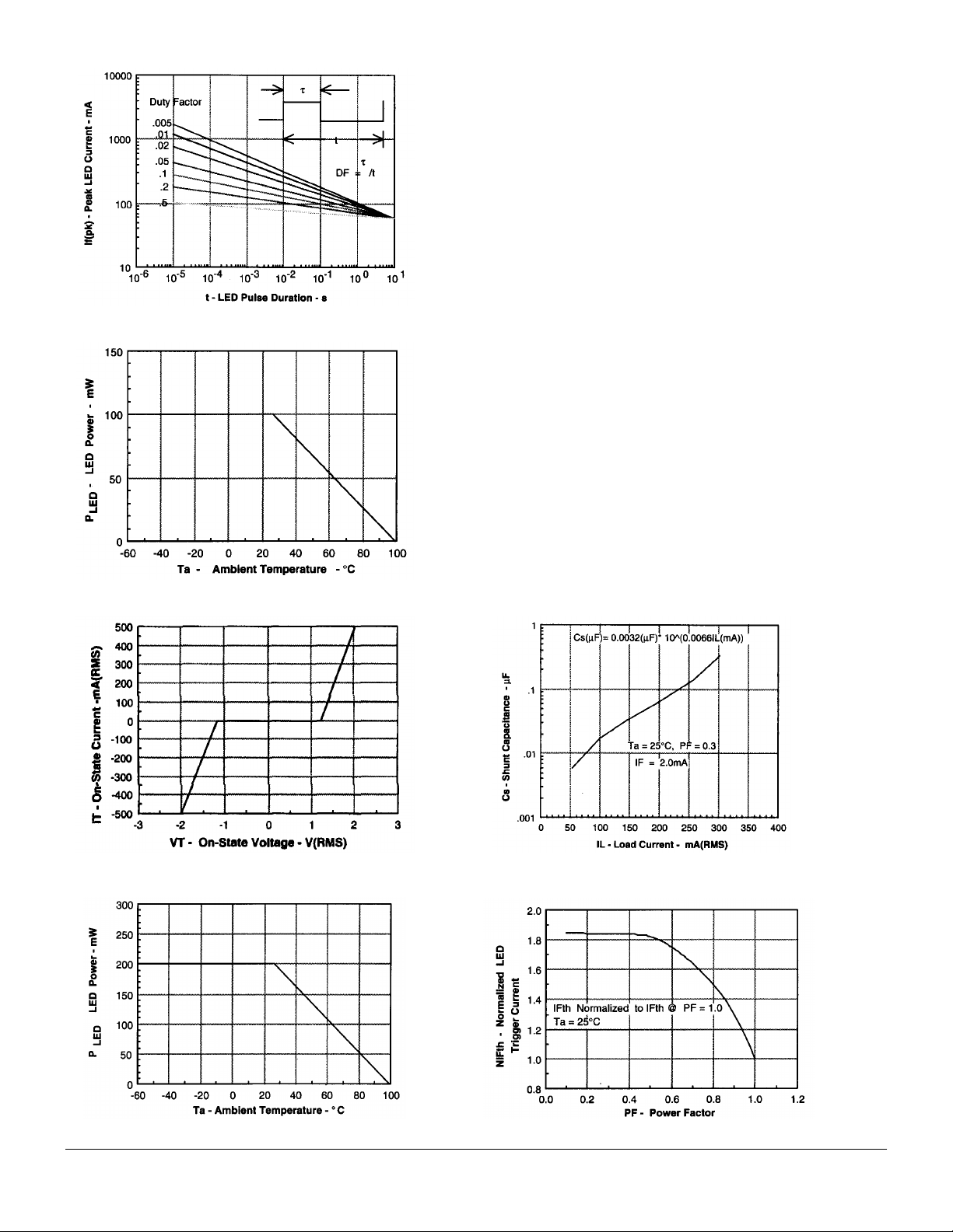
Figure 3. Peak LED current vs. duty factor, Tau
Figure 4. Maximum LED power dissipation
Power Factor Considerations
A snubber isn’t needed to eliminate false operation of the
TRIAC driver because of the IL411’s high static and commutating dv/dt with loads between 1 and 0.8 power factors. When
inductive loads with power factors less than 0.8 are being
driven, include a RC snubber or a single capacitor directly
across the device to damp the peak commutating dv/dt spike.
Normally a commutating dv/dt causes a turning-off device to
stay on due to the stored energy remaining in the turning-off
device.
But in the case of a zero voltage crossing optotriac, the commutating dv/dt spikes can inhibit one half of the TRIAC from
turning on. If the spike potential exceeds the inhibit voltage of
the zero cross detection circuit, half of the TRIAC will be heldoff and not turn-on. This hold-off condition can be eliminated by
using a snubber or capacitor placed directly across the optotriac as shown in Figure 7. Note that the value of the capacitor
increases as a function of the load current.
The hold-off condition also can be eliminated by providing a
higher level of LED drive current. The higher LED drive provides a larger photocurrent which causer . the phototransistor to
turn-on before the commutating spike has activated the zero
cross network. Figure 8 shows the relationship of the LED drive
for power factors of less than 1.0. The curve shows that if a
device requires 1.5 mA for a resistive load, then 1.8 times (2.7
mA) that amount would be required to control an inductive load
whose power factor is less than 0.3.
Figure 5. On-state terminal voltage vs. terminal current
Figure 6. Maximum output power dissipation
Figure 7. Shunt capacitance versus load current
versus power factor
Figure 8. Normalized LED trigger current
5–3
IL4116/4117/4118
 Loading...