

Page 1
TRANSISTOR PLANT semiconductor technical data
E-mail: [email protected]
IL2931Z-9
IL2931T-9
Chip for low dropout positive voltage regulator IC
Features:
- INPUT-TO-OUTPUT VOLT AGE DIFFERENTIAL OF < 0.6V @ 100mA;
- OUTPUT CURRENT IN EX CESS OF 100 mA;
- LOW BIAS CURRENT;
- 60V LOAD DUMP PROTECTION;
- -50V REVERSE TRANSIENT PROTECTION;
- INTERNAL CURRENT LIMITING WITH THERMAL SHUTDOWN;
IDEALLY SULTED FOR BATTERY POWERED EQUIPMENT
Physical Characteristics:
Wafer Diameter ……100 ± 0.5 mm
Wafer thickness ….. 350 ± 20 µm;
Die size …………….. 2.0 x 1.4 mm2;
Scribe width ………...90 µm
Metallization: Top … Al – 1.4 ± 0.2 µm
bottom... Ti -Ni-Ag
Ti - 0.12 ± 0.02µm
Ni – 0.5 ± 0.1µm
Ag – 0.6 ± 0.1µm
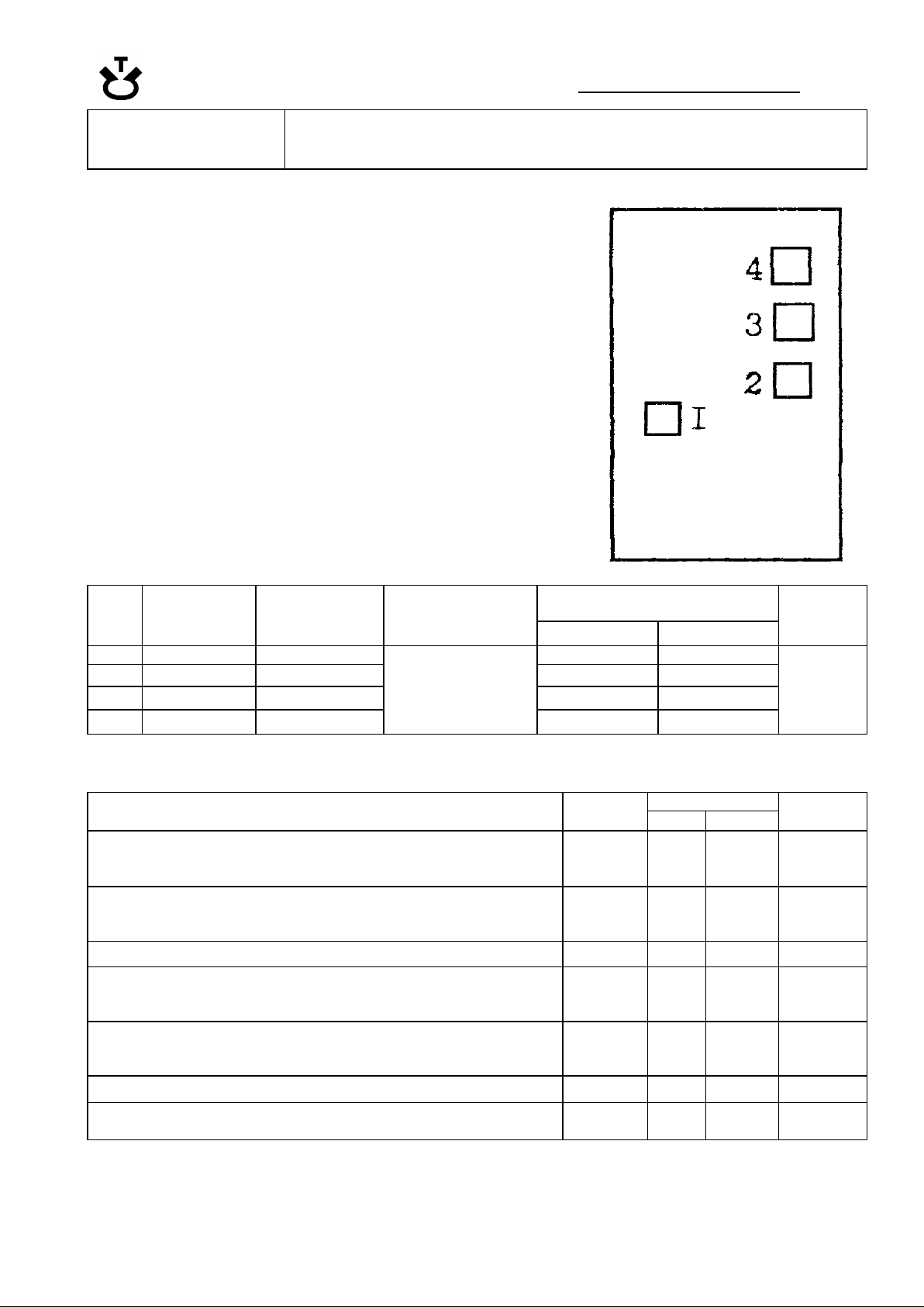
Co-ordinates(bottom left coordinates corner), mm
Pad #
Characteristics
Bond Pad (µm)
Note
X Y
Note
1
output 180 x 180 0.070 0.850
2
GNG 180 x 180 1.085 1.200
3
Input 180 x 180 1.060 1.480
4
Input 180 x 180
- The numbers of
Pads are simulated
When packing Pads 3
and 4 are to be
interconnected
1.060 1.740
Co-ordinates
are given
co-ordinates
on
“metallizatio
n layer”
ELECTRICAL CHARACTERISTICS CHIPS ON WAFER
(Vin=16V,Io=10mA,Ci=0.1ìF,Co=100ìF,Tj=25°C, (Note 1).)
Norm
Characteristic Symbol
Min Max
Unit
Output Voltage
Vin=16V, Io=10mA
Vin=10V to 26V, Io≤100mA
Vo
8.58
8.15
9.43
9.85
V
Line Regulation
Vin=13V to 20V
Vin=10V to 26V
Reg
line
-
-
18
58
mV
Load Regulation (Io=5.0mA to 100mA) Reg
load
- 98 mV
Bias Current
Vin=16V, Io=100mA
Vin=10V to 26V, Io=10mA
IB
-
-
27
0.9
mA
Dropout Voltage
Io=10mA
Io=100mA
VI-Vo
-
-
0.19
0.58
V
Over-Voltage Shutdown Threshold V
th(OV
) 27 39 V
Output Voltage with Reverse Polarity Input
(Vin=-15V)
-Vo
-0.25
-
V
Note 1: Low duty cycle pulse techniques are used during test to maintain junction temperature as to ambient as possible.
 Loading...