

Page 1
IL221AT/IL222AT/IL223AT
PHOTODARLINGTON
SMALL OUTLINE
SURFACE MOUNT OPTOCOUPLER
NEW
FEATURES
• High Current Transfer Ratio, I
IL221AT, 100% Minimum
IL222AT, 200% Minimum
IL223AT, 500% Minimum
• Withstand Test Voltage, 2500 VAC
=1 mA,
F
RMS
• Electrical Specifications Similar to
Standard 6 Pin Coupler
• Industry Standard SOIC-8 Surface
Mountable Package
• Standard Lead Spacing, .05"
• Available in Tape and Reel (suffix T)
(Conforms to EIA Standard RS481A)
• Compatible with Dual Wave, Vapor Phase
and IR Reflow Soldering
• Underwriters Lab File #E52744
(Code Letter P)
DESCRIPTION
The IL221AT/IL222AT/IL223AT is a high current
transfer ratio (CTR) optocoupler with a Gallium
Arsenide infrared LED emitter and a silicon NPN
photodarlington transistor detector.
This device has a CTR tested at an 1 mA LED
current. This low drive current permits easy interfacing from CMOS to LSTTL or TTL.
This optocoupler is constructed in a standard SOIC8 foot print which makes it ideally suited for high
density applications. In addition to eliminating
through-holes requirements, this package conforms
to standards for surface mounted devices.
Maximum Ratings
Emitter
Peak Reverse Voltage............................................ 6.0 V
Continuous Forward Current ...............................60 mA
Power Dissipation at 25°C .................................. 90 mW
Derate Linearly from 25°C ............................ 1.2 mW/°C
Detector
Collector-Emitter Breakdown Voltage ..................... 30 V
Emitter-Collector Breakdown Voltage ....................... 5 V
Collector-Base Breakdown Voltage ........................ 70 V
Power Dissipation ............................................. 150 mW
Derate Linearly from 25°C ........................... 2.0 mW/°C
Package
Total Package Dissipation at 25°C Ambient
(LED + Detector) ........................................... 240 mW
Derate Linearly from 25°C ........................... 3.3 mW/°C
Storage Temperature ......................... – 55°C to +150°C
Operating Temperature ..................... – 55°C to +100°C
Soldering Time at 260°C .................................... 10 sec.
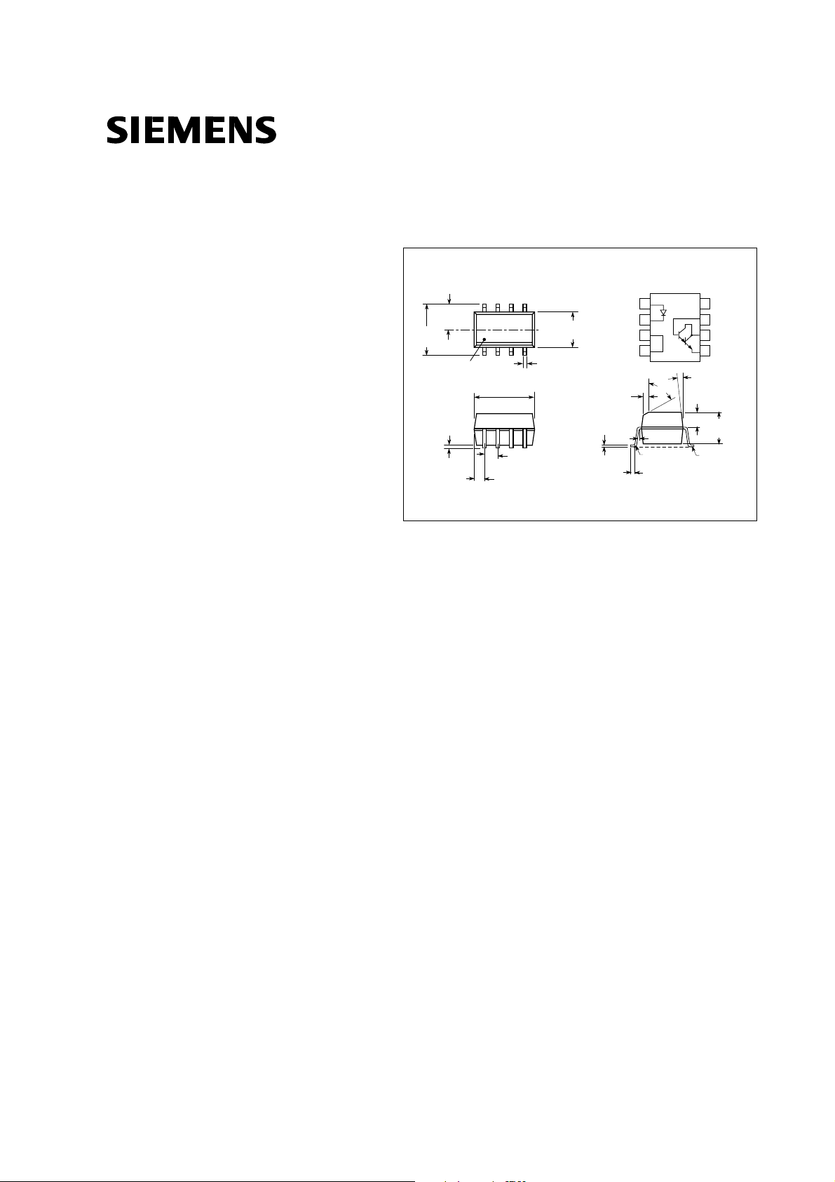
Package Dimensions in Inches (mm)
Anode
.120±.005
(3.05±.13)
.240
(6.10)
.004 (.10)
.008 (.20)
Pin One ID
.192±.005
(4.88±.13)
C
L
.016 (.41)
.050 (1.27)
typ.
.040 (1.02)
.154±.005
(3.91±.13)
.015±.002
(.38±.05)
.008 (.20)
.020±.004
(.15±.10)
2 plcs.
TOLERANCE: ±.005 (unless otherwise noted)
Cathode
NC
NC
1
2
3
4
40°
5° max.
R.010
(.25) max.
7°
.058±.005
(1.49±.13)
Characteristics (TA=25°C)
Emitter
Forward Voltage V
Reverse Current I
Capacitance C
Detector
Breakdown Voltage
Collector-Emitter BV
Emitter-Collector BV
Collector-Base Voltage BV
Collector-Emitter
Capacitance C
Package
DC Current Transfer I
Ratio CTR
IL221AT 100
IL222AT 200
IL223AT 500
Collector-Emitter I
Saturation Voltage V
Isolation Test
Voltage V
Capacitance,
Input to Output C
Resistance,
Input to Output R
Specifications subject to change.
Symbol Min. Typ. Max. Unit Condition
F
R
O
CEO
ECO
CBO
CE
DC
CE sat
IO
IO
IO
1.0 1.5 V IF=1mA
0.1 100 µAV
25 pF VF=0 V,
30 V I
5VI
70 I
3.4 pF VCE=10 V
1VIF=1 mA
2500 VAC
0.5 pF
100 GΩ
RMS
8
NC
7
Base
6
Collector
5
Emitter
.125±.005
(3.18±.13)
Lead
Coplanarity
±.0015 (.04)
max.
=6.0 V
R
F=1 MHz
=100 µA
C
=100 µA
E
=10 µA
C
=1 mA,
F
VCE=5 V
=0.5 mA,
CE
t=1 sec.
Semiconductor Group 4–10
10.95
Page 2
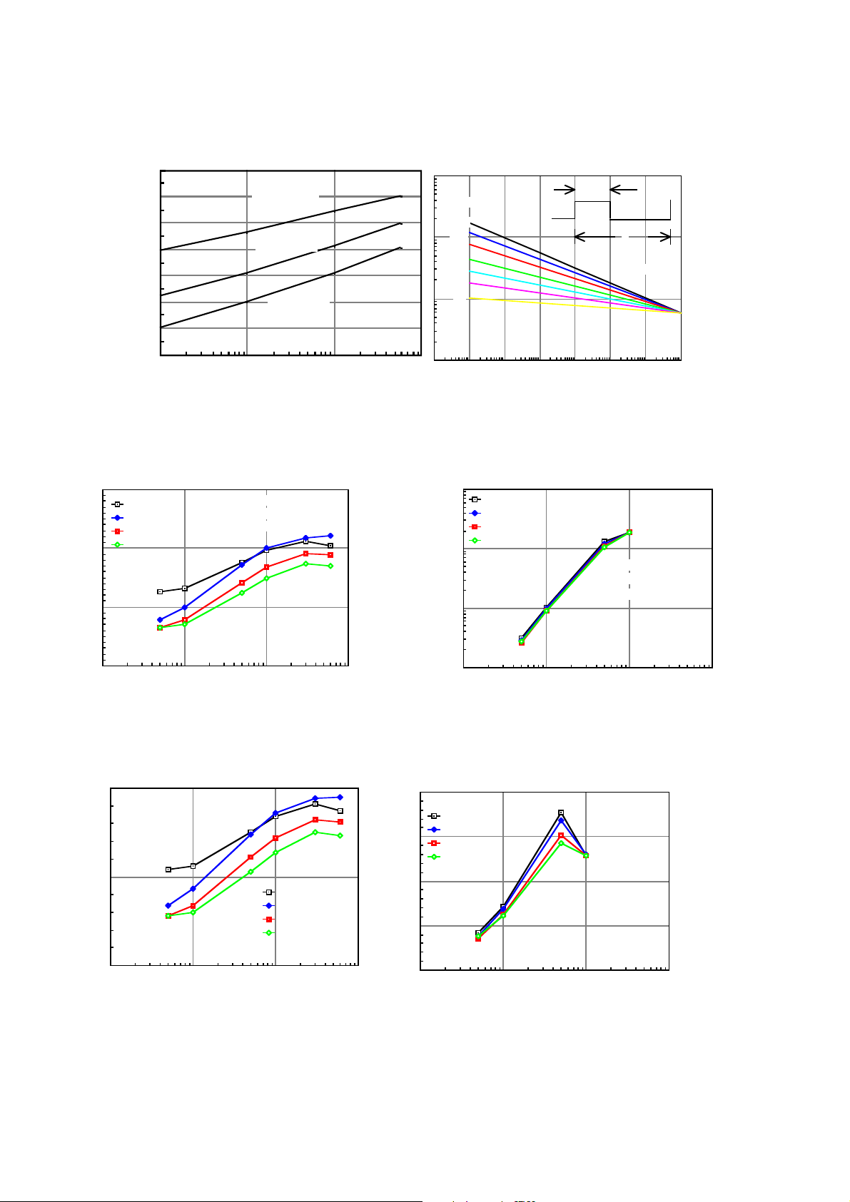
Figure 1. Forward voltage versus forward current Figure 2. Peak LED current versus duty factor, Tau
1.4
1.3
1.2
1.1
1.0
0.9
0.8
VF - Forward Voltage - V
0.7
Figure 3. Normalized CTR
3
Ta = -20°C
Ta = 25°C
Ta = 50°C
Ta =70°C
2
1
Normalized CTRcb
Ta = -55°C
Ta = 25°C
Ta = 85°C
IF - Forward Current - mA
versus I
CB
Normalized to:
If = 1mA, Ta = 25°C
Vcb = 10V
F
10000
Duty Factor
.005
1000
If(pk) - Peak LED Current - mA
100101.1
.01
.02
.05
.1
.2
.5
100
10
10-610-510-410-310-210-110010
t - LED Pulse Duration - s
τ
Figure 4. Normalized CTRCE versus LED current
100
10
Normalized CTRce
Ta = -20°C
Ta = 25°C
Ta = 50°C
Ta = 70°C
1
t
τ
DF = /t
1
Normalized to:
If = 1mA, Vce = 5V
Ta = 25°C
= τ/t
0
.1 1 10 100
If - LED Current - mA
Figure 5. CTR
0.10
versus LED current Figure 6. CTR versus LED current
CB
VCB =10 V
0.05
Ta = -20°C
If/Icb - CTRcb - %
0.00
.1 1 10 100
If - LED Current - mA
Ta = 25°C
Ta = 50°C
Ta = 70°C
.1
.1 1 10 100
If - LED Current - mA
2000
Ta = -20°C
1500
1000
500
CTRce - Current Transfer Ratio -%
Ta = 25°C
Ta = 50°C
Ta = 70°C
0
.1 1 10 100
If - LED Current - mA
Vce = 10V
Semiconductor Group 4–11
Page 3
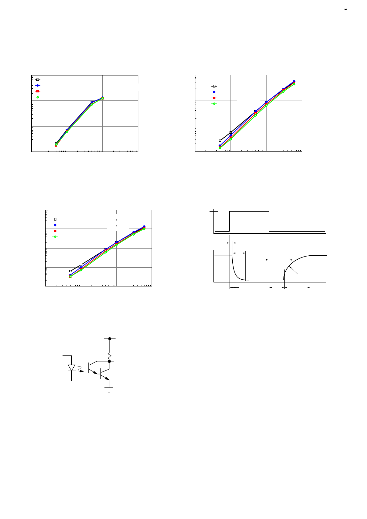
Figure 7. Collector current versus LED current Figure 8. Photocurrent versus LED current
y
1000
100
10
Ice - Collector Current - mA
Ta -20°C
Ta = 25°C
Ta = 50°C
Ta = 70°C
1
.1 1 10 100
Figure 9. Normalized ICB versus I
1000
100
10
Normalized Icb
1
Ta = 20°C
Ta = 25°C
Ta = 50°C
Ta = 70°C
If - LED Current - mA
Ta = -20°C
Ta = 25°C
Ta = 50°C
Ta =70°C
Vce = 10V
Normalized to:
IF = 1mA, Ta =25°C
Vcb = 10V
F
Vce = 5V
100
Ta = 20°C
Icb-20°C
Ta = 25°C
Icb 25°C
Ta = 50°C
10
1
Icb - Photocurrent - µA
.1
.1 1 10 100
V
Icb 50°C
Ta = 70°C
Icb 70°C
If - LED Current - mA
Figure 10. Switching Timing
I
F
t
D
t
O
R
t
PLH
.1
.1 1 10 100
If - LED Current - mA
Figure 11. Switching schematic
VCC=10 V
F=10 KHz,
DF=50%
IF=5 mA
R
L
V
O
t
PHL
VTH=1.5 V
t
S
t
F
Semiconductor Group 4–12
 Loading...