

Page 1

Semiconductor
IH6201
OBSOLETE PRODUCT
April 1999
NO RECOMMENDED REPLACEMENT
Call Central Applications 1-800-442-7747
or email: [email protected]
Features
• Driven Direct from TTL or CMOS Logic
• Translates Logic Levels Up to 30V Levels
• Switches 20V
Signals When Used in Conjunction
ACPP
with the IH401A Varafet (As An Analog Gate)
•t
≤ 300ns & t
ON
≤ 200ns for 30V Level Shifts
OFF
• Quiescent Supply Current ≤ 100µA for Any State (DC)
• Provides Both Normal & Inverted Outputs
Part Number Information
TEMP. RANGE
PART NUMBER
IH6201CJE 0 to 70 16 Ld CerDIP
IH6201MJE -55 to 125 16 Ld CerDIP
IH6201CPE 0 to 70 16 Ld PDIP
(oC) PACKAGE
Dual CMOS
Driver/Voltage Translator
Description
The IH6201 is a CMOS, Monolithic, Dual Voltage Translator;
it takes low level TTL or CMOS logic signals and converts
them to higher levels (i.e. to ±15V swings). This translator is
typically used in making solid state switches, or analog
gates.
When used in conjunction with the IH401A Varafets, the
combination makes a complete solid state switch capable of
switching signals up to 22V
frequency. This switch is a “break-before-make” type (i.e.
t
time < tON time). The combination has typical t
OFF
80ns and typical t
≈ 200ns for signals up to 20V
ON
amplitude.
A TTL “1” input strobe will force the θ driver output up to V+
level; the
θ output will be driven down to the V- level. When
the TTL input goes to “0”, the θ output goes to V- and
to V+; thus θ and
θ are 180o out of phase with each other.
These complementary outputs can be used to create a wide
variety of functions such as SPDT and DPDT switches, etc.;
alternatively the complementary outputs can be used to
drive N and P channel MOSFETs, to make a complete
CMOS analog gate.
and up to 20MHz in
P-P
OFF
in
P-P
θ goes
≈
Pinout
IH6201
(OUTLINE DWGS, JE, PE)
TOP VIEW
16
15
14
13
12
11
10
9
NC
NC
NC
NC
1
θ1
2
3
4
θ1
5
θ2
6
7
8
θ2
The driver typically uses +5V and ±15V power supplies,
howev er a wide r ange of V+ and V- is also possible. It is necessary that V+ > 5V for the driver to work properly, however.
Functional Diagram
NC
TTL INPUT 1
VGND
+5V
V+
TTL INPUT 2
NC
CAUTION: These devices are sensitive to electrostatic discharge. Users should follow proper IC Handling Procedures.
Copyright
© Harris Corporation 1998
4-1
File Number 3136.2
Page 2

IH6201
Absolute Maximum Ratings Thermal Information
Supply Voltage (V+ to V-) . . . . . . . . . . . . . . . . . . . . . . . . . . . . . . 35V
V+. . . . . . . . . . . . . . . . . . . . . . . . . . . . . . . . . . . . . . . . . . . . . . . . 35V
V- . . . . . . . . . . . . . . . . . . . . . . . . . . . . . . . . . . . . . . . . . . . . . . . . 35V
V+ to VIN . . . . . . . . . . . . . . . . . . . . . . . . . . . . . . . . . . . . . . . . . . 40V
Operating Conditions
Temperature Range . . . . . . . . . . . . . . . . . . . . . . . . . -55oC to 125oC
CAUTION: Stresses above those listed in “Absolute Maxim um Ratings” ma y cause permanent damage to the device . This is a stress only rating and oper ation of
the device at these or any other conditions above those indicated in the operational sections of this specification is not implied.
Storage Temperature Range. . . . . . . . . . . . . . . . . . .-65oC to 150oC
Lead Temperature (Soldering, 10s). . . . . . . . . . . . . . . . . . . . . 300oC
Electrical Specifications V+ = +15V, V- = -15V, V
PARAMETER TEST CONDITIONS
θ or θ Driver Output Swing VIN = 0V + 3V, Figure 3B - 28 - - 28 - V
VIN Strobe Level (“1”) for
Proper Translation
VIN Strobe Level (“0”) for
Proper Translation
IIN Input Strobe Current
Draw (for 0V - 5V Range)
tON Time VIN = 0V CL = 30pF Switching
t
Time VIN = 0V CL= 30pF Switching
OFF
I+ (V+) Power Supply
Quiescent Current
I- (V-) Power Supply
Quiescent Current
IL (VL) Power Supply
Quiescent Current
θ≥ 14V, θ≥ -14V 3.0 3.0 3.0 - 2.4 - V
θ≥ -14V, θ≥ 14V 0.4 0.4 0.4 - 0.8 - V
VIN = 0V or +5V ±1 ±110±1 ±110µA
Turn-on Time, Figure 3B
Turn-off Time, Figure 3B
VIN = 0V or +5V 100 100 100 100 100 100 µA
VIN = 0V or +5V 100 100 100 100 100 100 µA
VIN = 0V or +5V 100 100 100 100 100 100 µA
= +5V
L
IH6201CJE, CPE IH6201MJE
- 500 - - 500 - ns
- 500 - - 500 - ns
UNITS0oC25oC70oC -55oC25oC 125oC
P-P
DC
DC
4-2
Page 3
Schematic Diagram
IH6201
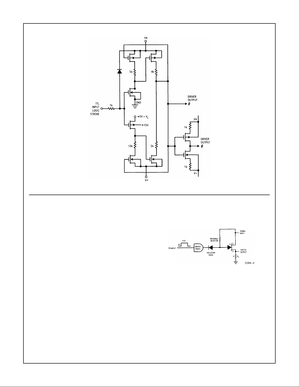
FIGURE 1. SCHEMATIC DIAGRAM (ONE CHANNEL)
Applications
Input Drive Capability
The strobe input lines are designed to be driven from TTL
logic levels; this means 0.8V to 2.4V levels max. and min.
respectively. For those users who require 0.8V to 2.0V
operation, a pull-up resistor is recommended from the TTL
output to +5V line. This resister is not critical and can be in
the 1kΩ to 10kΩ range.
When using 4000 series CMOS logic, the input strobe is
connected direct to the 4000 series gate output and no pull
up resistors, or any other interface is necessary.
When the input strobe voltage level goes below GND (i.e. to
-15V) the circuit is unaffected as long as V+ to V
exceed absolute maximum rating.
Output Drive Capability
The translator output is designed to drive the IH401A
Varafets; these are N-channel JFETS with built-in driver
diodes. Driver diodes are necessary to isolate the signal
source from the driver/translator output; this prevents a
forward bias condition between the signal input and the
+V
supply. The IH6201 will drive any JFET provided some
CC
sort of isolation is added.
You will notice in Figure 2 that a “referral” resistor has been
added from 2N4391 gate to its source. This resistor is
needed to compensate for the inadequate charge area curve
for isolation diode i.e. if C vs. V plot f or diode≤ 2 [C vs . V plot
does not
IN
for output JFET] switch won’t function; then adding this
resistor overcomes this condition. The “referral” resistor is
normally in the 100kΩ to 1MΩ range and is not tool critical.
FIGURE 2.
Making a Complete Solid State Switch that Can Handle
20V
Signals
P-P
The limitation on signal handling capability comes from the
output gating device. When a JFET is used, the pinch-off of
the JFET acting with the V- supply does the limiting. In fact
max. signal handling capability = 2 (V
+ (V-)) V
P
P-P
where V
= pinch-off voltage of JFET chosen. i.e. VP = 7V, V- = -15V:
max. signal handling = 2(7V + (-15V)) V
= 2(-8V
P-P
) = 16V
. Obviously to get ≥ 20V
P-P
with V- = -15V. Another simple way to get 20V
= 2 (7V - 15) V
P-P
P-P
, VP≥ 5V
P-P
with VP =
P-P
7V, is to increase V- to -17V. In fact using V+ = +12V or +15V
and setting V- = -18V allows one to switch 20V
IH401A. The advantage of using the V
with unsymmetrical supplies), over the V
= 7V pinch-off (along
P
= 5V pinch-off (and
P
with the
P-P
P
4-3
Page 4
IH6201
±15V supplies), is that you will have a m uch lower R
the V
= 7 JFET (i.e. for the 2N4391).
P
r
DS(ON)
V
≈ 22Ω,R
= 7V VP = 5V
P
DS(ON)
≈ 35Ω
DS(ON)
for
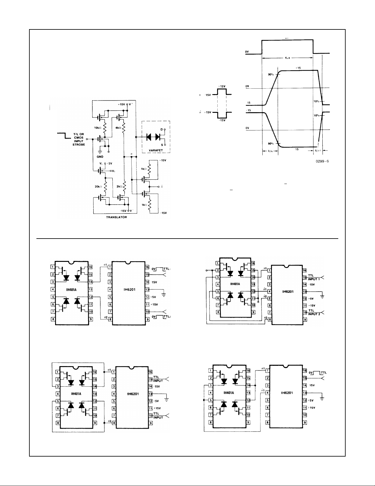
The IH6201 is a dual translator, each containing 4 CMOS
FET pairs. The schematic of one-half of an IH6201, driving
one-quarter of an IH401A, is shown in Figure 3A.
FIGURE 3A.
FIGURE 3B.
NOTE: Each translator output has a θ and θ output, θ is just the
inverse of θ.
A very useful feature of this system is that one-half of an
IH6201 and one-half of an IH401A can combine to make a
SPDT switch, or an IH6201 plus an IH401A can make a dual
SPDT analog switch (See Figure 6).
Switches
FIGURE 4. DUAL SPST ANALOG SWITCH FIGURE 5. DPDT ANALOG SWITCH
FIGURE 6. DUAL SPDT FIGURE 7. DUAL DPST
4-4
 Loading...