

Page 1
Semiconductor
IH6108
OBSOLETE PRODUCT
April 1999
POSSIBLE SUBSTITUTE PRODUCT
DG408, DG508A, HI-0508(A)
Features
• Ultra Low Leakage - I
•r
< 400Ω Over Full Signal and Temperature
DS(ON)
Range
• Power Supply Quiescent Current Less Than 100µA
• ±14V Analog Signal Range
• No SCR Latchup
• Break-Before-Make Switching
• Binary Address Control (3 Address Inputs Control 8
Channels)
• TTL and CMOS Compatible Strobe Control
• Pin Compatible with DG508A, HI-508 and ADG508A
• Internal Diode in Series with V+ for Fault Protection
D(OFF)
≤ 100pA (Typ)
8-Channel
CMOS Analog Multiplexer
Description
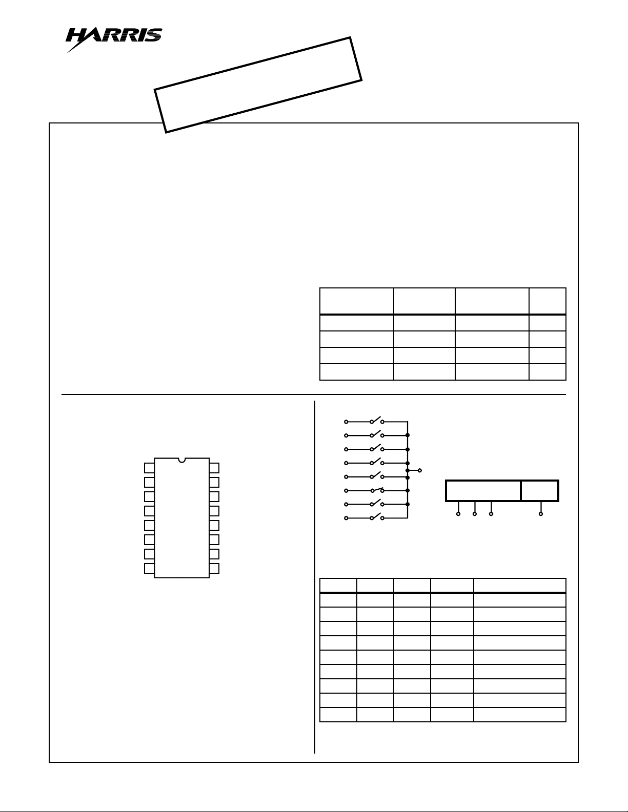
The IH6108 is a CMOS 1-of-8 multiplexer. The part is a plugin replacement for the DG508A. Three-line decoding is used
so that the 8 channels can be controlled by 3 Address
inputs; additionally a fourth input is provided for use as a
system enable. When the ENABLE input is high (5V), a
channel is selected by the three Address inputs, and when
low (0V) all channels are off. The 3 Address inputs are TTL
and CMOS logic compatible, with a “1” corresponding to any
voltage greater than 2.4V.
Part Number Information
PART
NUMBER
IH6108MJE -55 to 125 16 Ld CERDIP F16.3
IH6108MJE/883B -55 to 125 16 Ld CERDIP F16.3
IH6108CJE 0 to 70 16 Ld CERDIP F16.3
IH6108CPE 0 to 70 16 Ld PDIP E16.3
TEMP.
RANGE (oC) PACKAGE
PKG.
NO.
Pinout
(CERDIP, PDIP)
1
A
0
2
EN
3
V-
S
4
1
5
S
2
6
S
3
7
S
4
8
D
IH6108
TOP VIEW
Functional Diagram
S
1
S
2
S
3
S
16
A
1
15
A
2
14
GND
V+
13
12
S
5
11
S
6
10
S
7
9
S
8
4
S
5
S
6
S
7
S
8
A
2
x x x 0 None
000 1 1
001 1 2
010 1 3
011 1 4
100 1 5
101 1 6
110 1 7
111 1 8
NOTE: A0, A1, A
A
1
Logic “1” = VAH≥ 2.4V, V
Logic “0” = VAL≤ 0.8V.
2
V
OUT
D
3 LINE BINARY ADDRESS INPUT
TRUTH TABLE
A
0
EN ON SWITCH
ENH
ADDRESS DECODER
1 OF 8
A0A1A
ABOVE EXAMPLE SHOWS
CHANNEL 6 TURNED ON.
≥ 4.5V
2
(1 0 1) AND EN AT 5V
ENABLE
INPUT
EN
CAUTION: These devices are sensitive to electrostatic discharge. Users should follow proper IC Handling Procedures.
Copyright
© Harris Corporation 1997
12-128
File Number 3156.2
Page 2
IH6108
Absolute Maximum Ratings Thermal Information
VIN (A, EN) to Ground . . . . . . . . . . . . . . . . . . . . . . . . . . -15V to 15V
VS or VD to V+ . . . . . . . . . . . . . . . . . . . . . . . . . . . . . . . . . . .0V, -36V
VS to VD to V-. . . . . . . . . . . . . . . . . . . . . . . . . . . . . . . . . . . . 0V, 36V
V+ to Ground . . . . . . . . . . . . . . . . . . . . . . . . . . . . . . . . . . . . . . . 18V
V- to Ground. . . . . . . . . . . . . . . . . . . . . . . . . . . . . . . . . . . . . . . .-18V
Current (Any Terminal) . . . . . . . . . . . . . . . . . . . . . . . . . . . . . . 30mA
Current (Analog Source or Drain) . . . . . . . . . . . . . . . . . . . . . .20mA
Operating Conditions
Temperature Range
C Suffix . . . . . . . . . . . . . . . . . . . . . . . . . . . . . . . . . . . .0oC to 70oC
M Suffix. . . . . . . . . . . . . . . . . . . . . . . . . . . . . . . . .-55oC to 125oC
CAUTION: Stresses above those listed in “Absolute Maximum Ratings” may cause permanent damage to the device. This is a stress only rating and operation
of the device at these or any other conditions above those indicated in the operational sections of this specification is not implied.
NOTE:
1. θJA is measured with the component mounted on an evaluation PC board in free air.
CAUTION: Stresses above those listed in “Absolute Maxim um Ratings” ma y cause permanent damage to the device . This is a stress only rating and oper ation of
the device at these or any other conditions above those indicated in the operational sections of this specification is not implied.
Thermal Resistance (Typical, Note 1) θJA (oC/W) θJC (oC/W)
PDIP Package. . . . . . . . . . . . . . . . . . . 100 N/A
CERDIP Package . . . . . . . . . . . . . . . . 75 20
Maximum Junction Temperature (Hermetic Package) . . . . . . . .175oC
Maximum Junction Temperature (Plastic Package) . . . . . . . . 150oC
Maximum Storage Temperature Range . . . . . . . . . .-65oC to 150oC
Maximum Lead Temperature (Soldering 10s). . . . . . . . . . . . . 300oC
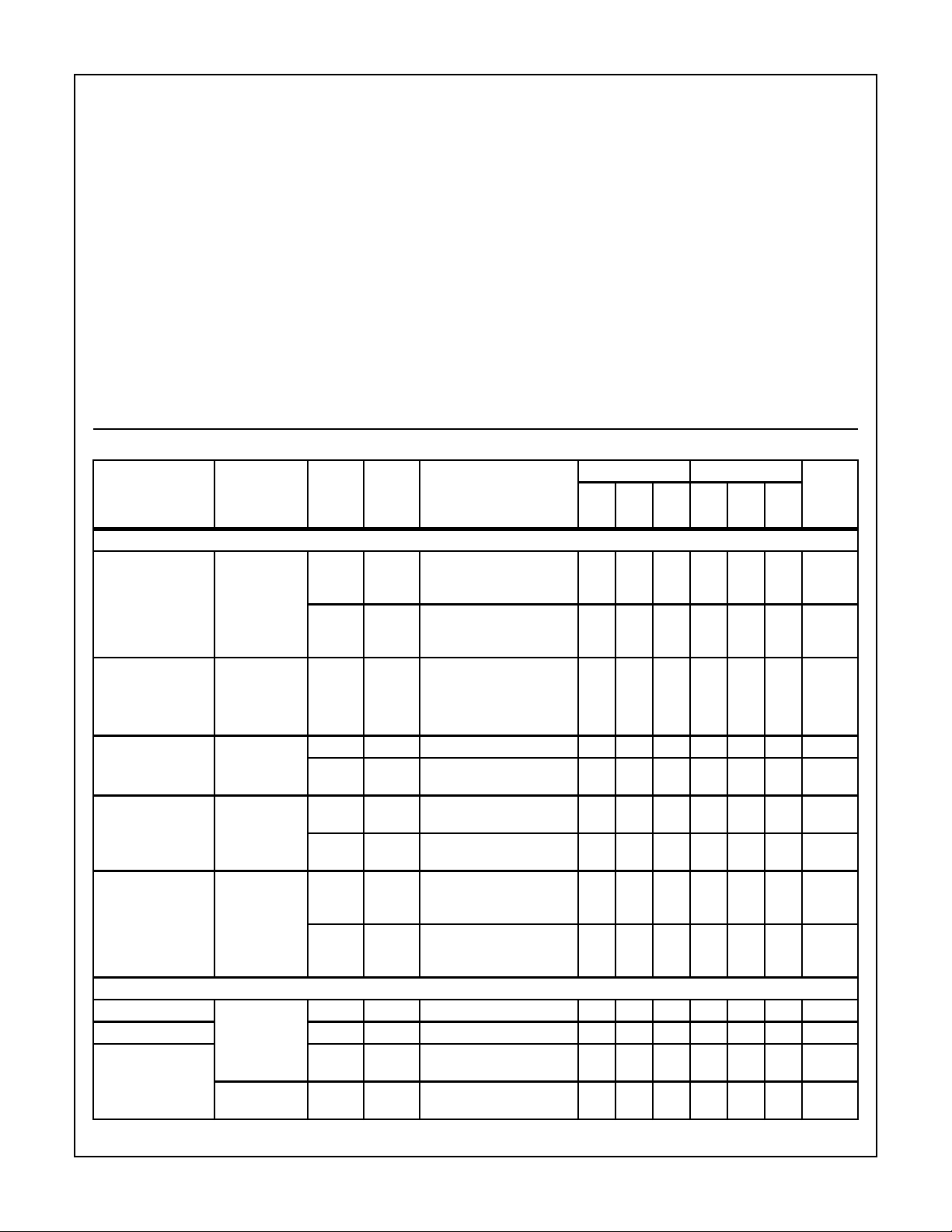
Electrical Specifications V+ = 15V, V- = -15V, V
NO
TESTS
PARAMETER
SWITCH
r
DS(ON)
∆r
DS(ON)
I
S(OFF)
I
D(OFF)
I
D(ON)
INPUT
I
or I
AN(ON)
I
AN(OFF)IA(off)
I
A
A(on)
MEASURED
TERMINAL
S to D 8 180 VD= +10V, IS = -1.0mA
S 8 0.002 VS = 10V, VD = -10V - ±0.5 ±50 - ±1 ±50 nA
D 1 0.03 VD = 10V, VS = -10V,
D 8 0.1 V
A0, A1, or A
Inputs
A0, A1, A
EN 1 0.01 V
PER
TEMP
TYP
25oC TEST CONDITIONS
8 150 V
20 ∆r
8 0.002 V
1 0.03 V
8 0.1 V
3 0.01 VA = 0V - -10 -30 - -10 -30 µA
2
2
3 0.01 VA = 14V - 10 30 - 10 30 µA
3 0.01 VEN = 5V, All VA = 0V
= +5V, Ground = 0V, Unless Otherwise Specified, (Note 4)
EN
M SUFFIX (oC) C SUFFIX (oC)
300 300 400 350 350 450 Ω
Sequence Each Switch On
VAL = 0.8V, VAH = 2.4V
= -10V, IS = -1.0mA
D
300 300 400 350 350 450 Ω
Sequence Each Switch On
VAL = 0.8V, VAH = 2.4V
=
DS(ON)
r
DS ON()MAXrDS ON()MIN
---------------------------------------------------------------------------------- -
–
r
DS ON()AVG
˙
------ %
,
VS = ±10V
= -10V, VD = 10V,
S
- ±0.5 ±50 - ±1 ±50 nA
VEN = 0.8V
- ±2 ±100 - ±5 ±100 nA
VEN = 0.8V
= -10V, VS = 10V,
D
- ±2 ±100 - ±5 ±100 nA
VEN = 0.8V
S(ALL)
= VD = 10V,
- ±2 ±100 - ±5 ±100 nA
Sequence Each Switch On
VAL = 0.8V, VAH = 2.4V
S(ALL)
= VD = -10V,
- ±2 ±100 - ±5 ±100 nA
Sequence Each Switch On
VAL = 0.8V, VAH = 2.4V
- -10 -30 - -10 -30 µA
(Address Pins)
= 0V, All VA = 0V
EN
- -10 -30 - -10 -30 µA
(Address Pins)
UNITS-55 25 125 0 25 70
12-129
Page 3
IH6108
Electrical Specifications V+ = 15V, V- = -15V, V
EN
NO
TESTS
PARAMETER
MEASURED
TERMINAL
PER
TEMP
TYP
25oC TEST CONDITIONS
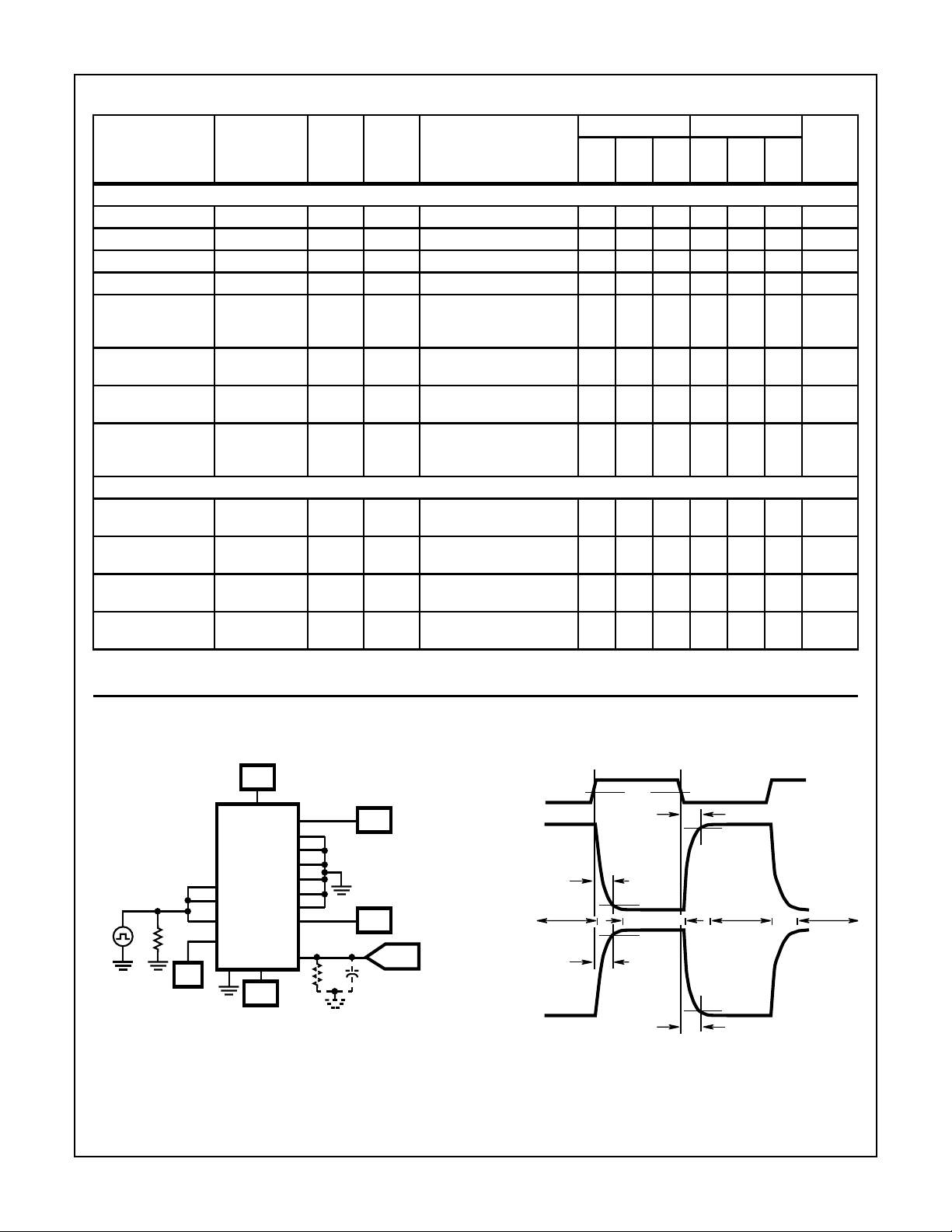
DYNAMIC
t
TRANSITION
t
OPEN
t
ON(EN)
t
OFF(EN)
D 0.3 See Figure 1 - 1 ---- µs
D 0.2 See Figure 2 ------ µs
D 0.6 See Figure 3 - 1.5 ---- µs
D 0.4 See Figure 3 - 1 ---- µs
“OFF” Isolation D 60 V
C
S(OFF)
C
D(OFF)
C
DS(OFF)
S5V
D25V
D to S 1 VS = 0V, VD = 0V,
SUPPLY
Positive Supply
V+ 1 40 V
Current
Negative Supply
V- 1 2 V
Current
Positive Standby
V+ 1 1 V
Current
Negative Standby
V- 1 1 V
Current
NOTE:
2. See “Enable Input Strobing Levels”, in Application Section.
= +5V, Ground = 0V, Unless Otherwise Specified, (Note 4) (Continued)
M SUFFIX (oC) C SUFFIX (oC)
= 0V, RL = 200Ω,
EN
CL = 3pF, VS = 3V
RMS
------ dB
,
f = 500kHz
= 0V, VEN = 0V,
S
------ pF
f = 140kHz to 1MHz
= 0V,VEN= 0V,
D
------ pF
f = 140kHz to 1MHz
------ pF
VEN = 0V,
f = 140kHz to 1MHz
EN
= 5V,
- - 200 - - 1000 µA
All VA = 0V or 5V
EN
= 5V,
- - 100 - - 1000 µA
All VA = 0V or 5V
EN
= 0V,
- - 100 - - 1000 µA
All VA = 0V or 5V
EN
= 0V,
- - 100 - - 1000 µA
All VA = 0V or 5V
UNITS-55 25 125 0 25 70
Switching Information
+15V
V+
IH6108
A
0
A
1
A
V
A
50Ω
+5V
2
EN
V-GND
-15V
FIGURE 1. t
+10V
-10V
3V
50%0.8V
t
trans
S8 ON
t
trans
-9V
+9V
(1-8)
(1-8)
-10V
+10V
t
trans
+9V
S1 ON
-9V
t
trans
(8-1)
S8 ON
(8-1)
V
A
tr < 100ns
tf < 100ns
S
1
S
2
S
3
S
4
S
5
S
6
S
7
S
8
V
OUT
D
±10V
±10V
C
R
P
P
PROBE IMPEDANCE
TRANSITION
V
OUT
VS1 = +10V
VS8 = -10V
S1 ON
PROBE
V
OUT
VS1 = -10V
V
= +10V
R
P
C
P
≥ 1MΩ
≤ 30pF
S8
SWITCHING TEST CIRCUIT AND WAVEFORMS
12-130
Page 4
IH6108
Switching Information
A
2
A
1
THRU
A
0
V
A
+5V
V
EN
IH6108
EN
GND
-15V
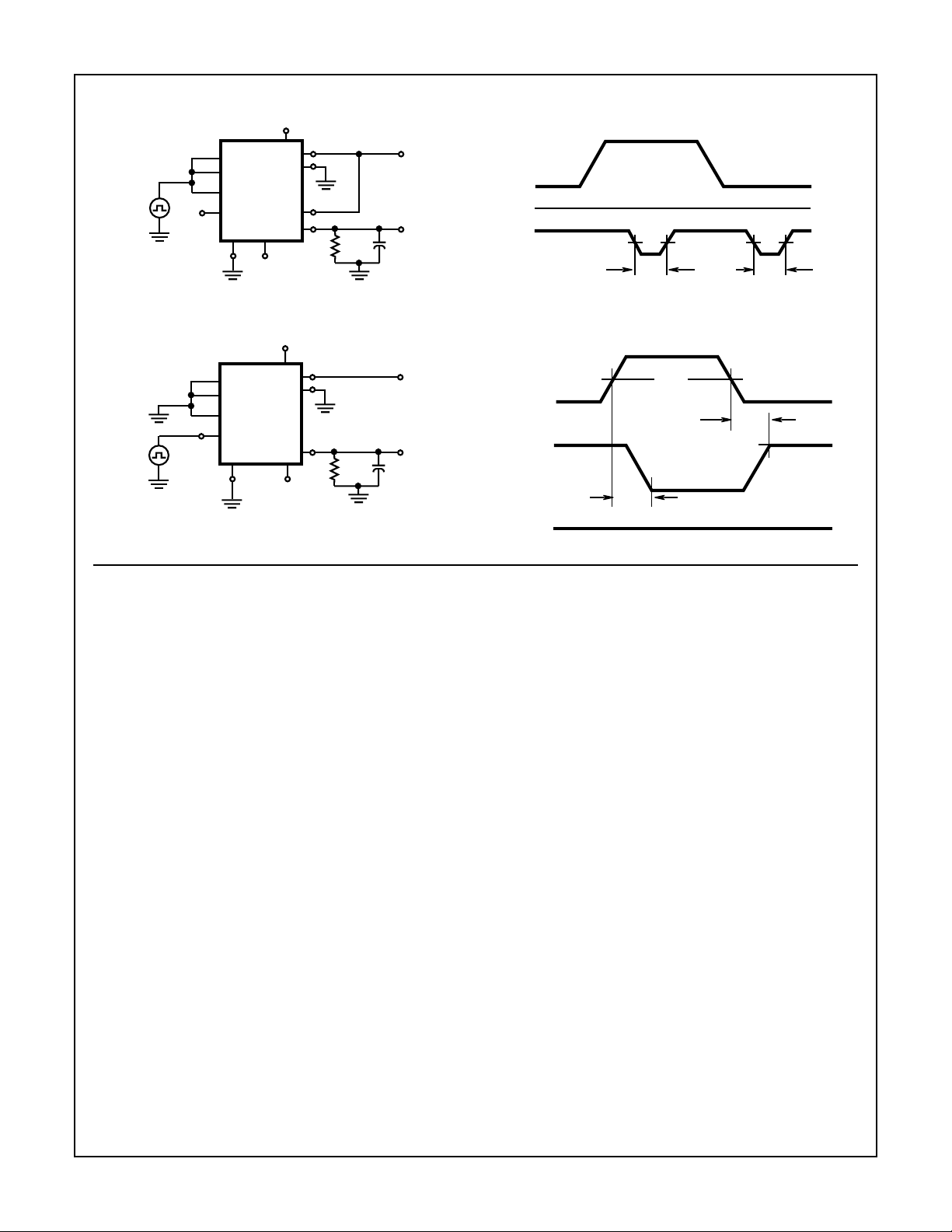
FIGURE 2. t
A
2
A
1
A
0
IH6108
EN
GND
V-
+15V
THRU
-15V
FIGURE 3. tON AND t
(Continued)
+15V
V
S
1
S
2
S
7
S
8
D
OPEN
S
1
S
2
S
8
200Ω
(BREAK-BEFORE-MAKE) SWITCHING TEST CIRCUIT AND WAVEFORMS
OUT
1kΩ
-2V
V
OUT
35pF
V
S1
V
OUT
35pF
SWITCHING TEST CIRCUIT AND WAVEFORMS
OFF
A
tr < 100ns
t
< 100ns
f
V
OUT
V
EN
tr < 100ns
t
< 100ns
f
0.8V
VS1 = -2V
S1 ON S8 ON
t
OPEN
0.8V
V
OUT
0V
t
EN(ON)
VS1 = -2V
3V
50% 50%
50%
90%
5V
t
OPEN
10%
0.8V
t
EN(OFF)
IH6108 Application Information
ENABLE Input Strobing Levels
The ENABLE input on the IH6108 requires a minimum of
+4.5V to trigger to the “1” state and a maximum of +0.8V to
trigger to the “0” state. If the ENABLE input is being driven
from TTL logic, a pull-up resistor of 1k to 3kΩ is required
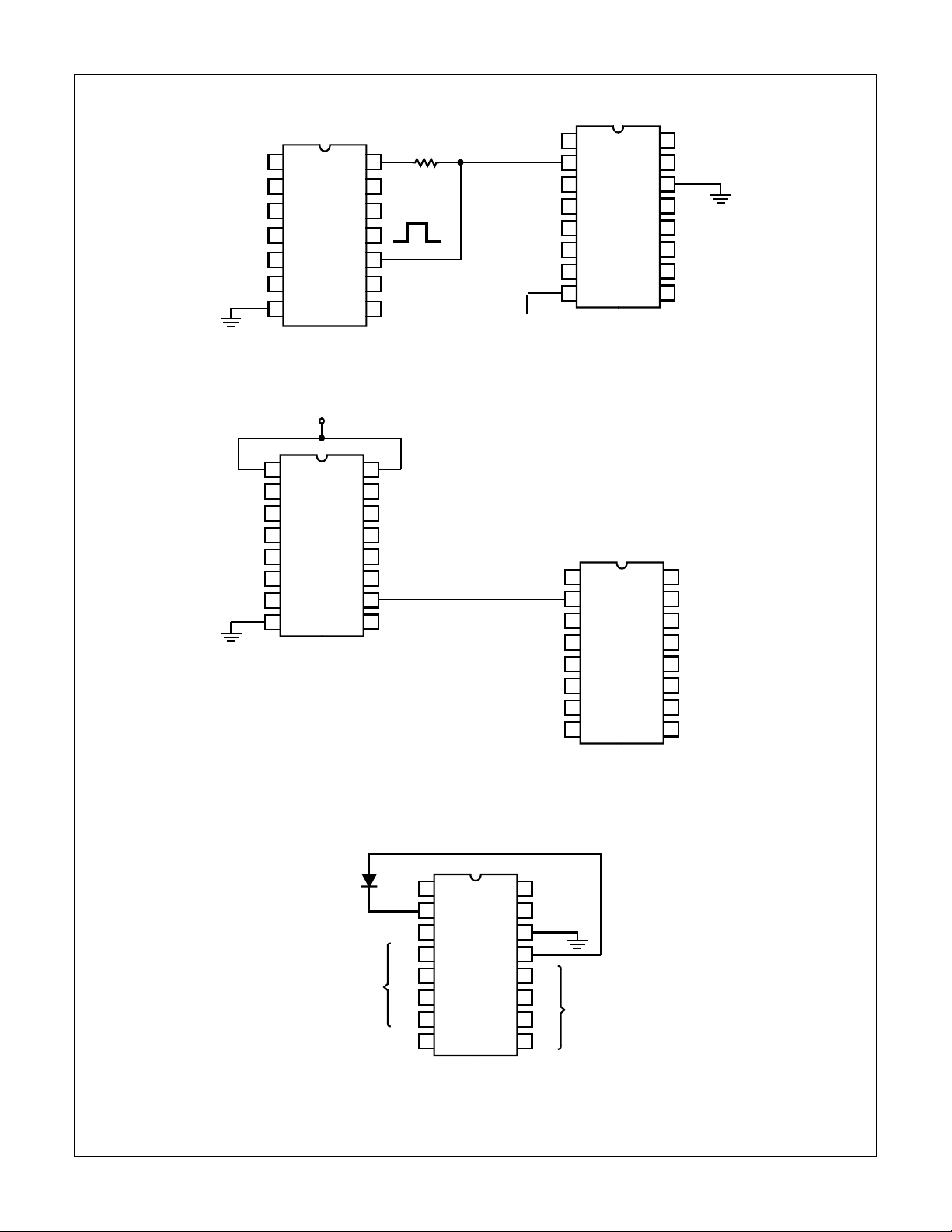
from the gate output to +5V supply. (See Figure 4.)
When the EN input is driven from CMOS logic, no pullup is
necessary, see Figure 5.
The supply voltage of the CD4009 affects the switching
speed of the IH6108; the same is true for TTL supply voltage
levels. The following chart shows the effect, on t
supply varying from +4.5V to +5.5V.
CMOS OR TTL
SUPPLY VOLTAGE
TYPICAL T
AT 25oC
+4.5V 400ns
+4.75V 300ns
+5.00V 250ns
+5.25V 200ns
+5.50V 175ns
The throughput rate can therefore be maximized by using a
+5V to +5.5V supply for the ENABLE Strobe Logic.
The examples shown in Figures 4 and 5 deal with ENABLE
strobing when expansion to more than eight channels is
required. In these cases the EN terminal acts as a fourth
address input. If eight channels or less are being multiplexed, the EN terminal can be directly connected to +5V
logic supply to enable the IH6108 at all times.
trans
TRANS
for a
Using the IH6108 with Supplies Other Than ±15V
The IH6108 can be used with power supplies ranging from
±6V to ±16V. The switch r
will increase as the supply
DS(ON)
voltages decrease, however, the multiplexer error term (the
product of leakage times r
) will remain approximately
DS(ON)
constant since leakage decreases as the supply voltages
are reduced.
Caution must be taken to ensure that the enable (EN)
voltage is at least 0.7V below V+ at all times. If this is not
done, the Address input strobing levels will not function
properly. This may be achieved quite simply by connecting
EN (pin 2) to V+ (pin 13) via a silicon diode as shown in
Figure 6. When using this type of configuration, a further
requirement must be met: the strobe levels of A0 and A1
must be within 2.5V of the EN voltage in order to define a
binary “1” state. For the case shown in Figure 6 the EN voltage is 11.3V which means that logic high at A0 and A1 is
+8.8V (logic low continues to be 0.8V). In this configuration
the IH6108 cannot be driven by TTL (+5V) or CMOS (+5V)
logic. It can be driven by TTL open collector logic or CMOS
logic with +12V supplies.
If the logic and the IH6108 have common supplies, the EN
pin should again be connected to the supply through a
silicon diode. In this case, tying EN to the logic supply
directly will not work since it violates the 0.7V differential
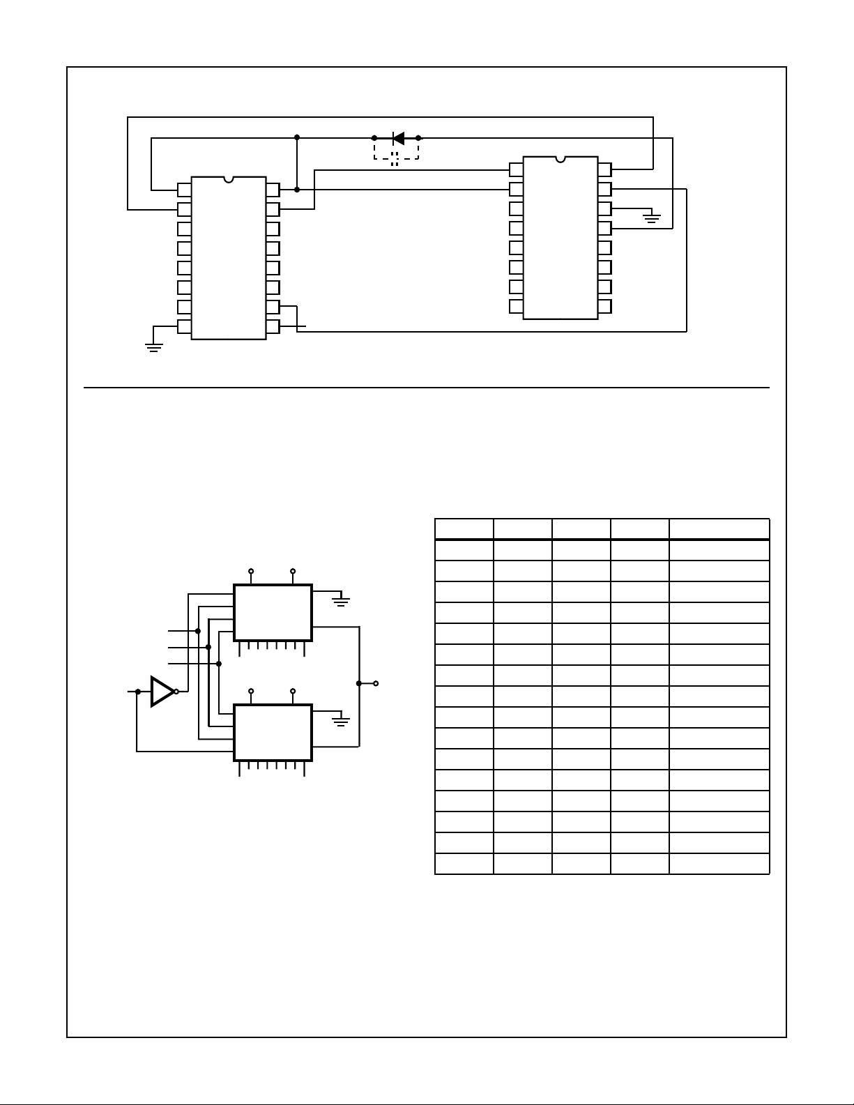
voltage required between V+ and EN, (See Figure 7). A 1µF
capacitor can be placed across the diode to minimize
switching glitches.
12-131
Page 5
Switching Information
1
2
3
4
5
6
7
IH6108
A
0
OUT
EN
-15V
S
S
S
S
1
2
3
4
1
2
3
4
D
IH6108
5
6
7
8
1kΩ
+5V
14
13
12
DM7404N
TTL LOGIC
+3V
0V
11
10
9
8
V
FIGURE 4. ENABLE INPUT STROBING FROM TTL LOGIC
+5V
16
A
1
15
A
2
14
+15V
13
12
S
5
11
S
6
10
S
7
9
S
8
1
2
3
4
CD4009
5
6
7
8
16
15
14
13
12
11
10
9
A
EN
-15V
S
S
S
S
FIGURE 5. ENABLE INPUT DRIVEN FROM CMOS LOGIC
1N914
INPUTS
A
0
1
EN
2
-12V
3
S
4
1
S
2
S
3
S
4
(V
) D
OUT
IH6108
5
6
7
8
16
A
1
15
A
2
14
+12V
13
12
S
5
11
S
6
10
S
7
9
S
8
0
1
2
3
4
D
1
2
3
4
5
6
7
8
INPUTS
IH6108
16
A
1
15
A
2
GND
14
+15V
13
12
S
5
11
S
6
10
S
7
9
S
8
FIGURE 6. IH6108 CONNECTION DIAGRAM FOR LESS THAN ±15V SUPPLY OPERATION
12-132
Page 6
IH6108
Switching Information
1
2
3
4
CD4009A
5
6
7
8
(Continued)
16
15
14
13
12
11
10
9
1N914 OR ANY SILICON DIODE
A
EN
-12V
A
0
1
2
3
4
IH6108
5
6
7
8
16
15
14
13
12
11
10
9
A
+12V
1
2
FIGURE 7. IH6108 CONNECTION DIAGRAM WITH ENABLE INPUT STROBING FOR LESS THAN ±15V SUPPLY OPERATION
Peak-to-Peak Signal Handling Capability
The IH6108 can handle input signals up to ±14V (actually
-15V to +14.3V because of the input protection diode) when
using the ±15V supplies.
The electrical specifications of the IH6108 are guaranteed
for ±10V signals, but the specifications have very minor
changes for ±14V signals. The notable changes are slightly
lower r
DS(ON)
and slightly higher leakages.
TRUTH TABLE
A
3
A
2
A
1
A
0
ON SWITCH
0000 S1
IH6108
IH6108
-15V
-15V
0001 S2
0010 S3
0011 S4
0100 S5
S
1
V
OUT
0101 S6
0110 S7
0111 S8
1000 S9
1001 S10
1010 S11
S
9
1011 S12
A
3
A
0
A
1
A
2
TTL OR
CMOS
INVERTER
EN
EN
S
S
+15V
8
+15V
16
1100 S13
1101 S14
1110 S15
1111 S16
NOTE: TTL inverter must have pullup resistor to +5V to drive EN input.
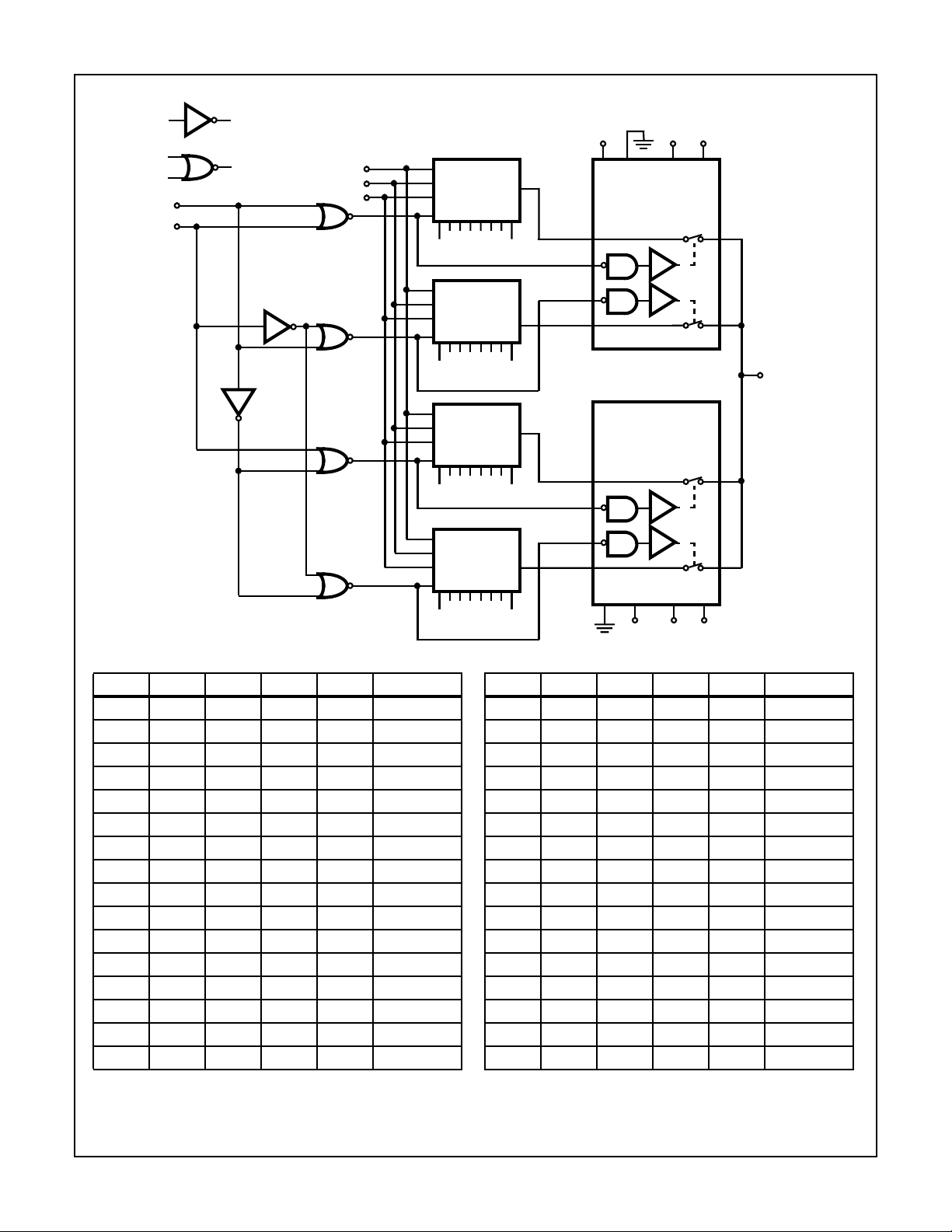
FIGURE 8. 1 OF 16 CHANNEL MULTIPLEXER USING TWO IH6108s. O VER V OL TAGE PR OTECTION IS MAINTAINED BETWEEN ALL
CHANNELS, AS IS BREAK-BEFORE-MAKE SWITCHING.
12-133
Page 7
IH6108
TTL/CMOS INVERTER
TTL/CMOS NOR GATE
A
3
A
4
TRUTH TABLE
+5V
A
0
A
1
A
2
IH6108
1 OUT OF 8
EN
A
A
A
EN
A
A
A
EN
A
A
A
EN
MUX
1
ANALOG INPUTS
0
IH6108
1
1 OUT OF 8
2
MUX
9
ANALOG INPUTS
0
IH6108
1
1 OUT OF 8
2
MUX
17
ANALOG INPUTS
0
IH6108
1
1 OUT OF 8
2
MUX
25
ANALOG INPUTS
8
16
24
32
VL GND V- V+
S
1
IN
1
IN
2
S
2
S
3
IN
3
IN
4
S
4
GND
-15V
IH5053
IH5053
LV V-V+
+15V+5V
+15V
S
1
S
2
S
3
S
4
-15V
D
1
D
2
V
OUT
D
3
D
4
TRUTH TABLE
A
A
4
A
3
A
2
A
1
0
ON SWITCH
00000 S1
00001 S2
00010 S3
00011 S4
00100 S5
00101 S6
00110 S7
00111 S8
01000 S9
01001 S10
01010 S11
01011 S12
01100 S13
01101 S14
01110 S15
01111 S16
NOTE: TTL inverter must have pullup resistor to +5V to drive EN input.
FIGURE 9. 1 OF 32 CHANNEL MULTIPLEXER USING FOUR IH6108s, AND TWO IH5053s AS A SUBMULTIPLEXER
A
4
A
3
A
2
A
1
A
0
ON SWITCH
10000 S17
10001 S18
10010 S19
10011 S20
10100 S21
10101 S22
10110 S23
10111 S24
11000 S25
11001 S26
11010 S27
11011 S28
11100 S29
11101 S30
11110 S31
11111 S32
12-134
Page 8
Schematic Diagram
IH6108
1) A0’ OR A0’
’ OR A1’
2) A
1
’ OR A2’
3) A
2
1
2
3
ADDRESS
DECODER
S
1
S
2
S
3
S
4
S
5
S
6
S
7
P
V-V-
A
X
S
8
ADDRESS
INPUT
EN
V-
N
LEVEL
SHIFTER
GND V-
D
AX’
AX’
EN
EN
V+
V-
GND
INPUT BUFFER
AND
LEVEL SHIFTER
GND V-
V++
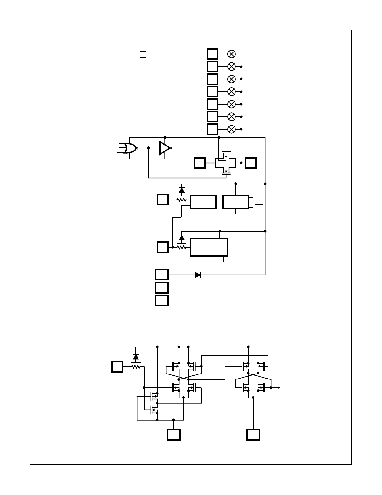
FIGURE 10. IH6108 SCHEMATIC DIAGRAM
V++
P
N
P
N
P
N
P
N
P
N
EN’
GND
FIGURE 11. ENABLE INPUT AND LEVEL SHIFTER
12-135
V-
Page 9
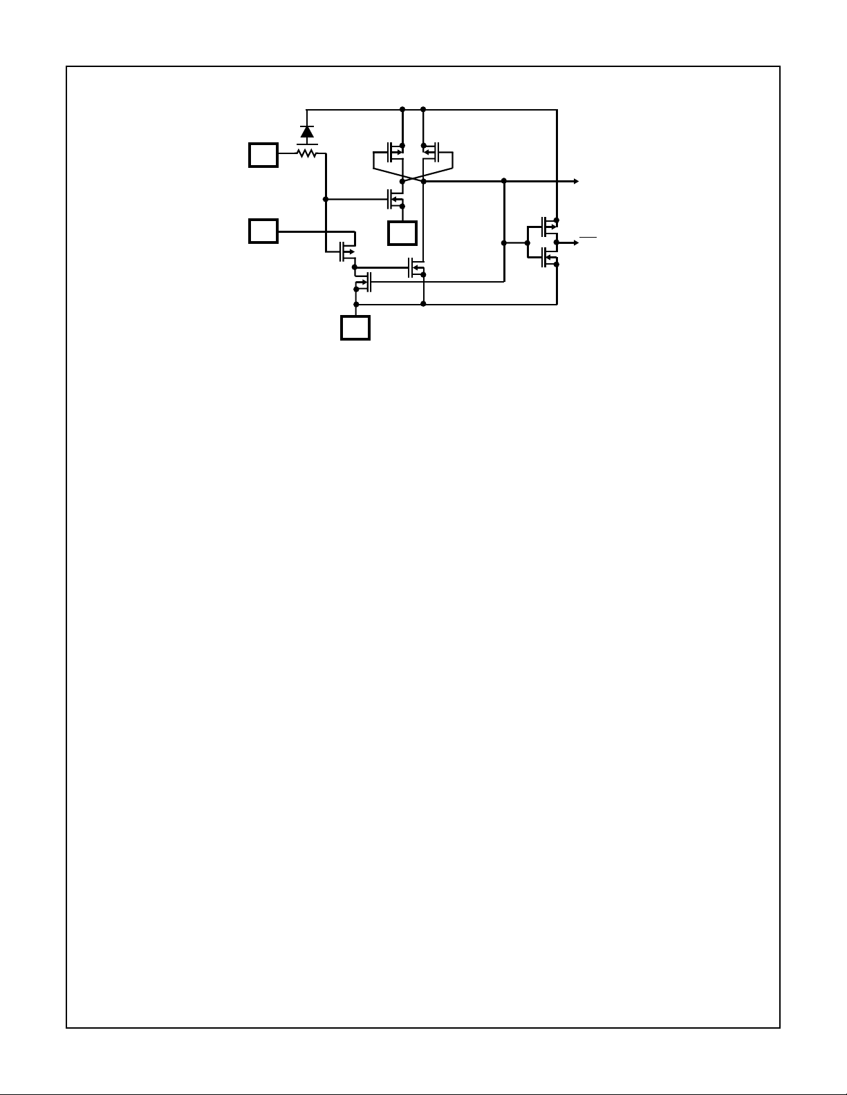
IH6108
V++
P
N
A
EN
P
X
N
GND
V++
P
N
V-
FIGURE 12. ADDRESS INPUT AND LEVEL SHIFTER
AX’
P
A
’
X
N
12-136
 Loading...