

Page 1
IH5352
Data Sheet July 1999
Quad SPST, CMOS RF/Video Switch
The IH5352 is a quad SPST, CMOS monolithic switchwhich
uses a “Series/Shunt” (“T” switch) configuration to obtain
high OFF isolation while maintaining good frequency
response in the ON condition.
Construction of remote and portable video equipment with
extended battery life is facilitated by the extremely low
current requirements. Switching speeds are typically
t
= 150ns and t
ON
= 80ns. “Break-Before-Make”
OFF
switching is guaranteed.
Switch ON resistance is typically 40Ω -50Ωwith±15V power
supplies, increasing to typically 175Ω for ±5V supplies.
Ordering Information
TEMP.
PART NUMBER
RANGE (oC) PACKAGE
IH5352CPE 0 to 70 16 Ld PDIP E16.3
IH5352CBP 0 to 70 20 Ld SOIC M20.3
PKG.
NO.
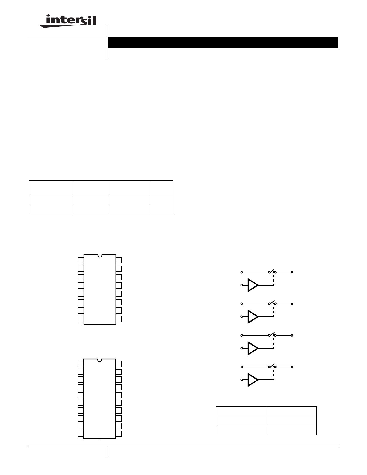
Pinouts
IH5352
(PDIP)
TOP VIEW
16
1
I
IN1
2
S
1
3
I
IN2
4
S
2
5
I
IN3
6
S
3
7
I
IN4
8
S
4
D
1
15
V+
14
D
2
13
GND
D
12
3
11
V-
10
D
4
9
V
L
File Number
3134.2
Features
•r
DS(ON)
• Switch Attenuation Varies Less Than 3dB From DC to
100MHz
• OFF Isolation at 10MHz . . . . . . . . . . . . . . . . . . . . . >70dB
• Crosstalk Isolation at 10MHz . . . . . . . . . . . . . . . . . >60dB
• Compatible With TTL, CMOS Logic
• Wide Operating Power Supply Range
• Power Supply Current . . . . . . . . . . . . . . . . . . . . . . . <1µA
• “Break-Before-Make” Switching
• Fast Switching (Typ). . . . . . . . . . . . . . . . . . . . 80ns/150ns
. . . . . . . . . . . . . . . . . . . . . . . . . . . . . . . . . . . 75Ω
Applications
• Video Switch
• Communications Equipment
• Disk Drives
• Instrumentation
•CATV
Functional Diagram
SWITCH STATE SHOWN FOR LOGIC “0” INPUT
S
1
I
IN1
S
2
I
IN2
D
1
D
2
I
NC
I
I
NC
I
IN1
S
IN2
S
IN3
S
IN4
S
1
2
3
4
1
2
3
4
5
6
7
8
9
10
IH5352
(SOIC)
TOP VIEW
1
S
3
I
IN3
D
20
1
V+
19
NC
18
D
17
2
GND
16
D
15
3
V-
14
NC
13
12
D
4
11
V
L
CAUTION: These devices are sensitive to electrostatic discharge; follow proper IC Handling Procedures.
http://www.intersil.com or 407-727-9207 | Copyright © Intersil Corporation 1999
S
4
I
IN4
TRUTH TABLE
LOGIC SWITCHES
0 Off
1On
D
3
D
4
Page 2
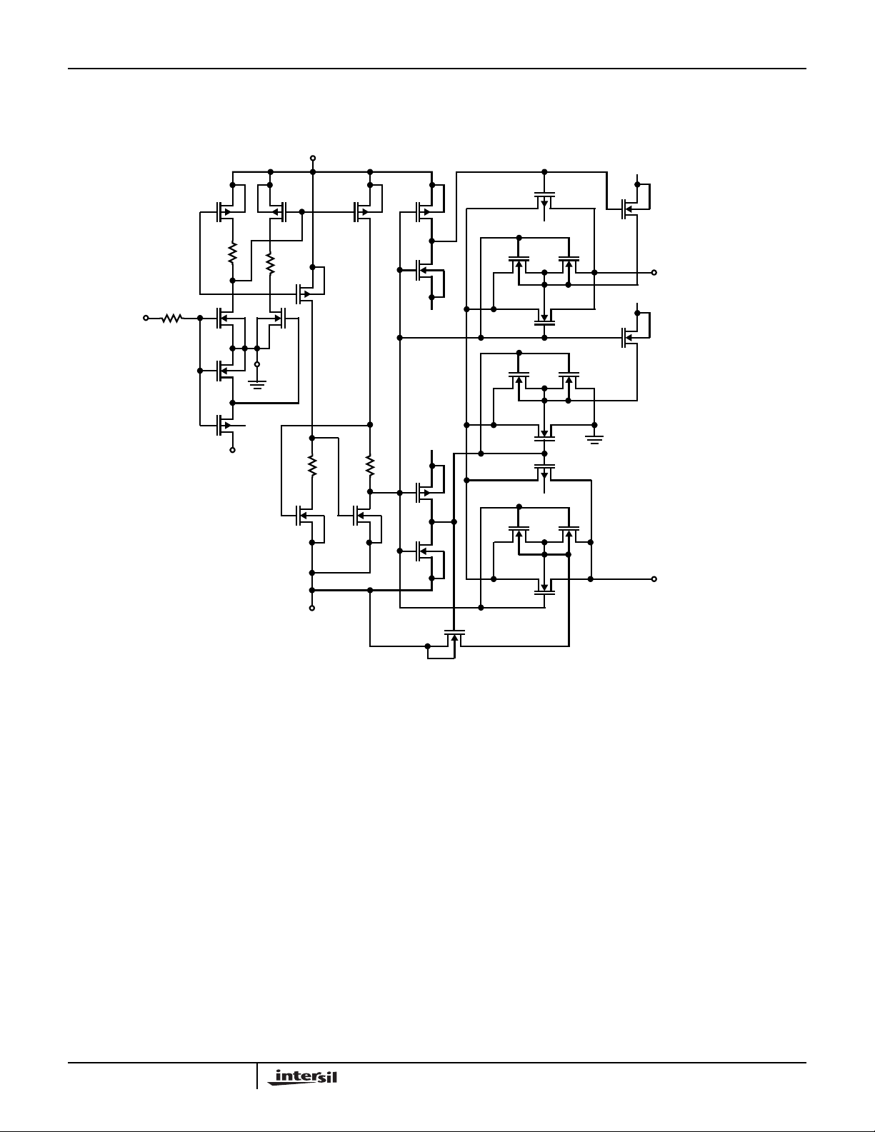
Schematic Diagram
Q
3
10kΩ
Q
TTL
1
Q
5kΩ
Q
IH5352
1
/4 IH5352
+15V
-15V
Q
7
5
Q
20
Q
18
+15V
Q
19
3
Q
8
-15V
Q
16
Q
17
S
-15V
Q
22
Q
9
Q
10
5
+15V
Q
+15V
21
Q
15
+5V
+15V
3kΩ5kΩ
Q
12
Q
4
Q
6
Q
11
D
Q
-15V
Q
14
13
2
Page 3
IH5352
Absolute Maximum Ratings Thermal Information
V+ to Ground . . . . . . . . . . . . . . . . . . . . . . . . . . . . . . . . . . . . . . +18V
V- to Ground. . . . . . . . . . . . . . . . . . . . . . . . . . . . . . . . . . . . . . . .-18V
VL to Ground . . . . . . . . . . . . . . . . . . . . . . . . . . . . . . . . . . . . V+ to V-
Logic Control Voltage. . . . . . . . . . . . . . . . . . . . . . . . . . . . . . V+ to V-
Analog Input Voltage . . . . . . . . . . . . . . . . . . . . . . . . . . . . . . V+ to V-
Current (Any Terminal). . . . . . . . . . . . . . . . . . . . . . . . . . . . . . . 50mA
Operating Conditions
Temperature Range . . . . . . . . . . . . . . . . . . . . . . . . . . . 0oC to 70oC
Supply Voltage Range
V+, VL. . . . . . . . . . . . . . . . . . . . . . . . . . . . . . . . . . . . . . 5V to 15V
V- . . . . . . . . . . . . . . . . . . . . . . . . . . . . . . . . . . . . . . . . -5V to -15V
CAUTION: Stresses above those listed in “Absolute Maximum Ratings” may cause permanent damage to the device. This is a stress only rating and operationofthe
device at these or any other conditions above those indicated in the operational sections of this specification is not implied.
NOTE:
1. θJA is measured with the component mounted on an evaluation PC board in free air.
Thermal Resistance (Typical, Note 1) θJA (oC/W)
SOIC Package . . . . . . . . . . . . . . . . . . . . . . . . . . . . . 90
PDIP Package . . . . . . . . . . . . . . . . . . . . . . . . . . . . . 90
Maximum Junction Temperature (Plastic Packages) . . . . . . .150oC
Maximum Storage Temperature Range. . . . . . . . . . -65oC to 150oC
Maximum Lead Temperature (Soldering, 10s). . . . . . . . . . . . 300oC
(SOIC - Lead Tips Only)
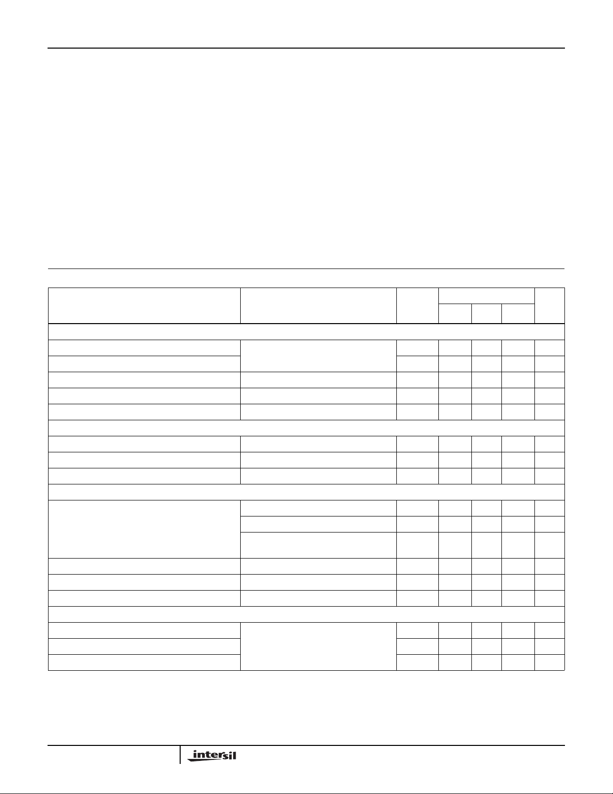
Electrical Specifications V+ = +15V, V
= +5V, V- = -15V, Unless Otherwise Specified
L
(NOTE 2)
(NOTE 4)
TYP
PARAMETER TEST CONDITIONS
25oC
UNITS0oC25oC70oC
DYNAMIC CHARACTERISTICS
Turn ON Time, t
Turn OFF Time, t
ON
OFF
Figure 1 150 - - - ns
80 - - - ns
OFF Isolation, OIRR Figure 2 70 - - - dB
Crosstalk, CCRR Figure 3 -60 - - - dB
Switch Attenuation 3dB Frequency, f
3dB
Figure 4 100 - - - MHz
DIGITAL INPUT CHARACTERISTICS
Logic “1” Input Voltage, V
Logic “0” Input Voltage, V
Input Logic Current, I
IN
IH
IL
VIN > 2.4V or < 0V 0.1 ±1 ±110µA
>2.4 - - - V
<0.8 - - - V
ANALOG SWITCH CHARACTERISTICS
Drain-Source ON Resistance, r
DS(ON)
VD = ±5V, IS = 10mA, VIN≥ 2.4V 50 75 75 100 Ω
VD = ±10V, IS = 10mA, VIN≥ 2.4V 100 150 150 175 Ω
V+ = VL = +5V, VIN = 3V, V- = -5V,
175 300 300 350 Ω
VD= ±3V, IS = 10mA
On Resistance Match Between Channels, ∆r
Switch OFF Leakage Current, I
Switch ON Leakage Current, I
D(OFF)
D(ON)
+ I
or I
S(ON)
DS(ON)IS
S(OFF)
= 10mA, VD = ±5V 5 ---Ω
V
= ±5V or ±14V, VIN≤ 0.8V (Note 3) - - ±2 100 nA
S/D
V
= ±5V or ±14V, VIN≥ 2.4V - - ±2 100 nA
S/D
POWER SUPPLY CHARACTERISTICS
Positive Supply Quiescent Current, I+ VIN = 0V or +5V 0.1 1 1 10 µA
Negative Supply Quiescent Current, I- 0.1 1 1 10 µA
Logic Supply Quiescent Current, I
L
0.1 1 1 10 µA
NOTES:
2. Typical values are not tested in production. They are given as a design aid only.
3. Positive and negative voltages applied to opposite sides of switch, in both directions successively.
4. Min or Max value, unless otherwise specified.
3
Page 4
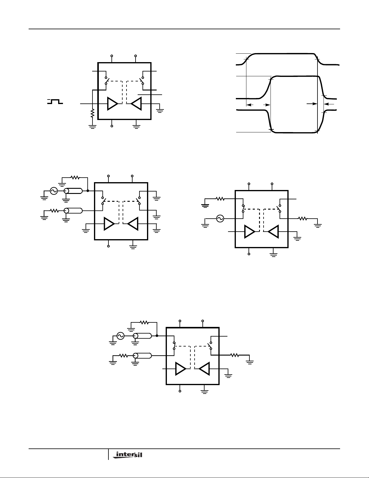
Test Circuits and Waveforms
15V
S
V+ V
1
D
1
IN
1
-15V
+3V
0V
V
ANALOG
TTL IN
RL = 100Ω
(±5V)
V
OUT
NOTE: Only one channel shown. Others act identically.
FIGURE 1A. TEST CIRCUIT
5V
L
GND
S
2
D
2
IN
2
IH5352
FIGURE 1. t
ON
(V
ANALOG
(V
ANALOG
AND t
OFF
+3V
TTL
INPUT
≈ +3.5V
V
OUT
+ 5V)
V
OUT
- 5V)
≈ -3.5V
0V
0V
0V
50%
90%
t
ON
10%
FIGURE 1B. MEASUREMENT POINTS
t
50%
10%
OFF
90%
V
IN
V
OUT
75Ω
V
OIRR 20Log
IN
5V 10V
()at f± 10MHz==
=
75Ω
RG-59
COAX
RG-59
COAX
P-P
V
IN
--------------- -
V
OUT
15V
V+ V
S
1
D
1
IN
1
V-
-15V
5V
L
GND
S
2
D
2
IN
2
NOTE: Only one channel shown. Others act identically.
FIGURE 2. OFF ISOLATION TEST CIRCUIT
75Ω
V
IN
RG-59
COAX
V
OUT
75Ω
RG-59
COAX
+5V
15V
V+ V
S
1
D
1
IN
1
75Ω
V
IN
+5V
V
225mV
IN
CCRR 20Log
RMS
=
FIGURE 3. CROSSTALK TEST CIRCUIT
5V
S
L
2
D
2
IN
2
15V
V+ V
S
1
D
1
IN
1
V-
-15V
atf 10MHz==
V
OUT
--------------- -
V
IN
NC
75Ω
5V
L
GND
S
2
OPEN
75Ω
D
2
V
OUT
IN
2
V-
-15V
ATTN: 20Log
=
GND
R
L
------------------------------------
r
+
DS ON()RL
Nominally, at DC, ATTN equals -4dB. When the attenuation reaches -1dB, the frequency at which this occurs is f
NOTE: Only one channel shown. Others act identically.
FIGURE 4. SWITCH ATTENUATION TEST CIRCUIT
4
3dB
.
Page 5
Detailed Description
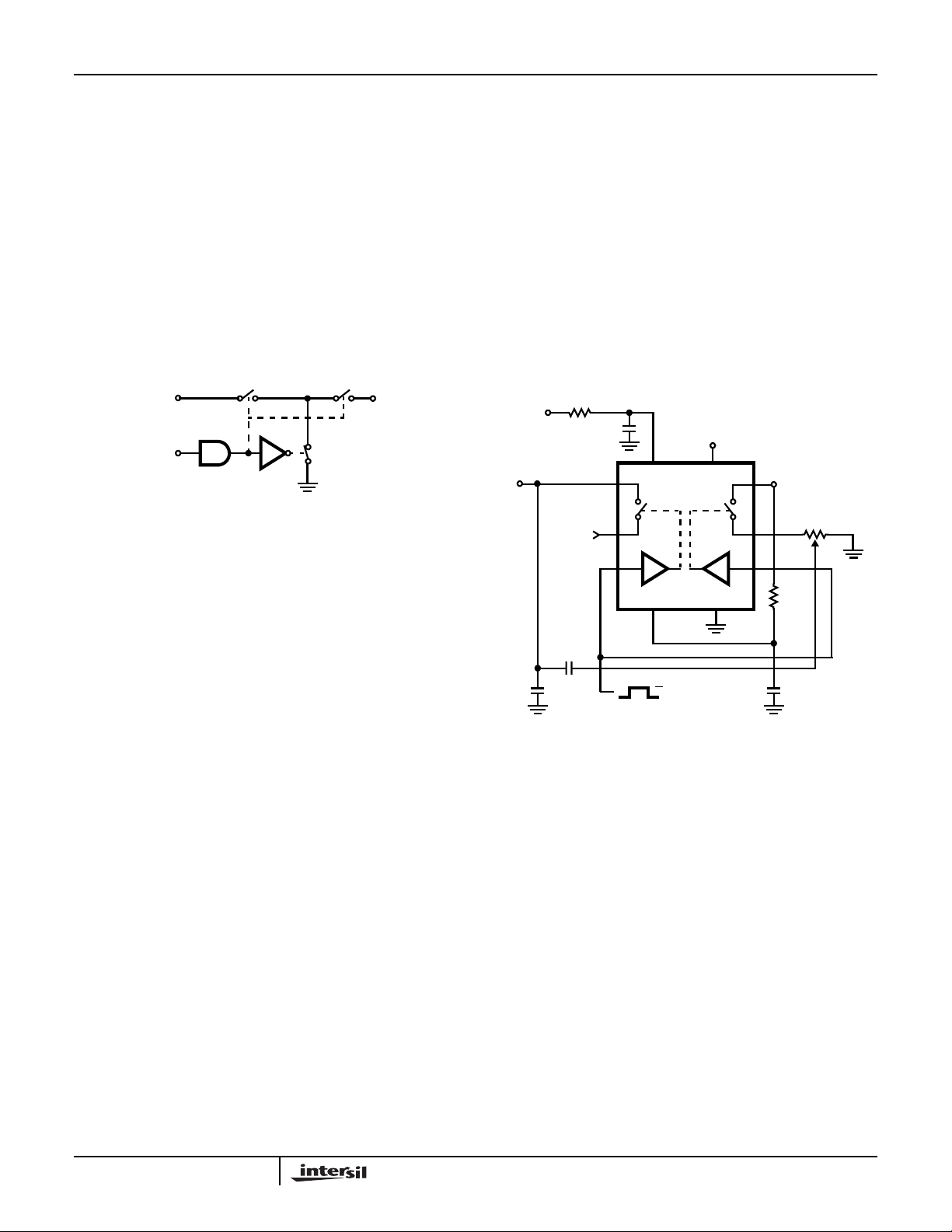
Figure 5 shows the internal circuit of one channel of the
IH5352. Here, a shunt switch is closed, and the two series
switches are open when the video switch channel is open or
off. This provides much better isolation between the input
and output terminals than a simple series switch does,
especially at high frequencies. The result is excellent offisolation in the Video and RF frequency ranges when
compared to conventional analog switches.
The control input level shifting circuitry is very similar to that
of the IH5140 series of Analog Switches, and gives very high
speed, guaranteed “Break-Before-Make” action, low static
power consumption and TTL compatibility.
IH5352
Since individual parts are very consistent in their charge
injection, it is possible to replace the potentiometer with a
pair of fixed resistors, and achieve less than 5mV error for
all devices without adjustment.
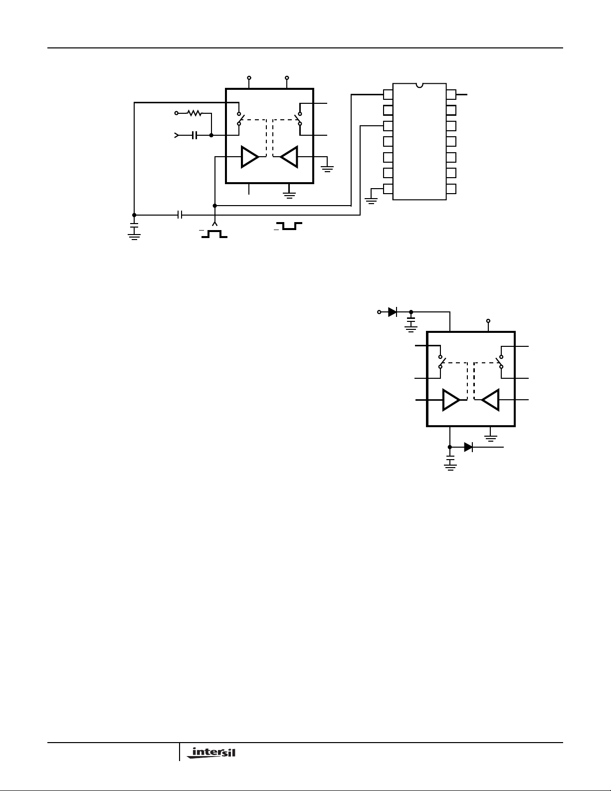
An alternative arrangement, using a standard TTL inverter to
generate the required inversion, is sho wn in Figure 7. The
capacitor needs to be increased, and becomes the only method
of adjustment. A fixed value of 22pF is good for analog values
referred to ground, while 35pF is optimum f or AC coupled
signals referred to -5V as shown in the figure. The choice of -5V
is based on the virtual disappearance at this analog level of the
transient component of switching charge injection. This
combination will lead to a virtually “glitch-free” switch.
SWITCH
SOURCE
(VIDEO INPUT)
LOGIC
CONTROL
INPUT
SHUNT
SWITCH
DRIVER
TRANSLATOR
SWITCH
DRAIN
(VIDEO
OUTPUT)
NOTE: 1 channel of 4 shown.
FIGURE 5. INTERNAL SWITCH CONFIGURATION
Typical Applications
Charge Compensation Techniques
Charge injection results from the signals out of the level
translation circuit being coupled through the gate-channel
and gate-source/drain capacitances to the switch inputs and
outputs. This feedthrough is particularly troublesome in
Sample-and-Hold or Track-and-Hold applications, as it
causes a Sample (Track) to Hold offset. The IH5352 has a
typical injected charge of 30pC-50pC (corresponding to
30mV-50mV on a 1000pF capacitor), at V
This Sample (Track) to Hold offset can be compensated by
bringing in a signal equal in magnitude but of the opposite
polarity. The circuit of Figure 6 accomplishes this charge
injection compensation by using one side of the device as a
S & H (T & H) switch, and the other side as a generator of a
compensating signal. The 1kΩ potentiometer allows the user
to adjust the net injected charge to exactly zero for any
analog voltage in the -5V to +5V range.
of about 0V.
S-D
OUT
75Ω
ANALOG
INPUT
10pF
C
HOLD
1000pF
1µF
V+ V
S
1
D
1
IN
1
V-
+3V
TTL IN (STROBE)
0V
step at V
P-P
5V
S
L
2
D
2
IN
2
GND
with no analog (AC)
OUT
15V
V
NOTE: Adjust pot for 0mV
signal present.
FIGURE 6. CHARGE INJECTION COMPENSATION
-15V
1kΩ CERMET
NOT WIRE
WOUND (NOTE)
75Ω
1µF
5
Page 6
IH5352
15V
DC BIAS
VOLTAGE
= -5V
ANALOG
INPUT
22pF-35pF
C
HOLD
1000pF
V
OUT
75Ω
1µF
+3V
0V
TTL CONTROL IN
V+ V
S
1
D
1
IN
1
V-
-15V
+4V
≈
0V
FIGURE 7. ALTERNATIVE COMPENSATION CIRCUIT
Overvoltage Protection
If sustained operation with no supplies but with analog
signals applied is possible, it is recommended that diodes
(such as 1N914) be inserted in series with the supply lines to
the IH5352. Such conditions can occur if these signals come
from a separate power supply or another location, for
example. The diodes will be reverse biased under this type
of operation, preventing heavy currents from flowing from the
analog source through the IH5352.
The same method of protection will provide over ±25V
overvoltage protection on the analog inputs when the
supplies are present. The schematic for this connection is
shown in Figure 8.
5V
L
GND
+5V
14
13
12
11
10
9
8
V+ V
V-
1N914
1µF
5V
L
GND
IN
S
D
-15V
2
2
2
15V
1
2
3
4
5
6
7
1N914
SN7400
1µF
S
1
D
1
IN
1
S
2
D
2
IN
2
FIGURE 8. OVERVOLTAGE PROTECTION
6
Page 7
Typical Performance Curves
IH5352
70
PIN 3 = +15V, PIN 7 = -15V
PIN 10 = +5V, T
60
(Ω)
50
DS(ON)
r
40
30
-15
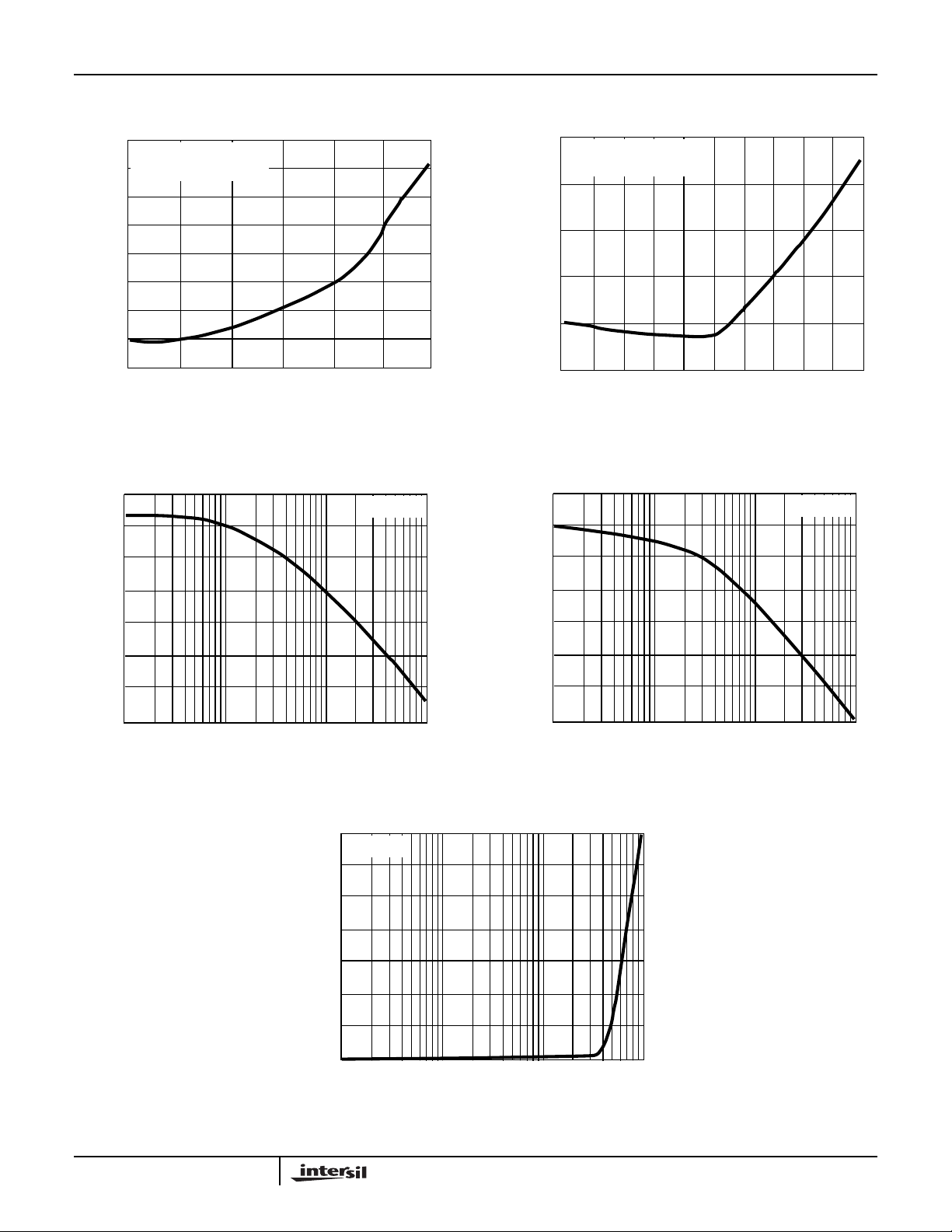
FIGURE 9. r
DS(ON)
POWER SUPPLIES
100
90
80
= 25oC
A
-10 -5 10 1505
ANALOG INPUT VOLTAGE (V)
vs ANALOG INPUT VOLTAGE WITH ±15V
TA = 25oC
180
PIN 3 = PIN10 = +5V
PIN 7 = -5V, T
160
140
(Ω)
DS(ON)
120
r
100
80
-5 50
FIGURE 10. r
DS(ON)
POWER SUPPLIES
-100
-90
-80
= 25oC
A
ANALOG INPUT VOLTAGE (V)
vs ANALOG INPUT LEVEL WITH ±5V
TA = 25oC
70
60
50
OFF ISOLATION (dB)
40
30
FREQUENCY (MHz)
1001010.1
-70
-60
CROSSTALK (dB)
-50
-40
-30
1001010.1
FREQUENCY (MHz)
FIGURE 11. OFF ISOLATION vs FREQUENCY (SEE FIGURE 2) FIGURE 12. CROSSTALK vs FREQUENCY (SEE FIGURE 3)
-3.3
TA = 25oC
-3.4
-3.5
-3.6
-3.7
-3.8
SWITCH ATTENUATION (dB)
-3.9
-4.0
FREQUENCY (MHz)
1001010.1
FIGURE 13. SWITCH ATTENUATION vs FREQUENCY (RL=75Ω, SEE FIGURE 4)
7
Page 8
Die Characteristics
IH5352
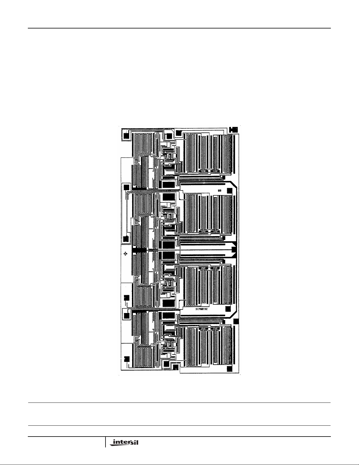
DIE DIMENSIONS:
2617µm x 5233µm
METALLIZATION:
Type: Al
Thickness: 10k
Å ±1kÅ
Metallization Mask Layout
PASSIVATION:
Type: PSG/Nitride
PSG Thickness: 7k
Å ±1.4kÅ
Nitride Thickness: 8kÅ ±1.2kÅ
WORST CASE CURRENT DENSITY:
4
2
9.1 x 10
IH5352
S
1
IN
2
IN1D
1
A/cm
V+
(SUBSTRATE)
D
2
S
2
GND
IN
3
D
3
S
3
IN
4
S
V
4
L
V-
D
4
All Intersil semiconductor products are manufactured, assembled and tested under ISO9000 quality systems certification.
Intersil semiconductor products are sold by description only .Intersil Corporation reserves the right to make changes in circuit design and/or specifications at any time without notice. Accordingly, the reader is cautioned to verify that data sheets are current before placing orders. Information furnished by Intersil is believed to be accurate and
reliable. However, no responsibility is assumed by Intersil or its subsidiaries for its use; nor for any infringements of patents or other rights of third parties which may result
from its use. No license is granted by implication or otherwise under any patent or patent rights of Intersil or its subsidiaries.
For information regarding Intersil Corporation and its products, see web site http://www.intersil.com
8
 Loading...