

Page 1
Silicon Bipolar MMIC
3.5 and 5.5 GHz Divide-by-4
Static Prescalers
Technical Data
IFD-53010
IFD-53110
Features
• Wide Operating Frequency
Range:
IFD-53010: 0.15 to 5.5 GHz
IFD-53110: 0.15 to 3.5 GHz
• Low Phase Noise:
-143 dBc/Hz @ 1 kHz Offset
• Output Power: -5 dBm Typ.
• Single Supply Voltage
Vcc = 5 V or Vee = -5 V
• On-Chip Terminations
Provide Good Input and
Output VSWRs
• Hermetic Gold-Ceramic
Surface Mount Package
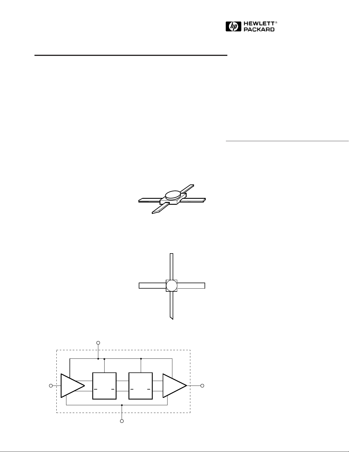
Functional Block Diagram
1
V
CC
RF INPUT
4
CQ CQ
CQ CQ
3
100 mil Stripline Package Description
Hewlett-Packard's IFD-53010 and
IFD-53110 are low phase noise
silicon bipolar static digital
frequency dividers using two
scaled Emitter-Coupled-Logic
(ECL) master-slave D flip-flops
and buffer amplifiers. They are
housed in hermetic high reliability
surface mount packages suitable
Pin Configuration
V
3
EE
4
RF INPUT RF OUTPUT
V
1
CC
V
EE
2
RF OUTPUT
2
for commercial, industrial, and
military applications. Typical
applications include stabilized or
digitally controlled local oscillators for GPS, SATCOM or
military receivers, and frequency
synthesizers and counters in
instrumentation systems. The
IFD-53110 is a lower cost selected
version of the IFD-53010, and is
distinguished by a reduced
operating frequency range.
The IFD series of frequency
dividers is fabricated using
Hewlett-Packard's 18 GHz, ft,
ISOSAT™-2 silicon bipolar
process which uses nitride selfalignment, submicrometer
lithography, trench isolation, ionimplantation, gold metallization
and polyimide intermetal
dielectric and scratch protection
to achieve excellent device
uniformity, performance, and
reliability.
7-151
5965-9115E
Page 2
Absolute Maximum Ratings
Symbol Parameter Units Absolute Maximum
[1]
Vcc - V
P
diss
P
in
T
j
T
STG
Thermal Resistance
Notes:
1, Operation of this device above any one of these parameters may cause permanent damage.
2. T
= 25°C.
case
3. Derate at 9.3 mW/°C for TC ≥ 130°C.
Device Voltage V 8
ee
Power Dissipation
[2,3]
m W 650
RF Input Power dBm +15
Junction Temperature °C 200
Storage Temperature °C -65 to +200
[2]
: θjc = 107° C/W
Guaranteed Electrical Specifications, IFD-53010 and IFD-53110
T
= 25° C, ZO = 50 Ω, V
A
Symbol Parameters and Test Conditions Units Min. Typ. Max.
IFD-53010:
F
MAX
Maximum Clock Frequency Pin = -10 dBm (200 mVpp) GHz 5.5 6.0
IFD-53110:
F
MAX
I
CC
Maximum Clock Frequency Pin = -10 dBm (200 mVpp) GHz 3.5 5.0
IFD-53010 and IFD-53110: Supply Current mA 35 43 50
- Vee = 5.0 V
cc
Typical Design Information, T
All values apply to both IFD-53010 and IFD-53110. f
= 25° C, Z0 = 50 Ω, V
A
is 5 GHz for IFD-53010 and 3 GHz for IFD-53110 (unless
test
- Vee = 5.0 V, Pin = -10 dBm.
cc
otherwise noted).
Symbol Parameters and Test Conditions Units Value
F
MIN
P
Minimum Clock Frequency
in
Input Sensitivity f = f
[1]
test
MHz 150
dBm -22
mVpp 50
P
out
Output Power f = 0.15 to f
test
dBm -5
mVpp 355
VSWR Input VSWR f = 0.15 to f
Output VSWR f = 0.15 to f
test
test
2.0:1
2.5:1
PN SSB Phase Noise f = 3 GHz, 1 kHz offset dBc/Hz -143
f = 5 GHz, 1 kHz offset (IFD-53010 only) -138
T
r
T
f
Note:
1. Minimum clock frequency when driven from a sinusoidal input. Operation to lower frequencies is possible when using input signals
with faster rise times, such as occurs in the case of a cascade of two or more IFDs.
Output Rise Time, 20% - 80% f = f
Output Fall Time, 20% - 80% f = f
test
test
psec 145
psec 85
7-152
Page 3

Typical Performance, T
= 25° C, ZO = 50 Ω, V
A
- Vee = 5.0 V
cc
Graphs apply to both IFD-53010 and IFD-53110 (unless otherwise noted).
0
IFD-53010 &
-10
-20
-30
-40
INPUT SENSITIVITY (dBm)
-50
IFD-53110
IFD-53010
0 1 23 45 67
FREQUENCY (GHz)
Figure 1. Input Sensitivity vs. Input
Frequency and Recommended
Operating Ranges for Nominal
Operating Conditions (T = 25°C , V
Vee = 5 V).
70
60
50
40
CC
I (mA)
30
20
10
+ 125°C
+ 25°C
- 55°C
0
IFD-53010 &
IFD-53110
-10
-20
-30
-40
INPUT SENSITIVITY (dBm)
-50
01 2345 67
FREQUENCY (GHz)
Figure 2. Input Sensitivity vs. Input
Frequency and Recommended
Operating Ranges for Worst Case
-
Operating Conditions (-55° C < T <
cc
125° C and 4.5 V < V
3:1
OUTPUT
2:1
VSWR
INPUT
IFD-53010
- Vee < 5.5 V.
cc
0
-10
-20
-30
-40
INPUT SENSITIVITY (dBm)
-50
01 234567
-55°C
25°C
125°C
FREQUENCY (GHz)
Figure 3. Input Sensitivity vs. Input
Frequency and Temperature
(Vcc - Vee = 5 V).
2
0
5.5 V
-2
5.0 V
-4
4.5 V
OUTPUT LEVEL (dBm)
-6
0
1234560
V-V
(V)
CC
EE
Figure 4. Device Current vs. Voltage
and Temperature.
-
60
-
80
-100
-120
SSB PHASE NOISE (dBc/Hz)
-140
2 TO 4 GHz
(IFD-53010 & IFD-53110)
-160
1 1kHz 1MHz
5 GHz (IFD-53010)
OFFSET FREQUENCY
Frequency, and Input Frequency.
1:1
10 100 1000 10000
FREQUENCY (MHz)
Figure 5. Input and Output VSWR vs.
Frequency.
+100
V
in
0
in
V (mV)
V
out
-100
200
Figure 8. IFD-53010 Typical Output Response with 5 GHz Input.Figure 7. SSB Phase Noise vs. Offset
7-153
-8
10 100 1000 10000
FREQUENCY (MHz)
Figure 6. Output Power Level vs. Input
Frequency and Vcc - Vee.
TIME (psec)
+200
0
-200
out
V (mV)
Page 4

BLOCKING CAPACITORS ARE 1000 pF TYP.
BYPASS CAPACITORS ARE 47 nF min.
BLOCKING CAPACITORS MAY BE OMITTED
IF GENERATOR AND LOAD ARE AT V LEVEL.
TRANSMISSION LINES ARE 50 .
CC
V = -5.0 V
EE
F
RF INPUT
(50 )
3
C
BL
4
V
CC
PIN:
V = 0 V
CC
C
(47 nF min.)
SWINGS BETWEEN V
1
BY
2
AND V -360 mV
CC
C
BL
RF OUTPUT
CC
F/4
(50 )
Figure 9. Typical ECL Biasing Configuration, IFD-53010 and IFD-53110.
BLOCKING CAPACITORS ARE 1000 pF TYP.
BYPASS CAPACITOR SHOULD BE 47 nF min.
TO ENSURE GOOD SENSITIVITY PERFORMANCE.
TRANSMISSION LINES ARE 50 .
PIN:
V = 0 V
3
EE
C
2
BL
RF OUTPUT
F/4
(50 )
F
RF INPUT
(50 )
C
BL
4
V = 5.0 V
CC
1
C
BY
(47 nF min.)
Figure 10. Typical RF Biasing Configuration, IFD-53010 and IFD-53110.
LO OUTPUT
PROGRAMMABLE
DIVIDER
PHASE DETECTOR
STABLE REFERENCE
VCO
AFC
DIV. BY 4
LPF
Figure 11. Typical Stabilized LO Configuration, IFD-53010 and IFD-53110.
7-154
Page 5

TEST SYSTEM
Z = 50
O
PIN: 3
V = -5.0 V
EE
10 dB
GENERATOR OUTPUT:
FREQUENCY = f
LEVEL = P + 10 dB (INTO 50 LOAD)
in
4
1
V = 0 V
CC
2
10 dB
SPECTRUM
ANALYZER
P
OUT
f/4
Z = 50
in
Figure 12. Sensitivity Test Configuration, IFD-53010 and IFD-53110.
Package Dimensions
100 mil Stripline Package
1.02
(0.040)
4
0.51
(0.20)
13
NOTES: (unless otherwise specified)
1. DIMENSIONS ARE IN mm (INCHES)
2. TOLERANCES: in .xxx = ± .005
mm .xx = ± .13
0.76
(0.030)
0.10 ± 0.05
(0.004 ± 0.002)
2
2.54
(0.100)
12.57 ± 0.76
(0.495 ± 0.030)
O
5
7-155
 Loading...