

Datasheet IDT7MPV6255S66M, IDT7MPV6255S15M, IDT7MPV6253S66M, IDT7MPV6256S66M, IDT7MPV6256S15M Datasheet (Integrated Device Technology)
Page 1
Integrated Device Technology, Inc.
256KB AND 512KB SECONDARY
CACHE MODULES FOR THE
PowerPC
IDT7MPV6253
IDT7MPV6255/56
FEATURES
• For CHRP based PowerPC systems.
• Asynchronous and pipelined burst SRAM options in the
same module pinout
• Low-cost, low-profile card edge module with 178 leads
• Uses Burndy Computerbus connector, part number
ELF182KSC-3Z50
• Operates with external PowerPC CPU speeds up to
66MHz
• Separate 5V (±5%) and 3.3V (+10/-5%) power supplies
• Multiple GND pins and decoupling capacitors for maximum noise immunity
• Presence Detect output pins allow the system to determine the particular cache configuration.
DESCRIPTION
The IDT7MPV6253/55/56 modules belong to a family of
secondary caches intended for use with PowerPC CPUbased systems. The IDT7MPV6253 uses IDT’s 71V256 32K
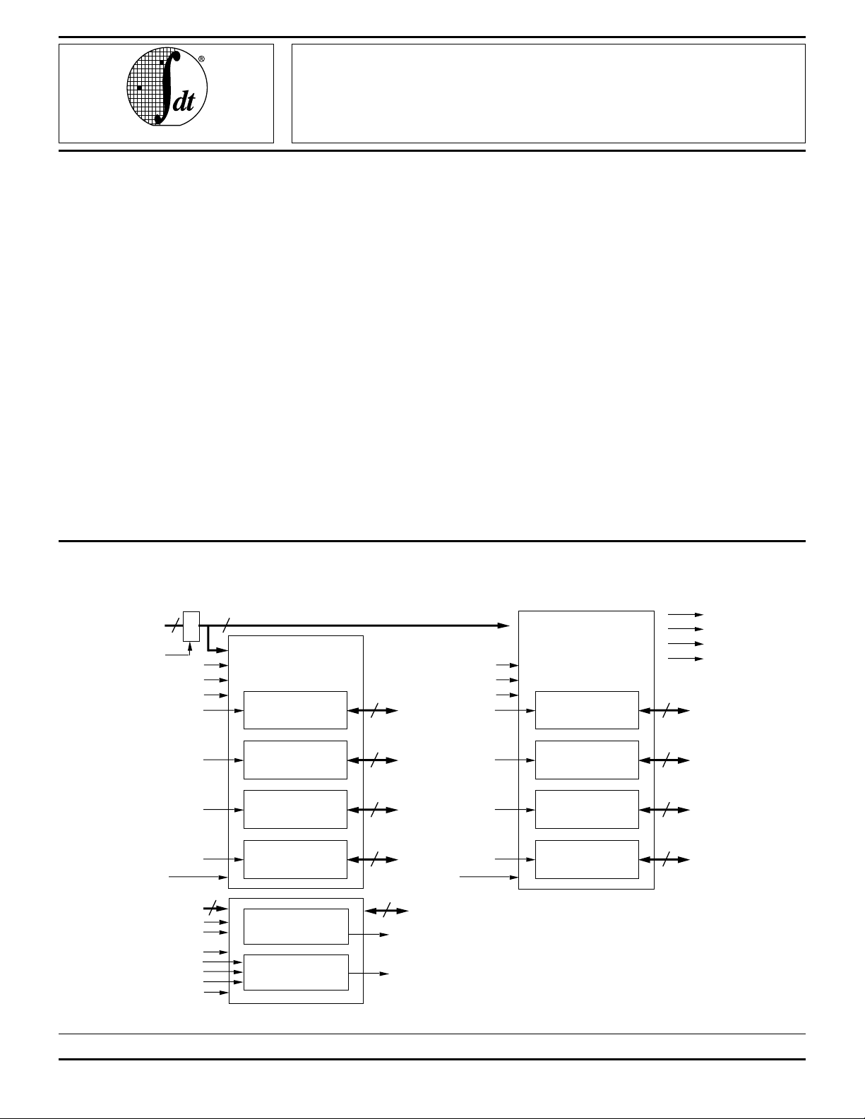
FUNCTIONAL BLOCK DIAGRAM
x 8 asynchronous static RAMs and the IDT7MPV6255/56 use
IDT’s 71V432 32K x 32 pipelined synchronous burst static
RAMs in plastic surface mount packages mounted on a
multilayer epoxy laminate (FR-4) board. In addition, each of
the modules uses the IDT 71216 16K x 15 Cache-Tag static
RAM and IDT FCT logic. Extremely high speeds are achieved
using IDT’s high-reliability, low cost CMOS technology.
The low profile card edge package allows 178 signal leads
to be placed on a package 5.06" long, a maximum of 0.250"
thick and a maximum of 1.08" tall. The module space savings
versus discrete components allows the OEM to design additional functions onto the system or to shrink the size of the
motherboard for reduced cost.
All inputs and outputs are LVTTL-compatible, and operate
from separate 5V (±5%) and 3.3V (+10/-5%) power supplies.
Multiple GND pins and on-board decoupling capacitors ensure maximum protection from noise.
IDT7MPV6253 – 256KB ASYNCHRONOUS VERSION
A14 - A26
STANDBY STANDBY
The IDT logo is a registered trademark of Integrated Device Technology, Inc. PowerPC is a trademark of IBM. Computerbus is trademark of Burndy.
13 13
ALE
ADDRA0
ADDRA1
SRAM OE1
WE#0
WE#1
WE#2
WE#3
A14 - A26
TWE#
TOE#
STANDBY
TCLR#
TVALID
DIRTYIN
CLK
Latch
2
ADDRA0
ADDRA1
32K x 8
Asynchronous
SRAM
32K x 8
Asynchronous
SRAM
32K x 8
Asynchronous
SRAM
32K x 8
Asynchronous
SRAM
13
8K x 12
Tag Field
8K x 2
Status
8
8
8
8
12
TMATCH
DIRTYOUT
DH0 - DH7
DH8 - DH15
DH16 - DH23
DH24 - DH31
2 - A13
A
SRAM OE0
WE#4
WE#5
WE#6
WE#7
32K x 8
Asynchronous
SRAM
32K x 8
Asynchronous
SRAM
32K x 8
Asynchronous
SRAM
32K x 8
Asynchronous
SRAM
8
8
8
8
COMMERCIAL TEMPERATURE RANGE JUNE 1996
1996 Integrated Device Technology, Inc. DSC-3608/2
1
PD0
PD1
PD2
PD3
DL0 - DL7
DL8 - DL15
DL16 - DL23
DL24 - DL31
drw 01
Page 2
IDT7MPV6253/55/56
256KB/512KB CMOS SECONDARY CACHE MODULES FOR THE PowerPC COMMERCIAL TEMPERATURE RANGE
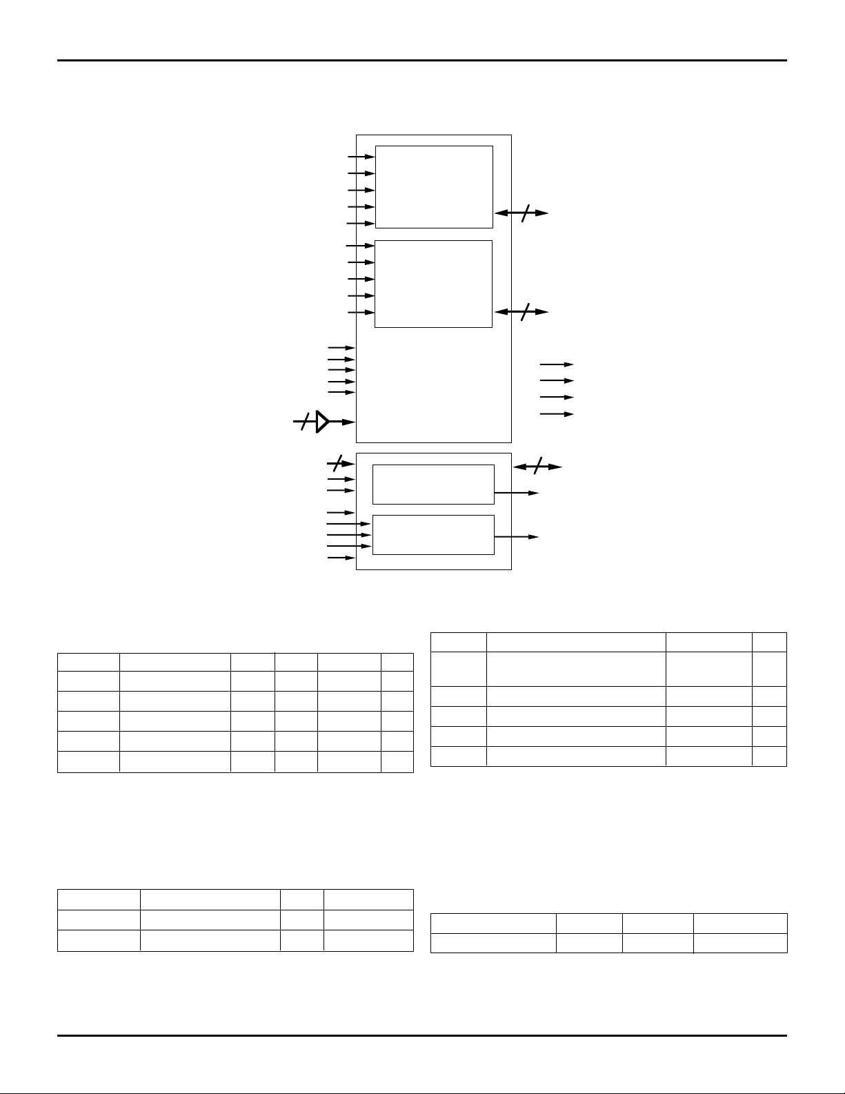
FUNCTIONAL BLOCK DIAGRAM
IDT7MPV6255 – 256KB PIPELINED BURST VERSION
SRAM OE#0
SRAM ADS#0
CNT EN#0
STANDBY
BURST MODE
A14 - A28
15
A14 - A26
TWE#
TOE#
STANDBY
TCLR#
TVALID
DIRTYIN
CLK
WE#0
WE#1
WE#2
WE#3
CLK1
CLK0
WE#4
WE#5
WE#6
WE#7
13
2
32K x 32
Pipelined
Burst
SRAM
32K x 32
Pipelined
Burst
SRAM
8K x 12
Tag Field
8K x 2
Status
32
DH0-31
32
DL0-31
12
PD0
PD1
PD2
PD3
A2 - A13
TMATCH
DIRTYOUT
RECOMMENDED DC
OPERATING CONDITIONS
Symbol Parameter Min. Typ. Max. Unit
VCC3 Supply Voltage 3.14 3.3 3.6 V
VCC5 Supply Voltage 4.75 5.0 5.25 V
GND Supply Voltage 0 0 0.0 V
VIH Input High Voltage 2.2 — VCC + 0.3 V
IL Input Low Voltage –0.5
V
NOTE: tbl 01
1. VIL = –1.0V for pulse width less than 5ns, once per cycle.
(1)
— 0.8 V
RECOMMENDED OPERATING
TEMPERATURE AND SUPPLY VOLTAGE
Power Plane Ambient Temperature GND VCC
VCC3 0°C to +70°C 0V 3.3V +10/-5%
CC5 0°C to +70°C 0V 5.0V ± 5%
V
tbl 02
drw 02
ABSOLUTE MAXIMUM RATINGS
Symbol Rating Value Unit
TERM Terminal Voltage with Respect –0.5 to +4.6 V
V
for VCC3 to GND
TA Operating Temperature 0 to +70 °C
TBIAS Temperature Under Bias –10 to +85 °C
TSTG Storage Temperature –55 to +125 °C
OUT DC Output Current 50 mA
I
NOTE: tbl 03
Stresses greater than those listed under ABSOLUTE MAXIMUM RATINGS
may cause permanent damage to the device. This is a stress rating only and
functional operation of the device at these or any other conditions above those
indicated in the operational sections of this specification is not implied.
Exposure to absolute maximum rating conditions for extended periods may
affect reliability.
SRAM ACCESS TIMES
Module Speed Asych Burst
66MHz 15ns 8.5ns 10ns
NOTE: tbl 04
1. Burst SRAMs are measured by Clock to Data Out (tCD).
(1)
Tag
2
Page 3
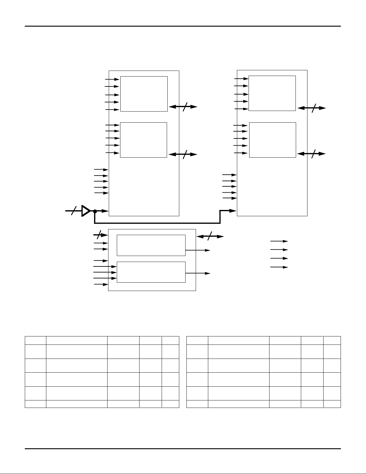
IDT7MPV6253/55/56
256KB/512KB CMOS SECONDARY CACHE MODULES FOR THE PowerPC COMMERCIAL TEMPERATURE RANGE
FUNCTIONAL BLOCK DIAGRAM
IDT7MPV6256 – 512KB PIPELINED BURST VERSION
SRAM OE#0
SRAM ADS#0
BURST MODE
A13 - A28
CNT EN#0
STANDBY
16
A13 - A26
TWE#
TOE#
STANDBY
TCLR#
TVALID
DIRTYIN
CLK
WE#0
WE#1
WE#2
WE#3
CLK1
WE#4
WE#5
WE#6
WE#7
CLK0
14
2
32K x 32
Pipelined
Burst
SRAM
32K x 32
Pipelined
Burst
SRAM
16K x 12
Tag Field
16K x 2
Status
32
DH0-31
32
DL0-31
SRAM OE#1
SRAM ADS#1
CNT EN#1
STANDBY
BURST MODE
12
WE#0
WE#1
WE#2
WE#3
CLK1
WE#4
WE#5
WE#6
WE#7
CLK0
A
1 - A12
TMATCH
DIRTYOUT
32K x 32
Pipelined
Burst
SRAM
32K x 32
Pipelined
Burst
SRAM
32
DH0-31
32
DL0-31
PD0
PD1
PD2
PD3
CAPACITANCE (IDT7MPV6253 )
(1)
(TA = +25°C, f = 1.0 MHz)
Symbol Parameter
C
IN1 Input Capacitance VIN = 0V 15 pF
(Address)
IN2 Input Capacitance VIN = 0V 25 pF
C
(ADDR0-1)
C
IN3 Input Capacitance VIN = 0V 45 pF
(OE#)
IN4 Input Capacitance VIN = 0V 8 pF
C
(WE#, TWE#)
C
I/O I/O Capacitance VOUT = 0V 10 pF
NOTES: tbl 05
1. These parameters are guaranteed by design but not tested.
(1)
Condition Max. Unit
CAPACITANCE (IDT7MPV6255/56 )
(1)
(TA = +25°C, f = 1.0 MHz)
Symbol Parameter
C
IN1 Input Capacitance VIN = 0V 20 pF
(Address)
IN2 Input Capacitance VIN = 0V — pF
C
(ADDR0-1)
C
IN3 Input Capacitance VIN = 0V 15 pF
(OE#)
IN4 Input Capacitance VIN = 0V 8 pF
C
(WE#, TWE#)
C
I/O I/O Capacitance VOUT = 0V 10/20 pF
NOTES: tbl 06
1. These parameters are guaranteed by design but not tested.
3
(1)
Condition Max. Unit
drw 03
Page 4

IDT7MPV6253/55/56
256KB/512KB CMOS SECONDARY CACHE MODULES FOR THE PowerPC COMMERCIAL TEMPERATURE RANGE
PIN CONFIGURATION
90
GND
91
1
PD
92
PD3
93
DH31
94
DH29
95
DH27
96
DH25
97
VCC3
DH23
DH21
DH18
GND
DH
DH14
DH13
VCC5
DH10
DH8
DH6
VCC3
DH4
GND
CLK
GND
DH
DL
DL30
GND
DL
DL27
DL25
VCC5
DL23
DL21
DL19
GND
DL
DL15
DL13
GND
DL
DL8
DL6
VCC3
DL5
DL2
GND
(1)
CLK
GND
(1)
CLK
GND
CC3
V
ADDR1
RSVD
A27
A24
A22
A20
GND
A
A16
A15
A14
VCC3
A10
GND
(2,3)
CC5
V
GND
98
99
100
101
102
103
16
104
105
106
107
108
109
110
111
112
113
114
115
0
116
117
1
118
119
31
120
121
122
29
123
124
125
126
127
128
129
130
131
17
132
133
134
135
136
10
137
138
139
140
141
142
143
144
3
145
146
4
147
148
4
149
150
151
152
153
0
154
155
156
167
158
159
160
18
161
162
163
164
165
166
A8
167
A6
168
169
4
A
170
A2
171
A1
172
173
174
175
176
177
178
SRAM WE3
SRAM WE2
SRAM WE1
SRAM WE0
SRAM WE7
SRAM WE6
SRAM WE5
SRAM WE
(3,4)
SRAM ALE
(3,4)
(2)
SRAM CNT EN
(2,3)
SRAM CNT EN1
BURST MODE
TAG VALID
STANDBY
DIRTYOUT
(1)
TAG WE
(1)
GND
1
PD
2
PD2
3
DH30
4
DH28
5
DH26
6
DH24
7
VCC3
8
DP3
9
DH22
10
DH20
11
DH19
12
GND
13
DH
14
DP2
15
DH15
16
DH12
17
VCC5
18
DH11
19
DH9
20
DP1
21
DH7
22
VCC3
23
DH5
24
DH3
25
DH2
26
DH0
27
DP0
28
GND
29
CLK
30
GND
31
DL
32
DL26
33
DL24
34
DP7
35
VCC5
36
DL22
37
DL20
38
DL18
39
DL16
40
GND
41
DP
42
DL14
43
DL12
44
DL11
45
GND
46
DL
47
DP5
48
DL7
49
DL4
50
VCC3
51
DL3
52
DL1
53
DL0
54
GND
55
CLK
56
GND
57
DP
58
SRAM OE0
59
SRAM OE1
60
VCC3
61
ADDR0
62
RSVD
63
SRAM ADS
64
SRAM ADS1
65
A28
66
A26
67
A25
68
A23
69
GND
70
A
71
A19
72
A17
73
A13
74
VCC3
75
A12
76
A11
77
A9
78
GND
79
A
80
A5
81
A3
82
A0
83
VCC5
84
TAG CLR
85
TAG MATCH
86
TAG OE
87
DIRTYIN
88
GND
89
0
17
28
6
9
4
21
7
(1)
(1)
(1)
(1)
(1)
1
(1)
(1)
(1)
2 (TAG)
(1)
(3,4)
(1)
PIN NAMES
A0 – A28 Address Inputs
ADDR0 - ADDR1 Address Inputs (Asynchronous SRAMs only)
CLK0 - CLK4 Clock Inputs
DH0 - DH31 High Order Cache Data
DL0 - DL31 Low Order Cache Data
PD0 – PD3 Presence Detect Pins
SRAM ADS
SRAM ADS1
SRAM ALE SRAM Address Latch Enable
SRAM CNT EN
SRAM CNT EN1
SRAM OE0 - SRAM Output Enable
SRAM OE1
SRAM WE0 - SRAM Write Enable
SRAM WE1
BURST MODE Burst Mode: 0=Linear, 1=Interleaved
TAG CLR Tag Clear
TAG MATCH Tag Match
TAG VALID Tag Valid
TAG OE Tag Output Enable
TAG WE Tag Write Enable
DIRTYIN Dirty Input Bit
DIRTYOUT Dirty Output Bit
STANDBY Stand By Mode
VCC3 3.3 Volt Power Supply
VCC5 5 Volt Power Supply
GND Ground
NC No Connect
RSVD Reserved
(3)
(2)
0
(2,3)
PRESENCE DETECT TABLE
PD3 PD2 PD1 PD0 Module
NC NC NC NC No cache present
NC GND GND GND IDT7MPV6253
GND GND NC NC IDT7MPV6255
GND NC NC NC IDT7MPV6256
NOTES:
1. These pins are NC (No Connect) on 7MPV6253/55/56.
2. These pins are NC on 7MPV6253.
3. These pins are NC on 7MPV5255.
4. These pins are NC on 7MPV6256.
0 - SRAM Address Strobe
0 - SRAM Control Enable
tbl 07
tbl 08
LOW PROFILE CARD EDGE MODULE
TOP VIEW
drw 04
4
Page 5

IDT7MPV6253/55/56
256KB/512KB CMOS SECONDARY CACHE MODULES FOR THE PowerPC COMMERCIAL TEMPERATURE RANGE
DC ELECTRICAL CHARACTERISTICS
(VCC5 = 5.0V ± 5%, VCC3 = 3.3V ± 10%, TA = 0°C to 70°C)
’53 ’55 ’56
Symbol Parameter Test Condition Min. Max. Max. Max. Unit
|I
LI| Input Leakage Current VCC5 = Max, VIN = GND to VCC —203050µA
(Address) VCC3 = Max
LI| Input Leakage Current VCC5 = Max, VIN = GND to VCC —101020µA
|I
(Data and Control) VCC3 = Max
|ILO| Output Leakage Current VOUT = 0V to VCC3, VCC3 = Max. — 10 10 20 µA
VOL Output Low Voltage IOL = 8mA, VCC3 = Min. — 0.4 0.4 0.4 V
VOH Output HighVoltage IOH= –4mA, VCC3 = Min. 2.4 — — — V
CC3 Operating 3.3V Power VCC3 = Max., STANDBY ≤ VIL, — 1000 500 590 mA
I
Supply Current f = fMAX, Outputs Open
CC5 Operating 5V Power VCC5 = Max., STANDBY ≤ VIL, — 290 290 290 mA
I
Supply Current f = fMAX, Outputs Open
SB3 Standby 3.3V Power VCC3 = Max., STANDBY ≥ VIH, — 100 100 190 mA
I
Supply Current f = fMAX, Outputs Open
I
SB31 Full Standby 3.3V Power VCC3 = Max., STANDBY ≥ VCC3 - 0.2V, f = 0, — 30 30 50 mA
Supply Current V
SB5 Standby 5V Power VCC5 = Max., STANDBY ≥ VIH —303030mA
I
Supply Current f = f
IN ≤ 0.2V or VIN ≥ VCC3 - 0.2V,
Outputs Open
MAX, Outputs Open
tbl 09
AC TEST CONDITIONS – 3.3V POWER SUPPLY
Input Pulse Levels GND to 3.0V
Input Rise/Fall Times 3ns
Input Timing Reference Levels 1.5V
Output Reference Levels 1.5V
Output Load See Figures 1 and 2
tbl 10
+3.3V
320
Ω
DATA
OUT
Ω
350
*including scope and jig capacitances
Figure 1. Output Load
30pF*
+3.3V
320
DATA
OUT
Ω
350
*including scope and jig capacitances
Figure 2. Output Load
OHZ, tCHZ, tOLZ and tCLZ)
(for t
5pF*
Ω
drw 06drw 05
5
Page 6

IDT7MPV6253/55/56
256KB/512KB CMOS SECONDARY CACHE MODULES FOR THE PowerPC COMMERCIAL TEMPERATURE RANGE
PACKAGE DIMENSIONS - IDT7MPV6253
FRONT VIEW
5.050
5.070
1.060
1.080
SIDE VIEW
0.225 MAX
PIN 90
2 X 0.195
IDT7MPV6255
1.060
1.080
0.072
0.076
2.150
2.170
0.050 TYP
N/A
BACK VIEW
FRONT VIEW
5.050
5.070
1.240
1.260
0.075
0.081
1.250
1.270
4 X 0.200
PIN 1
0.055
0.069
drw 07
SIDE VIEW
0.200 MAX
PIN 90
2 X 0.195
2.150
2.170
0.050 TYP
0.072
0.076
N/A
BACK VIEW
1.240
1.260
6
0.075
0.081
1.250
1.270
4 X 0.200
PIN 1
0.055
0.069
drw 08
Page 7

IDT7MPV6253/55/56
256KB/512KB CMOS SECONDARY CACHE MODULES FOR THE PowerPC COMMERCIAL TEMPERATURE RANGE
PACKAGE DIMENSIONS - IDT7MPV6256
1.060
1.080
PIN 90
2 X 0.195
0.072
0.076
2.150
2.170
0.050 TYP
FRONT VIEW
5.050
5.070
1.240
1.260
BACK VIEW
0.075
0.081
1.250
1.270
4 X 0.200
PIN 1
SIDE VIEW
0.250 MAX
0.055
0.069
drw 09
ORDERING INFORMATION
IDT
XXXXX
Device
Type
A
Power
999
SpeedAPackage
A
Process/
Temperature
Range
Blank
Commercial (0°C to +70°C)
M 178 lead Module, Card Edge Low
Profile (CELP)
15
66
Speed in Nanoseconds (Asynchronous)
Speed in Megahertz (Pipelined Burst)
S Standard Power
7MPV6253
7MPV6255
7MPV6256
256KB Asynchronous Cache Module
256KB Pipelined Burst Cache Module
512KB Pipelined Burst Cache Module
drw 10
7
 Loading...