

Datasheet IDT7MP4120S25Z, IDT7MP4120S25M, IDT7MP4120S20Z, IDT7MP4120S20M Datasheet (Integrated Device Technology)
Page 1
Integrated Device Technology, Inc.
1M x 32
CMOS STATIC RAM MODULE
IDT7MP4120
FEATURES
• High-density 4MB Static RAM module
• Low profile 72-pin ZIP (Zig-zag In-line vertical Package)
or 72-pin SIMM (Single In-line Memory Module)
• Fast access time: 20ns (max.)
• Surface mounted plastic components on an epoxy
laminate (FR-4) substrate
• Single 5V (±10%) power supply
• Multiple GND pins and decoupling capacitors for maximum noise immunity
• Inputs/outputs directly TTL-compatible
PIN CONFIGURATION
NC
PD
3
PD
0
I/O
0
I/O
1
I/O
2
I/O
3
V
CC
A
7
A
8
A
9
I/O
4
I/O
5
I/O
6
I/O
7
WE
A
14
CS
1
CS
3
A
16
GND
I/O
16
I/O
17
I/O
18
I/O
19
A
10
A
11
A
12
A
13
I/O
20
I/O
21
I/O
22
I/O
23
GND
A
19
NC
NOTE:
1. Pins 3, 4, 6 and 7 (PD
user to determine the density of the module. If PD
2 reads GND and PD3 reads NC, then the module has a 1M depth.
NC, PD
The IDT logo is a registered trademark of Integrated Device Technology Inc.
0, PD1, PD2 and PD3 respectively) are read by the
(1)
2
4
6
8
10
12
14
16
18
20
22
24
26
28
30
32
34
36
38
40
42
44
46
48
50
52
54
56
58
60
62
64
66
68
70
72
ZIP, SIMM
TOP VIEW
NC
1
PD
3
2
5
GND
7
PD
1
9
I/O
8
11
I/O
9
13
I/O
10
15
I/O
11
17
A
0
19
A
1
21
A
2
23
I/O
12
25
I/O
13
27
I/O
14
29
I/O
15
31
GND
33
A
15
35
CS
2
37
CS
4
39
A
17
41
OE
43
I/O
24
45
I/O
25
47
I/O
26
49
I/O
27
51
A
3
53
A
4
55
A
5
57
V
CC
59
A
6
61
I/O
28
63
I/O
29
65
I/O
30
67
I/O
31
69
A
18
71
NC
0 reads GND, PD1 reads
PD
PD
PD
PD
0 -
GND
1 -
NC
2 -
GND
3 -
NC
3019 drw 01
DESCRIPTION
The IDT7MP4120 is a 1M x 32 Static RAM module constructed on an epoxy laminate (FR-4) substrate using 8 1M x
4 Static RAMs in plastic packages. Availability of four chip
select lines (one for each group of two RAMs) provides byte
access. The IDT7MP4120 is available with access time as fast
as 20ns with minimal power consumption.
The IDT7MP4120 is packaged in a 72-pin FR-4 ZIP (Zigzag In-line vertical Package)or a 72-pin SIMM (Single In-line
Memory Module). The ZIP configuration allows 72 pins to be
placed on a package 4.05" long and 0.365" wide. At only 0.60"
high, this low-profile package is ideal for systems with minimum board spacing while the SIMM configuration allows use
of edge mounted sockets to secure the module.
All inputs and outputs of the IDT7MP4120 are TTL-compatible and operate from a single 5V supply. Full asynchronous circuitry requires no clocks or refresh for operation and
provides equal access and cycle times for ease of use.
Four identification pins (PD0, PD1, PD2 and PD3) are provided for applications in which different density versions of the
module are used. In this way, the target system can read the
respective levels of PD
0, PD1, PD2 and PD3 to determine a 1M
depth.
The contact pins are plated with 100 micro-inches of nickel
covered by 30 micro-inches minimum of selective gold.
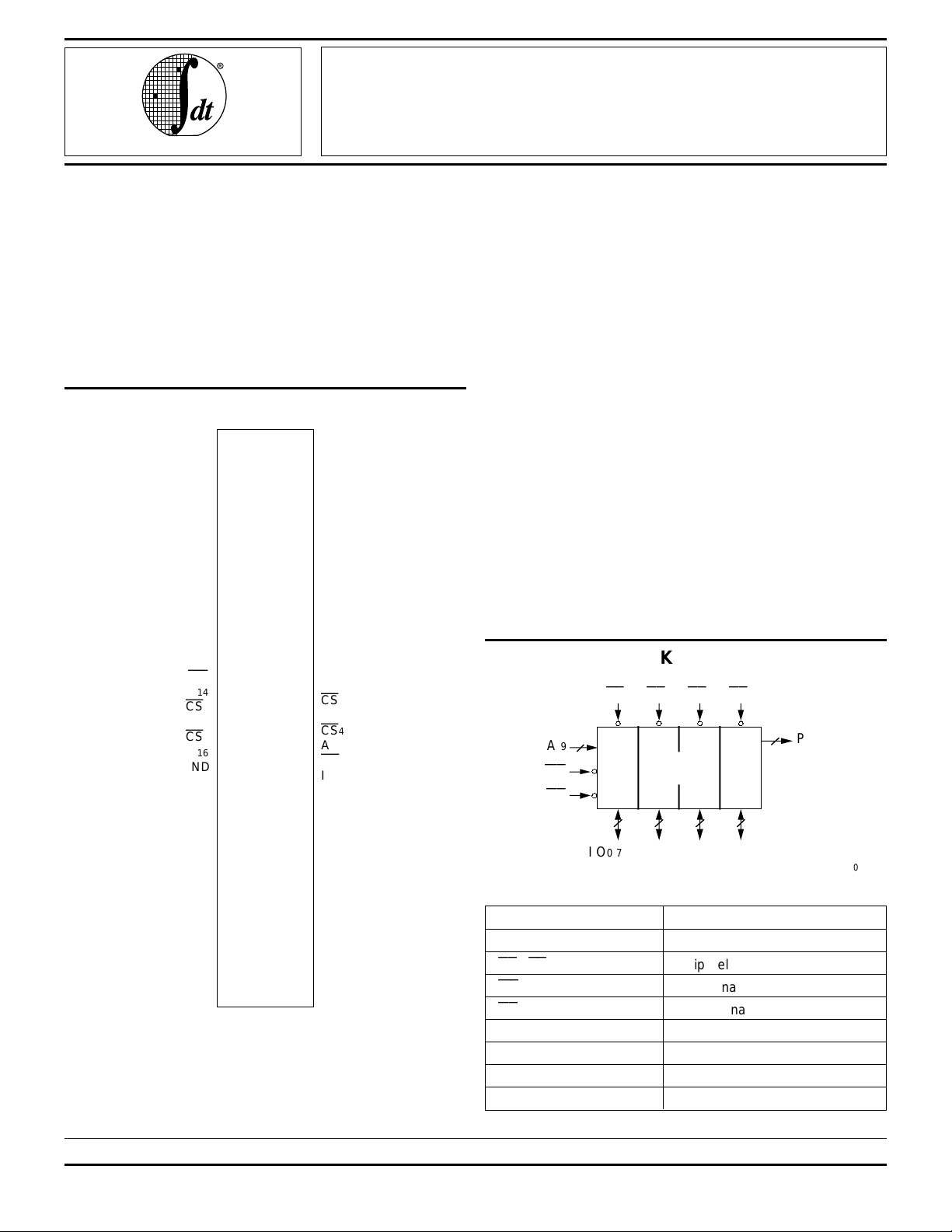
FUNCTIONAL BLOCK DIAGRAM
A0 – A19
WE
OE
CS1CS2CS3CS
20
1M x 32
RAM
8
8 8 8
I/O0-7
8-15 I/O16-23 I/O24-31
I/O
4
3
PD0 – PD3
3019 drw 02
PIN NAMES
I/O0–I/O31 Data Inputs/Outputs
A0–A19 Addresses
CS1–CS
WE
OE
PD0–PD3 Depth Identification
VCC Power
GND Ground
NC No Connect
4 Chip Selects
Write Enable
Output Enable
3019 tbl 01
COMMERCIAL TEMPERATURE RANGE SEPTEMBER 1996
1996 Integrated Device Technology, Inc. DSC-3019/5
7.07 1
Page 2
IDT7MP4120
1M x 32 CMOS STATIC RAM MODULE COMMERCIAL TEMPERATURE RANGE
CAPACITANCE (TA = +25°C, F = 1.0MHz)
Symbol Parameter
CI/O Data I/O Capacitance V(IN) = 0V 15 pF
IN1 Input Capacitance V(IN) = 0V 60 pF
C
(Address)
IN2 Input Capacitance V(IN) = 0V 75 pF
C
(WE, OE)
IN3 Input Capacitance (
C
NOTE: 3019 tbl 02
1. This parameter is guaranteed by design but not tested.
(1)
Conditions Max. Unit
CS
)V(IN) = 0V 20 pF
RECOMMENDED DC OPERATING
CONDITIONS
Symbol Parameter Min. Typ. Max. Unit
VCC Supply Voltage 4.5 5.0 5.5 V
GND Supply Voltage 0 0 0 V
VIH Input High Voltage 2.2 — 6.0 V
IL Input Low Voltage –0.5
V
NOTE: 3019 tbl 03
1. VIL (min) = –1.5V for pulse width less than 10ns.
(1)
— 0.8 V
TRUTH TABLE
Mode
Standby H X X High-Z Standby
Read L L H DATAOUT Active
Write L X L DATAIN Active
Read L H H High-Z Active
ABSOLUTE MAXIMUM RATINGS
Symbol Rating Value Unit
TERM Terminal Voltage with –0.5 to +7.0 V
V
TA Operating Temperature 0 to +70 °C
TBIAS Temperature Under Bias –10 to +85 °C
TSTG Storage Temperature –55 to +125 °C
OUT DC Output Current 50 mA
I
NOTE: 3019 tbl 06
1. Stresses greater than those listed under ABSOLUTE MAXIMUM
RATINGS may cause permanent damage to the device. This is a stress
rating only and functional operation of the device at these or any other
conditions above those indicated in the operational sections of this
specification is not implied. Exposure to absolute maximum rating
conditions for extended periods may affect reliability.
CSCSOEOEWE
Respect to GND
WE
Output Power
3019 tbl 05
(1)
RECOMMENDED OPERATING
TEMPERATURE AND SUPPLY VOLTAGE
Ambient
Grade Temperature GND VCC
Commercial 0°C to +70°C 0V 5.0V ± 10%
3019 tbl 04
DC ELECTRICAL CHARACTERISTICS
(VCC = 5.0V ±10%, TA = 0°C to +70°C)
Symbol Parameter Test Conditions Min. Max. Unit
LI| Input Leakage VCC = Max.; VIN = GND to VCC —80µA
|I
(Address and Control)
|ILI| Input Leakage (Data) VCC = Max.; VIN = GND to VCC —10µA
|ILO| Output Leakage VCC = Max.; CS = VIH, VOUT = GND to VCC —10µA
VOL Output LOW VCC = Min., IOL = 8mA — 0.4 V
OH Output HIGH VCC = Min., IOH = –4mA 2.4 — V
V
3019 tbl 07
7MP4120
Symbol Parameter Test Conditions Max. Unit
CC Dynamic Operating f = fMAX;
I
Current V
SB Standby Supply
I
CS
Current Outputs Open, f = f
ISB1 Full Standby
CS
Supply Current V
CS
= VIL 1280 mA
CC = Max.; Output Open
≥ VIH, VCC = Max. 480 mA
MAX
≥ VCC – 0.2V; f = 0 120 mA
IN > VCC – 0.2V or < 0.2V
3019 tbl 08
7.07 2
Page 3
IDT7MP4120
1M x 32 CMOS STATIC RAM MODULE COMMERCIAL TEMPERATURE RANGE
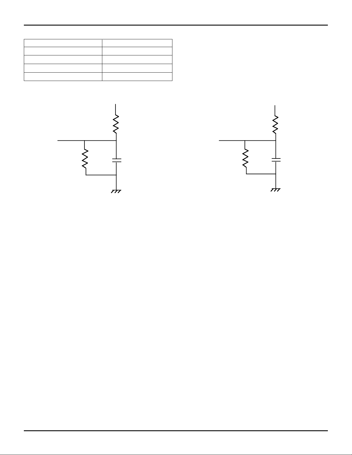
AC TEST CONDITIONS
Input Pulse Levels GND to 3.0V
Input Rise/Fall Times 5ns
Input Timing Reference Levels 1.5V
Output Reference Levels 1.5V
Output Load See Figures 1 and 2
2769 tbl 09
DATA
OUT
255Ω
Figure 1. Output Load
+5 V
480 Ω
30 pF*
3019 drw 03
*Includes scope and jig.
DATA
OUT
255Ω
Figure 2. Output Load
OLZ,tOHZ, tCHZ, tCLZ, tWHZ, tOW)
(for t
+5 V
480 Ω
5 pF*
3019 drw 04
7.07 3
Page 4

IDT7MP4120
1M x 32 CMOS STATIC RAM MODULE COMMERCIAL TEMPERATURE RANGE
AC ELECTRICAL CHARACTERISTICS
(VCC = 5V ±10%, TA = 0°C to +70°C)
7MP4120SxxZ/M
–20 –25
Symbol Parameter Min. Max. Min. Max. Unit
Read Cycle
tRC Read Cycle Time 20 — 25 — ns
tAA Address Access Time — 20 — 25 ns
tACS Chip Select Access Time — 20 — 25 ns
(1)
tCLZ
tOE Output Enable to Output Valid — 12 — 15 ns
tOLZ
tCHZ
tOHZ
tOH Output Hold from Address Change 3 — 3 — ns
(1)
tPU
(1)
tPD
Write Cycle
tWC Write Cycle Time 20 — 25 — ns
tCW Chip Select to End-of-Write 17 — 20 — ns
tAW Address Valid to End-of-Write 17 — 20 — ns
tAS Address Set-up Time 0 — 0 — ns
tWP Write Pulse Width 15 — 20 — ns
tWR Write Recovery Time 3 — 3 — ns
tWHZ
tDW Data to Write Time Overlap 12 — 15 — ns
tDH Data Hold from Write Time 0 — 0 — ns
OW
t
NOTE: 3019 tbl 10
1. This parameter is guaranteed by design, but not tested.
Chip Select to Output in Low-Z 3 — 3 — ns
(1)
Output Enable to Output in Low-Z 0 — 0 — ns
(1)
Chip Deselect to Output in High-Z — 10 — 12 ns
(1)
Output Disable to Output in High-Z — 10 — 12 ns
Chip Select to Power-Up Time 0 — 0 — ns
Chip Deselect to Power-Down Time — 20 — 25 ns
(1)
Write Enable to Output in High-Z — 10 — 15 ns
(1)
Output Active from End-of-Write 0 — 0 — ns
7.07 4
Page 5

IDT7MP4120
1M x 32 CMOS STATIC RAM MODULE COMMERCIAL TEMPERATURE RANGE
TIMING WAVEFORM OF READ CYCLE NO. 1
ADDRESS
t
AA
OE
CS
t
ACS
(5)
t
CLZ
DATA
OUT
TIMING WAVEFORM OF READ CYCLE NO. 2
ADDRESS
tAA
(1)
t
RC
t
(1,2,4)
tRC
OLZ
(5)
t
OE
t
CHZ
t
OHZ
(5)
t
OH
(5)
3019 drw 05
tOH tOH
DATAOUT
TIMING WAVEFORM OF READ CYCLE NO. 3
PREVIOUS DATA VALID
(1,3,4)
CS
tACS
(5)
tCLZ
DATAOUT
NOTES:
1.WE is HIGH for Read Cycle.
2. Device is continuously selected. CS = V
3. Address valid prior to or coincident with CS transition LOW.
4.OE = V
5. Transition is measured ±200mV from steady state. This parameter is guaranteed by design, but not tested.
IL.
IL.
DATA VALID
tCHZ
3019 drw 06
(5)
3019 drw 07
7.07 5
Page 6

IDT7MP4120
1M x 32 CMOS STATIC RAM MODULE COMMERCIAL TEMPERATURE RANGE
TIMING WAVEFORM OF WRITE CYCLE NO. 1 (
tWC
ADDRESS
OE
tAW
CS
(7)
tWP
DATA
DATA
WE
OUT
tAS tWR
(6)
tWHZ
(6)
tOHZ
(4)
IN
WEWE CONTROLLED)
(6)
tOW
tDW
DATA VALID
(1, 2, 3, 7)
tDH
(6)
tOHZ
(4)
3019 drw 08
TIMING WAVEFORM OF WRITE CYCLE NO. 2 (
CSCS CONTROLLED)
(1, 2, 3, 5)
tWC
ADDRESS
tAW
CS
tAS tWR
tCW
WE
tDW
DATAIN
NOTES:
1.WE or CS must be HIGH during all address transitions.
2. A write occurs during the overlap (t
WR is measured from the earlier of
3. t
4. During this period, I/O pins are in the output state, and input signals must not be applied.
5. If the CS LOW transition occurs simultaneously with or after the WE LOW transition, the outputs remain in a high-impedance state.
6. Transition is measured ±200mV from steady state with a 5pF load (including scope and jig). This parameter is guaranteed by design, but not tested.
7. If OE is LOW during a WE controlled write cycle, the write pulse width must be the larger of t
to be placed on the bus for the required t
be as short as the specified t
WP.
WP) of a LOW
CS
or WE going HIGH to the end of write cycle.
DW. If
CS
and a LOW WE.
OE
is HIGH during a WE controlled write cycle, this requirement does not apply and the write pulse can
DATA VALID
WP or (tWHZ + tDW) to allow the I/O drivers to turn off and data
tDH
3019 drw 09
7.07 6
Page 7

IDT7MP4120
1M x 32 CMOS STATIC RAM MODULE COMMERCIAL TEMPERATURE RANGE
PACKAGE DIMENSIONS
ZIP VERSION
FRONT VIEW
SIDE VIEW
0.580
0.600
PIN 1
0.100 TYP
0.050 TYP
3.940
3.960
0.250 TYP
REAR VIEW
0.015
0.025
0.025 TYP
0.125
0.175
0.025 TYP
PIN 1
0.365 MAX
0.100 TYP
3019 drw 10
SIMM VERSION
0.640
0.660
0.240
0.260
0.070
0.090
PIN 1
4.240
4.260
FRONT VIEW
3.980
3.988
0.250
TYP.
0.050
TYP.
0.350
MAX.
0.390
0.410
0.045
0.055
SIDE VIEW
BACK VIEW
PIN 1
7.07 7
3019 drw 11
Page 8

IDT7MP4120
1M x 32 CMOS STATIC RAM MODULE COMMERCIAL TEMPERATURE RANGE
ORDERING INFORMATION
IDT
XXXXX
Device
Type
X
PowerXSpeedXPackage
X
Process/
Temperature
Range
Blank
Z
M
20
25
Commercial (0°C to +70°C)
FR-4 ZIP (Zig-Zag In-line vertical Package)
FR-4 SIMM (Single In-line Memory Module)
Speed in Nanoseconds
S Standard Power
7MP4120 1M x 32 Static RAM Module
3019 drw 12
7.07 8
 Loading...