

Datasheet IDT7MB4048S35P, IDT7MB4048S30P, IDT7MB4048S25P Datasheet (Integrated Device Technology)
Page 1
CSWEOE
OE
CS
WE
Integrated Device Technology, Inc.
512K x 8
CMOS STATIC RAM MODULE
IDT7MB4048
FEATURES:
• High-density 4-megabit (512K x 8) Static RAM module
• Fast access time: 25ns (max.)
Surface mounted plastic packages on a 32-pin, 600 mil
FR-4 DIP substrate
• Single 5V (±10%) power supply
• Inputs/outputs directly TTL-compatible
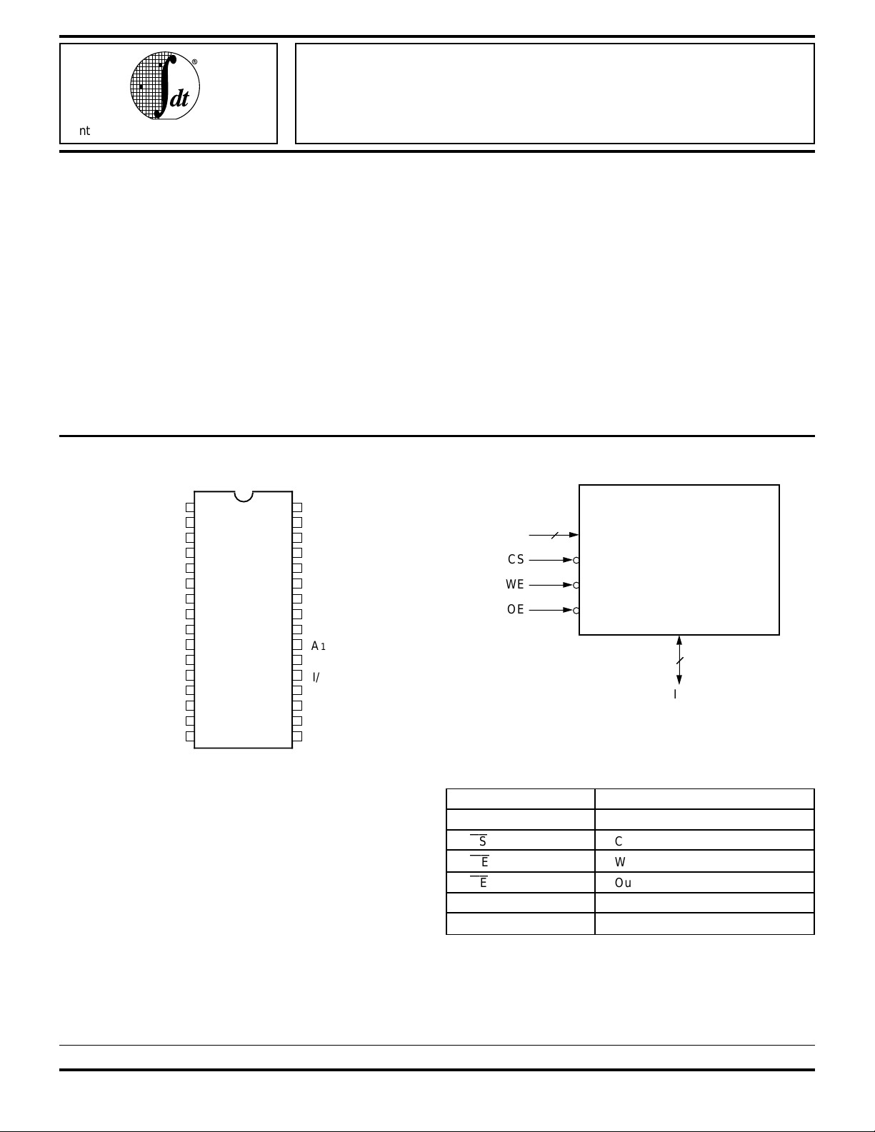
PIN CONFIGURATION
A
A
A
A
A
A
A
A
A
A
A
A
I/O
I/O
I/O
GND
1
18
2
16
3
14
4
12
5
7
6
6
7
5
8
4
9
3
10
2
11
1
12
0
13
0
14
1
15
2
16
DIP
TOP VIEW
32
Vcc
31
A
A
A
A
A
A
A
I/O
I/O
I/O
I/O
I/O
15
17
13
8
9
11
10
7
6
5
4
3
2675 drw 01
30
29
28
27
26
25
24
23
22
21
20
19
18
17
DESCRIPTION:
The IDT7MB4048 is a 4-megabit (512K x 8) Static RAM
module constructed on a multilayer epoxy laminate (FR-4)
substrate using four 1 megabit SRAMs and a decoder. The
IDT7MB4048 is available with access times as fast as 25ns.
The IDT7MB4048 is packaged in a 32-pin FR-4 DIP resulting
in the JEDEC footprint in a package 1.6 inches long and 0.6
inches wide.
All inputs and outputs of the IDT7MB4048 are TTL-compatible and operate from a single 5V supply. Fully asynchronous circuitry requires no clocks or refresh for operation and
provides equal access and cycle times for ease of use.
FUNCTIONAL BLOCK DIAGRAM
ADDRESS
19
512K x 8
RAM
8
I/O
2675 drw 02
PIN NAMES
I/O0-7 Data Inputs/Outputs
0-18 Addresses
A
CS
WE
OE
CC Power
V
GND Ground
Chip Select
Write Enable
Output Enable
2675 tbl 01
The IDT logo is a registered trademark of Integrated Device Technology Inc.
COMMERCIAL TEMPERATURE RANGE DECEMBER 1995
©1996 Integrated Device Technology, Inc. DSC-2675/6
7.11 1
Page 2
IDT7MB4048
512K x 8 CMOS STATIC RAM MODULE COMMERCIAL TEMPERATURE RANGE
TRUTH TABLE
CSCS
OEOE
Mode
CS
CSCS
OE
OEOE
WEWE
WE
WEWE
Output Power
Standby H X X High-Z Standby
Read L L H D
OUT Active
Read L H H High-Z Active
Write L X L D
CAPACITANCE
(1)
(TA = +25°C, f = 1.0MHz)
IN Active
2675 tbl 02
Symbol Parameter Conditions Typ. Unit
IN Input Capacitance VIN = 0V 35 pF
C
C
IN(C) Input Capacitance (
C
OUT Output Capacitance VOUT = 0V 35 pF
NOTE: 2675 tbl 03
1. This parameter is guaranteed by design, but not tested.
CS
)VIN = 0V 8 pF
RECOMMENDED DC OPERATING CONDITIONS
Symbol Parameter Min. Typ. Max. Unit
CC Supply Voltage 4.5 5 5.5 V
V
GND Supply Voltage 0 0 0 V
IH Input High Voltage 2.2 — 6 V
V
IL Input Low Voltage –0.5
V
NOTE: 2675 tbl 04
1. VIL = –2.0V for pulse width less than 10ns.
(1)
— 0.8 V
ABSOLUTE MAXIMUM RATINGS
(1)
Symbol Rating Commercial Unit
V
TERM Terminal Voltage –0.5 to +7.0 V
with Respect
to GND
T
A Operating 0 to +70 °C
Temperature
BIAS Temperature –10 to +85 °C
T
Under Bias
T
STG Storage –55 to +125 °C
Temperature
OUT DC Output Current 50 mA
I
NOTE: 2675 tbl 05
1. Stresses greater than those listed under ABSOLUTE MAXIMUM RAT-
INGS may cause permanent damage to the device. This is a stress rating
only and functional operation of the device at these or any other conditions
above those indicated in the operational sections of this specification is
not implied. Exposure to absolute maximum rating conditions for ex-
tended periods may affect reliability.
RECOMMENDED OPERATING
TEMPERATURE AND SUPPLY VOLTAGE
Ambient
Grade Temperature GND V
Commercial 0°C to +70°C 0V 5V ± 10%
CC
2675 tbl 06
DC ELECTRICAL CHARACTERISTICS
(VCC = 5V ± 10%, TA = 0°C to +70°C)
7MB4048SxxP
Symbol Parameter Test Conditions Min. Max. Unit
|ILI| Input Leakage VCC = Max., VIN = GND to VCC —8µA
LO| Output Leakage VCC = Max.,
|I
VOUT = GND to VCC
VOL Output Low Voltage VCC = Min., IOL = 8mA — 0.4 V
VOH Output High Voltage VCC = Min., IOH = –1mA 2.4 — V
CC Dynamic Operating Current VCC = Max.,
I
Outputs Open
SB Standby Supply Current
I
CS
≥ VIH, VCC = Max., f = fMAX,
(TTL Levels) Outputs Open
SB1 Full Standby Supply Current
I
CS
≥ VCC - 0.2V, VIN ≥ VCC - 0.2V — 170 mA
(CMOS Levels) or ≤ 0.2
CS
= VIH,—8µA
CS
≤ VIL; f = fMAX, — 480 mA
250 mA
—
2675 tbl 07
7.11 2
Page 3

IDT7MB4048
512K x 8 CMOS STATIC RAM MODULE COMMERCIAL TEMPERATURE RANGE
AC TEST CONDITIONS
Input Pulse Levels GND to 3.0V
Input Rise/Fall Times 5ns
Input Timing Reference Levels 1.5V
Output Reference Levels 1.5V
Output Load See Figures 1 & 2
2675 tbl 09
+5 V
480 Ω
5 pF*
2675 drw 05
DATA
OUT
255Ω
Figure 1. Output Load
+5 V
480 Ω
30 pF*
2675 drw 04
DATA
OUT
255Ω
Figure 2. Output Load
OLZ, tCHZ, tOHZ, tWHZ, tOW and tCLZ)
(for t
AC ELECTRICAL CHARACTERISTICS
(VCC = 5V ± 10%, TA = 0°C to +70°C)
7MB4048
–25 –30 –35
Symbol Parameter Min. Max. Min. Max. Min. Max. Unit
Read Cycle
tRC Read Cycle Time 25 — 30 — 35 — ns
tAA Address Access Time — 25 — 30 — 35 ns
tACS Chip Select Access Time — 25 — 30 — 35 ns
tOE Output Enable to Output Valid — 12 — 15 — 15 ns
(1)
tOHZ
tOLZ
tCLZ
tCHZ
tOH Output Hold from Address Change 3 — 3 — 3 — ns
tPU
tPD
Write Cycle
tWC Write Cycle Time 25 — 30 — 35 — ns
tWP Write Pulse Width 17 — 20 — 25 — ns
tAS
tAW Address Valid to End-of-Write 20 — 25 — 30 — ns
tCW Chip Select to End-of-Write 20 — 25 — 30 — ns
tDW Data to Write Time Overlap 15 — 17 — 20 — ns
tDH
tWR
tWHZ
OW
t
NOTES 2675 tbl 10
1. This parameter is guaranteed by design, but not tested.
2. t
Output Disable to Output in High-Z — 12 — 12 — 15 ns
(1)
Output Enable to Output in Low-Z 0 — 0 — 0 — ns
(1)
Chip Select to Output in Low-Z 5 — 5 — 5 — ns
(1)
Chip Deselect to Output in High-Z — 14 — 16 — 20 ns
(1)
Chip Select to Power-Up Time 0 — 0 — 0 — ns
(1)
Chip Deselect to Power-Down Time — 25 — 30 — 35 ns
(2)
Address Set-up Time 3 — 0 — 0 — ns
(2)
Data Hold Time 0 — 0 — 0 — ns
(2)
Write Recovery Time 0 — 0 — 0 — ns
(1)
Write Enable to Output in High-Z — 15 — 15 — 15 ns
(1)
Output Active from End-of-Write 2 — 5 — 5 — ns
AS=0ns for
CS
controlled write cycles. tDH, tWR= 3ns for CS controlled write cycles.
7.11 3
Page 4

IDT7MB4048
OE
CS
CS
512K x 8 CMOS STATIC RAM MODULE COMMERCIAL TEMPERATURE RANGE
TIMING WAVEFORM OF READ CYCLE NO. 1
ADDRESS
t
AA
(5)
t
OLZ
t
ACS
(5)
t
CLZ
DATA
OUT
TIMING WAVEFORM OF READ CYCLE NO. 2
(1)
t
RC
t
(1, 2, 4)
t
RC
OE
t
CHZ
(5)
t
OH
t
OHZ
(5)
2675 drw 06
ADDRESS
t
AA
t
OH
DATA
OUT
TIMING WAVEFORM OF READ CYCLE NO. 3
t
ACS
t
CLZ
DATA
OUT
(1, 3, 4)
t
t
CHZ
OH
2675 drw 07
(5)(5)
2675 drw 08
NOTES:
1.WE is HIGH for Read Cycle.
2. Device is continuously selected, CS = V
3. Address valid prior to or coincident with CS transition LOW.
4.OE = V
5. Transition is measured ±200mV from steady state. This parameter is guaranteed by design, but not tested.
IL.
IL.
7.11 4
Page 5

IDT7MB4048
CS
WE
OE
CS
WE
512K x 8 CMOS STATIC RAM MODULE COMMERCIAL TEMPERATURE RANGE
TIMING WAVEFORM OF WRITE CYCLE NO. 1 (
t
WC
ADDRESS
t
AW
t
WP
DATA
DATA
OUT
IN
t
AS
(6)
t
WHZ
(6)
t
OHZ
(4)
WEWE
WE
CONTROLLED TIMING)
WEWE
(7)
t
DW
t
OW
(6)
t
t
DH
DATA VALID
WR
(1, 2, 3, 7)
(4)
t
OHZ
(6)
2675 drw 09
TIMING WAVEFORM OF WRITE CYCLE NO. 2 (
t
WC
CSCS
CS
CONTROLLED TIMING)
CSCS
(1, 2, 3, 5)
ADDRESS
t
AW
t
AS
DATA
IN
NOTES:
1.WE or CS must be HIGH during all address transitions.
2. A write occurs during the overlap (t
WR is measured from the earlier of
3. t
4. During this period, I/O pins are in the output state, and input signals must not be applied.
5. If the CS LOW transition occurs simultaneously with or after the WE LOW transition, the outputs remain in a high-impedance state.
6. Transition is measured ±200mV from steady state with a 5pF load (including scope and jig). This parameter is guaranteed by design, but not tested.
7. If OE is LOW during a WE controlled write cycle, the write pulse width must be the larger of t
to be placed on the bus for the required t
be as short as the specified t
WP.
WP) of a LOW
CS
or WE going HIGH to the end of write cycle.
DW. If
CS
and a LOW WE.
OE
is HIGH during a WE controlled write cycle, this requirement does not apply and the write pulse can
t
CW
t
DW
DATA VALID
WP or (tWHZ + tDW) to allow the I/O drivers to turn off and data
t
WR
t
DH
2675 drw 10
7.11 5
Page 6

IDT7MB4048
512K x 8 CMOS STATIC RAM MODULE COMMERCIAL TEMPERATURE RANGE
PACKAGE DIMENSIONS
1.590
1.610
0.600
0.620
TOP VIEW
Pin 1
0.035
0.065
0.015
0.025
BOTTOM VIEW
ORDERING INFORMATION
IDT
XXXX
Device
Type
A
Power
999
SpeedAPackageAProcess/
(1)
0.100
TYP.
Temperature
Range
0.120
0.175
0.360
MAX.
0.007
0.013
SIDE VIEW
0.590
0.620
2675 drw 11
Blank Commercial (0°C to +70°C)
P
25
30
35
S Standard Power
7MB4048 512K x 8 Static RAM Module (FR-4 substrate)
7.11 6
SOJs mounted on an FR-4 DIP
Speed in Nanoseconds
2675 drw 12
 Loading...