

Datasheet IDT7M1024S30GB, IDT7M1024S25GB, IDT7M1024S25G, IDT7M1024S20G Datasheet (Integrated Device Technology)
Page 1
Integrated Device Technology, Inc.
4K x 36 BiCMOS
SYNCHRONOUS DUAL-PORT
STATIC RAM MODULE
IDT7M1024
FEATURES:
• High-density 4K x 36 Synchronous Dual-Port SRAM
module
• Architecture based on Dual-Port RAM cells
— Allows full simultaneous access from both ports
• Synchronous operation
— 4ns set-up to clock, 1ns hold on all control, data, and
address inputs
— Data input, address, and control registers
— Fast 20ns clock to data out
— Self-timed write allows fast write cycle
• Clock enable feature
• Single 5V (±10%) power supply
• Multiple GND pins and decoupling capacitors for maximum noise immunity
• Inputs/outputs directly TTL-compatible
DESCRIPTION:
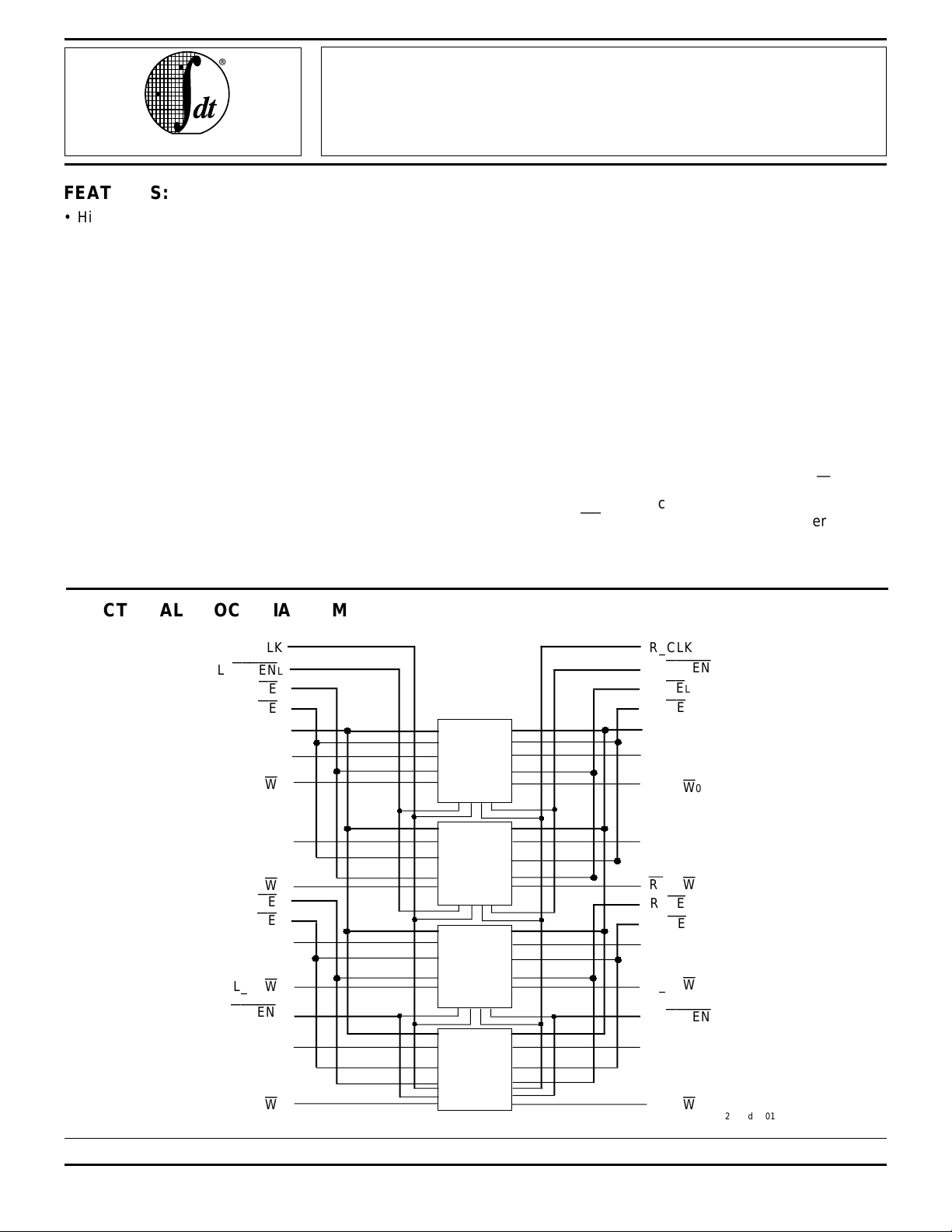
The IDT7M1024 is a 4K x 36 bit high-speed synchronous
Dual-Port Static RAM module constructed on a co-fired ce-
FUNCTIONAL BLOCK DIAGRAM
ramic substrate using four IDT7099 (4K x 9) Dual-Port RAMs.
The IDT7M1024 module is designed to be used as a standalone 36-bit Dual-Port Static RAM.
The IDT7M1024 provides a true synchronous Dual-Port
Static RAM interface. Registered inputs provide very short
set-up and hold times on address, data, and all critical control
inputs. All internal registers are clocked on the rising edge of
the clock signal. An asynchronous output enable is provided
to ease asynchronous bus interfacing.
The internal write pulse width is independent of the HIGH
and LOW periods of the clock. This allows the shortest
possible realized cycle times. Clock enable inputs are provided to stall the operation of the address and data input
registers without introducing clock skew for very fast interleaved memory applications.
The data inputs are gated to control on-chip noise in bussed
applications. The user must guarantee that the R/W pins are
LOW for at least one clock cycle before any write is attempted.
A HIGH on the CE input for one clock cycle will power down the
internal circuitry to reduce static power consumption.
The IDT7M1024 module is packaged in a 142-lead ceramic
L_
CLKEN
L_
CE
L_
OE
L_A0 – 11
L_I/O0 – 8
L_ R/
W
L_I/O9 – 17
L_ R/
W
L_
CE
L_
OE
L_I/O18 – 26
L_ R/
W
L_
CLKEN
L_I/O27 – 35
R_CLKL_CLK
R_
CLKEN
CE
L
OE
L
W
0
W
1
CE
H
OE
H
W
2
CLKEN
L
H
L
L
L
IDT7099
4K x 9
0
IDT7099
4K x 9
1
H
H
IDT7099
4K x 9
2
H
IDT7099
4K x 9
R_
R_
R_A0 – 11
R_I/O0 – 8
R_ R/
R_I/O9 – 17
R_ R/
R_
R_
R_I/O18 – 26
R_ R/
R_
R_I/O27 – 35
L_ R/
W
3
The IDT logo is a registered trademark of Integrated Device Technology, Inc.
R_ R/
W
3
2809 drw 01
MILITARY AND COMMERCIAL TEMPERATURE RANGES MARCH 1996
1996 Integrated Device Technology, Inc. DSC-2809/6
7.4 1
Page 2
IDT7M1024
4K x 36 BiCMOS SYNCHRONOUS DUAL-PORT STATIC RAM MODULE MILITARY AND COMMERCIAL TEMPERATURE RANGES
PGA (Pin Grid Array).
All IDT military modules are constructed with semiconductor components manufactured in compliance with the latest
revision of MIL-STD-883, Class B making them ideally suited
to applications demanding the highest level of performance
and reliability.
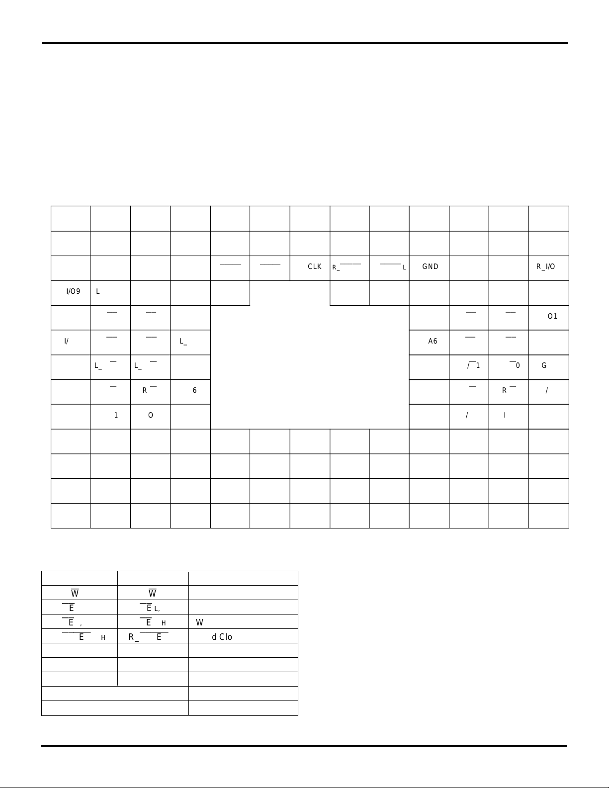
PIN CONFIGURATION
12345678910111213
A GND L_I/O3 L_I/O2 GND L_I/O1 L_I/O0 GND R_I/O0 R_I/O1 GND R_I/O2 R_I/O3 GND
B L_I/O4 L_I/O5 L_I/O6 L_A2 L_A1 L_A0 L_CLK R_A0 R_A1 R_A2 R_I/O6 R_I/O5 R_I/O4
C L_I/O8 VCC L_I/O7 GND
D L_I/O9 L_I/O10 L_I/O11 L_A3
E L_I/O12 L_CE LL_CE H L_A4 R_A5 R_CE HR_CE L R_I/O12
F L_I/O13 L_OE LL_OE H L_A5 R_A6 R_OE HR_OE L R_I/O13
G GND L_R/W0 L_R/W1 GND GND R_R/W1 R_R/W0 GND
H L_I/O14 L_R/W2 L_R/W3 L_A6 R_A7 R_R/W3 R_R/W2 R_I/O14
J L_I/O15 L_I/O16 L_I/O17 L_A7 R_A8 R_I/O17 R_I/O16 R_I/O15
K L_I/O20 L_I/O19 L_I/O18 G N D L_A10 L_A11 GND R_A11 R_A10 GND R_I/O18 R_I/O19 R_I/O20
L L_I/O21 VCC L_I/O22 L_A8 L_A9 L_I/O31 R_I/O35 R_I/O34 R_I/O30 R_A9 R_I/O22 VCC R_I/O21
M L_I/O23 L_I/O24 L_I/O25 L_I/O29 L_I/O30 L_I/O32 L_I/O35 R_I/O33 R_I/O31 R_I/O29 R_I/O25 R_I/O24 R_I/O23
N GND L_I/O26 L_I/O27 L_I/O28 GND L_I/O33 L_I/O34 R_I/O32
L_
CLKEN
GND
LL_
CLKEN
R_CLK
H
R_
CLKEN
GND
HR_
CLKEN
R_A3 R_A4 R_I/O11 R_I/O10 R_I/O9
GND
GND R_I/O7 VCC R_I/O8
L
R_I/O28 R_I/O27 R_I/O26 G N D
2809 drw 02
PIN NAMES
Left Port Right Port Names
L_R/W 0-3 R_R/W 0-3 Byte Read/Write Enables
L_OE L, H R_OE L, H Word Output Enables
L_CE L, H R_CE L, H Word Chip Enables
L_
CLKEN
L, H R_
L_CLK R_CLK Clock Inputs
L_A 0-11 R_A 0-11 Address Inputs
L_I/O 0-35 R_I/O 0-35 Data Input/Outputs
VCC Power
GND Ground
CLKEN
L, H Word Clock Enables
2809 tbl 01
7.4 2
Page 3
IDT7M1024
4K x 36 BiCMOS SYNCHRONOUS DUAL-PORT STATIC RAM MODULE MILITARY AND COMMERCIAL TEMPERATURE RANGES
ABSOLUTE MAXIMUM RATINGS
(1)
Symbol Rating Commercial Military Unit
(2)
V
TERM
Terminal Voltage –0.5 to +7.0 –0.5 to +7.0 V
with Respect to
GND
(3)
VTERM
T
Terminal Voltage –0.5 to VCC –0.5 to VCC V
A Operating 0 to +70 –55 to +125 °C
Temperature
BIAS Temperature –55 to +125 –65 to +135 °C
T
Under Bias
STG Storage –55 to +125 –65 to +150 °C
T
Temperature
OUT DC Output Current 50 50 mA
I
NOTES: 2809 tbl 02
1. Stresses greater than those listed under ABSOLUTE MAXIMUM RATINGS may cause permanent damage to the device. This is a stress rating
only and functional operation of the device at these or any other conditions
above those indicated in the operational sections of this specification is not
implied. Exposure to absolute maximum rating conditions for extended
periods may affect reliability.
2. Inputs and Vcc terminals only.
CAPACITANCE (TA = +25°C, F = 1.0MHZ)
Symbol Parameter
CIN Input Capacitance VIN = 0V 50 pF
OUT Output Capacitance VOUT = 0V 15 pF
C
(1)
Condition Max. Unit
2809 tbl 05
RECOMMENDED OPERATING
TEMPERATURE AND SUPPLY VOLTAGE
Ambient
Grade Temperature GND VCC
Military –55°C to +125°C 0V 5.0V ± 10%
Commercial 0°C to +70°C 0V 5.0V ± 10%
2809 tbl 03
RECOMMENDED DC OPERATING
CONDITIONS
Symbol Parameter Min. Typ. Max. Unit
VCC Supply Voltage 4.5 5.0 5.5 V
GND Supply Voltage 0 0 0 V
VIH Input HIGH Voltage 2.2 — 6.0 V
IL Input LOW Voltage –0.5
V
NOTE: 2809 tbl 04
1. VIL = -3.0V for pulse width less than 20ns.
(1)
— 0.8 V
TRUTH TABLES
TRUTH TABLE I: READ/WRITE CONTROL
Inputs
Synchronous Asynchronous Outputs
Clk
u
u
u
u
u
CE
CE
R/
W
W
OE
OE
h h X High-Z Deselected, Power Down, Data I/O Disabled
h l X DATAIN Deselected, Power Down, Data Input Enabled
l l X DATAIN Write
l h L DATAOUT Read
l h H High-Z Data I/O Disabled
(1)
I/O0-35 Mode
2809 tbl 06
TRUTH TABLE II:
CLOCK ENABLE FUNCTION TABLE
Inputs Register Inputs Register Outputs
Operating Mode Clk
Load “1”
Load “0”
Hold (do nothing)
NOTE: 2809 tbl 07
1. H = HIGH voltage level steady state, h = HIGH voltage level one set-up time prior to the LOW-to-HIGH clock transition, L =LOW voltage level steady state
l = LOW voltage level one set-up time prior to the LOW-to-HIGH clock transition, X = Don't care, N/C = No change
u
u
u
X H X X N/C N/C
(1)
CLKEN
CLKEN
ADDR DATAIN ADDR DATAOUT
lhhHH
lllLL
h X X N/C N/C
7.4 3
Page 4

IDT7M1024
4K x 36 BiCMOS SYNCHRONOUS DUAL-PORT STATIC RAM MODULE MILITARY AND COMMERCIAL TEMPERATURE RANGES
DC ELECTRICAL CHARACTERISTICS OVER THE
OPERATING TEMPERATURE AND SUPPLY VOLTAGE RANGE
Symbol Parameter Test Condition Min. Max. Unit
|ILI| Input Leakage Current VCC = 5.5V, VIN = 0V to VCC —40µA
|ILO| Output Leakage Current
VOL Output LOW Voltage IOL = 4mA — 0.4 V
OH Output HIGH Voltage IOH = –4mA 2.4 — V
V
CE
= VIH, VOUT = 0V to VCC —10µA
(VCC = 5.0V ± 10%)
IDT7M1024
2809 tbl 08
DC ELECTRICAL CHARACTERISTICS OVER THE
OPERATING TEMPERATURE AND SUPPLY VOLTAGE RANGE
Symbol Parameter Test Condition Version Typ. Max. Typ. Max. Typ. Max. Unit
CC Dynamic
I
Operating Outputs Open
Current (Both f = fM
Ports Active)
SB1 Standby L_
I
Current (Both R_CE ≥ V
Ports—TTL f = fMAX
Level Inputs)
SB2 Standby L_
I
Current (One Active Port
Port—TTL Outputs Open, Com’l. — 1080 — 1000 — —
Level Inputs) f = fMAX
ISB3 Full Standby Both Ports R_
Current (Both and L_CE ≥ V
Ports—CMOS V
Level Inputs) or VIN ≤ 0.2V, f = 0
ISB4 Full Standby One Port L_CE or R_CE ≥ Mil. — — — 1040 — 960 mA
Current (One V
Port—CMOS or V
Level Inputs) Outputs Open, f = fM
NOTES: 2809 tbl 09
1. At f = fMAX, address and control lines (except Output Enable) are cycling at the maximum frequency clock cycle of 1/tCLK, and using “AC TEST
CONDITIONS” of input levels of GND to 3V.
2. f = 0 means no address, clock, or control lines change. Applies only to inputs at CMOS level standby.
CE
≤ VIL Mil. — — — 1480 — 1440 mA
(1)
AX
CE
and Mil. — — — 680 — 560 mA
IH
(1)
CE
or R_CE ≥ VIH Mil. — — — 1080 — 1000 mA
(1)
CE
CC – 0.2V
IN ≥ VCC – 0.2V Com’l. — 80 — 80 — —
CC – 0.2V, VIN ≥ VCC – 0.2V
IN ≤ 0.2V, Active Port Com’l. — 1040 — 960 — —
(2)
(1)
AX
Com’l. — 1440 — 1360 — —
Com’l. — 720 — 640 — —
Mil. — — — 80 — 80 mA
(VCC = 5V ± 10%)
IDT7M1024SxxG, IDT7M1024SxxGB
–20 –25 –30
7.4 4
Page 5

IDT7M1024
4K x 36 BiCMOS SYNCHRONOUS DUAL-PORT STATIC RAM MODULE MILITARY AND COMMERCIAL TEMPERATURE RANGES
AC TEST CONDITIONS
Input Pulse Levels GND to 3.0V
Input Rise/Fall Times 3ns
Input Timing Reference Levels 1.5V
Output Reference Levels 1.5V
Output Load See Figures 1, 2 and 3
2909 tbl 10
DATA OUT
Zo = 50Ω
Figure 1. Output Load
50Ω
1.5V
2809 drw 03
5V
8
7
DATA
OUT
775Ω
1250Ω
∆TAA
(Typical, ns)
5pF*
6
5
4
3
2
1
2809 drw 04
Figure 2. Output Load (for t
*Including scope and jig.
CLZ, tCHZ, tOLZ, and tOHZ)
Figure 3. Lumped Capacitive Load, Typical Derating
20 40 10060 80 120140 160 180 200
Capacitance (pF)
2809 drw 05
AC ELECTRICAL CHARACTERISTICS OVER THE OPERATING TEMPERATURE RANGE —
(READ AND WRITE CYCLE TIMING)
(Commercial: VCC = 5V ± 10%, TA = 0°C to +70°C; Military: VCC = 5V ± 10%, TA = –55°C to +125°C)
7M1024SxxG, 7M1024SxxGB
–20 –25 –30
Symbol Parameter Min. Max. Min. Max. Min. Max. Unit
tCLK Clock Cycle Time 20 — 25 — 30 — ns
tCLKH Clock HIGH Time 8 — 10 — 12 — ns
tCLKL Clock LOW Time 8 — 10 — 12 — ns
tCQV Clock HIGH to Output Valid — 20 — 25 — 30 ns
tRSU Registered Signal Set-up Time 5 — 6 — 7 — ns
tRHD Registered Signal Hold Time 2 — 2 — 2 — ns
tCOH Data Output Hold After Clock HIGH 3 — 3 — 3 — ns
tCLZ Clock HIGH to Output Low-Z 2 — 2 — 2 — ns
tCHZ Clock HIGH to Output High-Z 2 9 2 12 2 15 ns
tOE Output Enable to Output Valid — 10 — 12 — 15 ns
tOLZ Output Enable to Output Low-Z 0 — 0 — 0 — ns
tOHZ Output Disable to Output High-Z — 9 — 11 — 14 ns
tCSU Clock Enable, Disable Set-up Time 5 — 6 — 7 — ns
tCHD Clock Enable, Disable Hold Time 3 — 3 — 3 — ns
Port-to-Port Delay
CWDD Write Port Clock HIGH to Read Data Delay — 35 — 45 — 55 ns
t
2809 tbl 11
7.4 5
Page 6

IDT7M1024
4K x 36 BiCMOS SYNCHRONOUS DUAL-PORT STATIC RAM MODULE MILITARY AND COMMERCIAL TEMPERATURE RANGES
TIMING WAVEFORM OF READ CYCLE, EITHER SIDE
tCLK
CLOCK
CLKEN
CE
R/
ADDRESS
OUT
DATA
OE
tRSU
W
tCLKH tCLKL
tRHD
An An + 1 An + 2 An + 3
tCQV tCOH
Qn Qn + 1 Qn + 1
tCLZ
(1,2)
tCSU tCHD tCSU
tOHZ
tCHZ
tOLZ
tOE
2809 drw 06
TIMING WAVEFORM OF READ CYCLE WITH PORT-TO-PORT DELAY
CLOCKR
R/
W
R
ADDRR
DATA INR
CLOCKL
R/
W
ADDRL
MATCH
VALID
L
MATCH
tCWDD tCQV
NO
MATCH
MATCH
NO
DATA OUTL
NOTES:
1. L_CE = R_CE = L, L_
2.OE = L for the reading port.
CLKEN
= R_
CLKEN
= L
VALID
VALID
tCOH
2809 drw 07
7.4 6
Page 7

IDT7M1024
4K x 36 BiCMOS SYNCHRONOUS DUAL-PORT STATIC RAM MODULE MILITARY AND COMMERCIAL TEMPERATURE RANGES
TIMING WAVEFORM OF READ-TO-WRITE CYCLE No. 1, CE HIGH
CLOCK
CLKEN
CE
R/
W
ADDRESS
IN
DATA
DATAOUT
NOTE:
1.OE LOW throughout.
tCLK
tCLKH tCLKL
tCLKH tCLKL
An An + 1 An + 2 An + 3
tCQV tCHZ
Qn
tCLZ
tCLK
tRSU
Dn + 2 Dn + 3
(1)
tRHD
2809 drw 08
TIMING WAVEFORM OF READ-TO-WRITE CYCLE NO. 1,
tCLK
CLOCK
CLKEN
CE
R/
W
ADDRESS
DATA
DATAOUT
IN
tCLKH tCLKL
An An + 1 An + 1 An + 2
tCQV tCHZ
Qn
tCLZ
CECE LOW
tRSU
(1,2)
tRHD
Dn + 1 Dn + 2
2809 drw 09
NOTES:
1. During dead cycle, if CE is LOW, data will be written into array.
2.OE LOW throughout.
7.4 7
Page 8

IDT7M1024
4K x 36 BiCMOS SYNCHRONOUS DUAL-PORT STATIC RAM MODULE MILITARY AND COMMERCIAL TEMPERATURE RANGES
PACKAGE DIMENSIONS
1.327
1.353
PIN A1
TOP VIEW
1.327
1.353
0.125
0.135
SIDE VIEW
0.045
0.055
0.015
0.021
0.100 TYP
0.195 MAX
0.050 TYP
ORDERING INFORMATION
IDT
XXXX
Device
Type
A
Power
999
SpeedAPackage
BOTTOM VIEW
Temperature
A
Process/
Range
2809 drw 10
BlankBCommercial (0°C to +70°C)
Military (–55°C to +125°C)
Compliant to MIL-STD-883, Class B
G Ceramic Pin Grid Array
20
25
30
S Standard Power
7M1024 4K x 36-Bit Synchronous Dual-Port RAM Module
Commercial Only
Military Only
Speed in Nanoseconds
2809 drw 11
7.4 8
 Loading...