

Datasheet IDT7M1003S50CB, IDT7M1003S40CB, IDT7M1003S40C, IDT7M1003S35C, IDT7M1001S40CB Datasheet (Integrated Device Technology)
...Page 1

FEATURES
• High-density 1M/512K CMOS Dual-Port Static RAM
module
• Fast access times:
—Commercial 35, 40ns
—Military 40, 50ns
• Fully asynchronous read/write operation from either port
• Full on-chip hardware support of semaphore signaling
between ports
• Surface mounted LCC (leadless chip carriers) components on a 64-pin sidebraze DIP (Dual In-line Package)
• Multiple Vcc and GND pins for maximum noise immunity
• Single 5V (±10%) power supply
• Input/outputs directly TTL-compatible
DESCRIPTION:
The IDT7M1001/IDT7M1003 is a 128K x 8/64K x 8 highspeed CMOS Dual-Port Static RAM module constructed on a
multilayer ceramic substrate using eight IDT7006 (16K x 8)
Dual-Port RAMs and two IDT FCT138 decoders or depopulated using only four IDT7006s and two decoders.
This module provides two independent ports with separate
control, address, and I/O pins that permit independent and
asynchronous access for reads or writes to any location in
memory. System performance is enhanced by facilitating
port-to-port communication via semaphore (
SEM
) “handshake” signaling. The IDT7M1001/1003 module is designed
to be used as stand-alone Dual-Port RAM where on-chip
hardware port arbitration is not needed. It is the users responsibility to ensure data integrity when simultaneously
accessing the same memory location from both ports.
The IDT7M1001/1003 module is packaged on a multilayer
co-fired ceramic 64-pin DIP (Dual In-line Package) with dimensions of only 3.2" x 0.62" x 0.38". Maximum access times
as fast as 35ns over the commercial temperature range are
available.
All inputs and outputs of the IDT7M1001/1003 are TTLcompatible and operate from a single 5V supply. Fully asynchronous circuitry is used, requiring no clocks or refreshing for
operation of the module.
All IDT military module semiconductor components are
manufacured in compliance with the latest revision of MILSTD-883, Class B, making them ideally suited to applications
demanding the highest level of performance and reliability.
128K x 8
64K x 8
CMOS DUAL-PORT
STATIC RAM MODULE
IDT7M1001
IDT7M1003
Left Port Right Port Description
A (0–16)L A (0–16)R Address Inputs
I/O (0–7)L I/O (0–7)R Data Inputs/Outputs
R/
W
L R/WR Read/Write Enables
CS
L
CS
R Chip Select
OE
L
OE
R Output Enable
SEM
L
SEM
R Semaphore Control
VCC Power
GND Ground
2804 tbl 01
PIN CONFIGURATION
(1)
MILITARY AND COMMERCIAL TEMPERATURE RANGES MARCH 1995
1995 Integrated Device Technology, Inc. DSC-7066/5
7.5 1
The IDT logo is a registered trademark of Integrated Device Technology, Inc.
PIN NAMES
DIP
TOP VIEW
CS
W
OE
CS
W
OE
SEM
SEM
2804 drw 01
Integrated Device Technology, Inc.
CC
R/
L
L
L
L
A
0L
A1L
GND
A2L
A3L
A4L
A5L
A6L
A7L
A8L
A9L
A10L
NOTE:
1. For the IDT7M1003 (64K x 8) version, Pins 23 and 43 must be connected
to GND for proper operation of the module.
A11L
A12L
A
13L
A14L
A15L
A16L GND
I/O0L
I/O1L
I/O2L
I/O3L
I/O4L
I/O5L
I/O6L
I/O7L
GND
1
2
3
4
5
6
7
8
9
10
11
12
13
14
15
16
17
18
19
20
21
22
23
24
25
26
27
28
29
30
31
32
64V
63
62
61
60
59
58
57
56
55
54
53
52
51
50
49
48
47
46
45
44
43
42
41
40
39
38
37
36
35
34
33
GND
R/
R
R
A0R
A1R
A2R
A3R
A4R
A5R
A6R
A7R
A8R
A9R
A10R
A11R
A12R
A13R
A14R
15R
A
A16R
I/O0R
I/O1R
I/O2R
I/O3R
I/O4R
I/O5R
I/O6R
I/O7R
VCC
R
R
Page 2
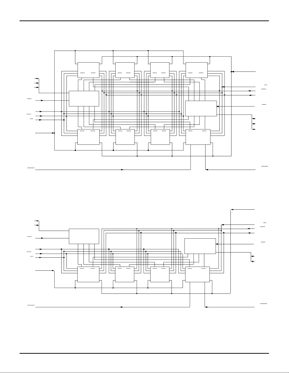
IDT7M1001/1003
L_I/O0-7
R_I/O0-7
R_A0-13
L_I/O0-7
R_I/O0-7
R_A0-13
128K/64K x 8 CMOS DUAL-PORT STATIC RAM MODULE MILITARY AND COMMERCIAL TEMPERATURE RANGES
FUNCTIONAL BLOCK DIAGRAM
7M1001
L_A16
L_A15
L_A14
L_CS
L_A0-13
L_OE
L_R/W
L_SEM
74FCT138
L CS RCS
7006
7025
CS CSL R CS CSL RL CS RCS L CS RCS
CS CS
L R
7006
CS CS
L R
7006
700670067006 7006
74FCT138
7006
R_R/W
R_OE
R_CS
R_A14
R_A15
R_A16
RCSL CS
R_SEM
2804 drw 02
7M1003
L_A15
L_A14
L_CS
L_A0-13
L_OE
L_R/W
L_SEM
74FCT138
L CS RCS
7006
L R
CS CS
7006
CS CS
L R
7006
74FCT138
7006
R_R/W
R_OE
R_CS
R_A14
R_A15
RCSL CS
R_SEM
2804 drw 03
7.5 2
Page 3
IDT7M1001/1003
128K/64K x 8 CMOS DUAL-PORT STATIC RAM MODULE MILITARY AND COMMERCIAL TEMPERATURE RANGES
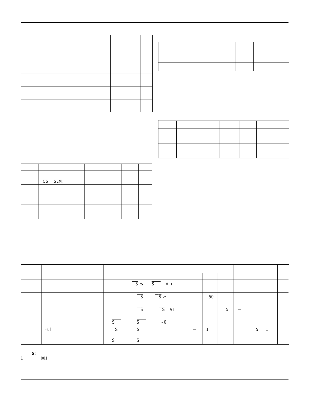
ABSOLUTE MAXIMUM RATINGS
(1)
Symbol Rating Commercial Military Unit
TERM Terminal Voltage –0.5 to +7.0 –0.5 to +7.0 V
V
with Respect to
GND
A Operating 0 to +70 –55 to +125 °C
T
Temperature
T
BIAS Temperature –55 to +125 –65 to +135 °C
Under Bias
T
STG Storage –55 to +125 –65 to +150 °C
Temperature
OUT DC Output 50 50 mA
I
Current
NOTE:
1. Stresses greater than those listed under ABSOLUTE MAXIMUM RATINGS
may cause permanent damage to the device. This is a stress rating only
and functional operation of the device at these or any other conditions
above those indicated in the operational sections of this specification is not
implied. Exposure to absolute maximum rating conditions for extended
periods may affect reliability.
CAPACITANCE
(1)
(TA = +25°C, f = 1.0MHz)
2804 tbl 02
Symbol Parameter Test Conditions Max. Unit
C
IN1 Input Capacitance VIN = 0V 15 pF
(CS or
SEM
)
CIN2 Input Capacitance VIN = 0V 100 pF
(Data, Address,
All Other Controls)
COUT Output Capacitance VOUT = 0V 100 pF
(Data)
NOTE:
1. This parameter is guaranteed by design but not tested.
2804 tbl 03
RECOMMENDED OPERATING
TEMPERATURE AND SUPPLY VOLTAGE
Ambient
Grade Temperature GND VCC
Military –55°C to +125°C 0V 5.0V ± 10%
Commercial 0°C to +70°C 0V 5.0V ± 10%
2804 tbl 04
RECOMMENDED DC OPERATING
CONDITIONS
Symbol Parameter Min. Typ. Max. Unit
VCC Supply Voltage 4.5 5.0 5.5 V
GND Supply Voltage 0 0 0 V
VIH Input High Voltage 2.2 - 6.0 V
IL Input Low Voltage –0.5
V
NOTE:
1. V
IL (min.) = –3.0V for pulse width less than 20ns.
(1)b
b - 0.8 V
2804 tbl 05
DC ELECTRICAL CHARACTERISTICS
(VCC = 5V ± 10%, TA = –55°C to +125°C or 0°C to +70°C)
Commercial Military
(1)
Symbol Parameter Test Conditions Min. Max.
CC2 Dynamic Operating VCC = Max.,
I
CS
≤ VIL,
SEM
≥ VIH — 940 660 — 1130 790 mA
Max.
(2)
Min. Max.
Current (Both Ports Active) Outputs Open, f = fMAX
ICC1 Standby Supply VCC = Max., L_CS or R_CS ≥ VIH — 750 470 — 905 565 mA
Current (One Port Active) Outputs Open, f = fMAX
ISB1 Standby Supply VCC = Max., L_CS and R_CS ≥ VIH — 565 285 — 685 345 mA
Current (TTL Levels) Outputs Open, f = f
SB2 Full Standby Supply L_
I
Current (CMOS Levels) V
NOTES:
1. IDT7M1001 (128K x 8) version only.
2. IDT7M1003 (64K x 8) version only.
L_
SEM
and R_
CS
and R_CS ≥ VCC –0.2V — 125 65 — 245 125 mA
IN > VCC 0.2V or < 0.2V
L_
SEM
and R_
MAX
SEM
≥ VCC –0.2V
SEM
CC –0.2V
≥ V
7.5 3
(1)
Max.
(2)
Unit
2804 tbl 06
Page 4

IDT7M1001/1003
+5 V
DATA
2804 drw 04
+5 V
DATA
2804 drw 05
128K/64K x 8 CMOS DUAL-PORT STATIC RAM MODULE MILITARY AND COMMERCIAL TEMPERATURE RANGES
DC ELECTRICAL CHARACTERISTICS
(VCC=5.0V ± 10%, TA = –55°C to +125°C and 0°C to +70°C)
IDT7M1001 IDT7M1003
Symbol Parameter Test Conditions Min. Max. Min. Max. Unit
|I
LI| Input Leakage VCC = Max. — 80 — 40 µA
(Address, Data & Other Controls) VIN = GND to VCC
|ILI| Input Leakage VCC = Max. — 10 — 10 µA
(CS and
|ILO| Output Leakage VCC = Max. — 80 — 40 µA
(Data)
VOL Output Low Voltage VCC = Min. IOL = 4mA — 0.4 — 0.4 V
V
OH Output High Voltage VCC = Min. IOH = –4mA 2.4 — 2.4 — V
SEM
) VIN = GND to VCC
CS
≥ VIH, VOUT = GND to VCC
2804 tbl 07
AC TEST CONDITIONS
Input Pulse Levels GND to 3.0V
Input Rise/Fall Times 5ns
Input Timing Reference Levels 1.5V
Output Reference Levels 1.5V
Output Load See Figures 1 and 2
2804 tbl 08
OUT
255Ω
Figure 1. Output Load
480 Ω
30 pF*
*Including scope and jig.
OUT
255Ω
Figure 2. Output Load
CLZ, tCHZ, tOLZ. tOHZ, tWHZ, tOW)
(for t
480 Ω
5 pF*
7.5 4
Page 5

IDT7M1001/1003
128K/64K x 8 CMOS DUAL-PORT STATIC RAM MODULE MILITARY AND COMMERCIAL TEMPERATURE RANGES
AC ELECTRICAL CHARACTERISTICS
(VCC = 5.0V ± 10%, TA = -55°C to +125°C and 0°C to +70°C)
–35 –40 –50
Symbol Parameter Min. Max. Min. Max. Min. Max. Unit
Read Cycle
tRC Read Cycle Time 35 — 40 — 50 — ns
tAA Address Access Time — 35 — 40 — 50 ns
(2)
tACS
tOE Output Enable Access Time — 20 — 25 — 30 ns
tOH Output Hold From Address Change 3 — 3 — 3 — ns
tCLZ
tCHZ
tOLZ
tOHZ
tPU
tPD
tSOP
Write Cycle
tWC Write Cycle Time 35 — 40 — 50 — ns
tCW
tAW Address Valid to End-of-Write 30 — 35 — 40 — ns
tAS1
tAS2 Address Set-up to CS Time 0 — 0 — 0 — ns
tWP Write Pulse Width 30 — 35 — 40 — ns
tWR
tDW Data Valid to End-of-Write 25 — 30 — 35 — ns
tDH
tOHZ
tWHZ
tOW
tSWRD
tSPS
Port-to-Port Delay Timing
tWDD
t
DDD
NOTES:
1. This parameter is guaranteed by design but not tested.
2. To access RAM CS ≤ V
3. t
4. For CS controlled write cycles, t
5. Port-to-Port delay through the RAM cells from the writing port to the reading port.
Chip Select Access Time — 35 — 40 — 50 ns
(1)
Chip Select to Output in Low-Z 3 — 3 — 3 — ns
(1)
Chip Deselect to Output in High-Z — 20 — 20 — 25 ns
(1)
Output Enable to Output in Low-Z 3 — 3 — 3 — ns
(1)
Output Disable to Output in High-Z — 20 — 20 — 25 ns
(1)
Chip Select to Power-Up Time 0 — 0 — 0 — ns
(1)
Chip Disable to Power-Down Time — 50 — 50 — 50 ns
SEM
Flag Update Pulse (OE or
(2)
Chip Select to End-of-Write 30 — 35 — 40 — ns
(3)
Address Set-up to Write Pulse Time 5 — 5 — 5 — ns
(4)
Write Recovery Time 0 — 0 — 0 — ns
(4)
Data Hold Time 0 — 0 — 0 — ns
(1)
Output Disable to Output in High-Z — 20 — 20 — 25 ns
(1)
Write Enable to Output in High-Z — 20 — 20 — 25 ns
(1, 4)
Output Active from End-of-Write 0 — 0 — 0 — ns
SEM
Flag Write to Read Time 15 — 15 — 15 — ns
SEM
Flag Contention Window 15 — 15 — 15 — ns
(5)
Write Pulse to Data Delay — 60 — 65 — 70 ns
(5)
Write Data Valid to Read Data Valid — 45 — 50 — 55 ns
IL and
AS1= 0 if R/
W
is asserted LOW simultaneously with or after the CS LOW transition.
SEM
SEM
) 15 — 15 — 15 — ns
≥ VIH. To access semaphore, CS ≥ VIH and
WR= 5ns, tDH= 5ns, tOW= 5ns.
SEM
≤ VIL.
2804 tbl 09
7.5 5
Page 6

IDT7M1001/1003
ADDRESS
CS
CURRENT
OE
W
is HIGH for Read Cycles
2. Device is continuously enabled.
CS
= LOW. This waveform cannot be used for semaphore reads.
3. Addresses valid prior to or coincident with CS transition LOW.
4.OE = LOW.
5. To access RAM,
CS
= LOW,
SEM
= H. To access semaphore, CS = HIGH and
SEM
= LOW.
6. This parameter is guaranteed by design but not tested.
2804 drw 07
128K/64K x 8 CMOS DUAL-PORT STATIC RAM MODULE MILITARY AND COMMERCIAL TEMPERATURE RANGES
TIMING WAVEFORM OF READ CYCLE NO. 1 (EITHER SIDE)
t RC
AA
t
t OH
DATA OUT
PREVIOUS DATA VALID
DATA VALID
TIMING WAVEFORM OF READ CYCLE NO. 2 (EITHER SIDE)
ACSt
t OE
(1,2,4)
(1,3,5)
t
OH
tCHZ
2804 drw 06
(6)
tOLZ
DATA
OUT
ICC
ISB
tPU
(6)
(6)
CLZ
t
NOTES:
1. R/
(6)
(6)
DATA VALID
tPD
tOHZ
(6)
50%50%
7.5 6
Page 7

IDT7M1001/1003
ADDRESS
OE
CS
t
2804 drw 08
CSCS CONTROLLED TIMING)
(1,3,5,8)
NOTES:
1. R/W must be HIGH during all address transitions.
2. A write occurs during the overlap (t
WP) of a LOW
UB
or LB and a LOW CS and a LOW R/W for memory array writing cycle.
3. t
WR is measured from the earlier of
CS
or R/W (or
SEM
or R/W) going HIGH to the end of write cycle.
4. During this period, the I/O pins are in the output state and input signals must not be applied.
5. If the CS or
SEM
LOW transition occurs simultaneously with or after the R/W LOW transition, the outputs remain in the high-impedance state.
6. Timing depends on which enable signal is asserted last.
7. Timing depends on which enable signal is de-asserted first.
8. If OE is LOW during a R/W controlled write cycle, the write pulse width must be the larger of t
WP or (tWZ + tDW) to allow the I/O drivers to turn off and data
to be placed on the bus for the required t
DW. If
OE
is HIGH during an R/W controlled write cycle, this requirement does not apply and the write pulse can
be as short as the specified t
WP.
9. This parameter is guaranteed by design but not tested.
NOTES:
1. R/W is HIGH for Read Cycles
2. Device is continuously enabled. CS = LOW. UB or LB = LOW. This waveform cannot be used for semaphore reads.
3. Addresses valid prior to or coincident with CS transition low.
4.OE = LOW.
5. To access RAM, CS = LOW, UB or LB = LOW,
SEM
= H. To access semaphore, CS = HIGH and
SEM
= LOW.
6. Timing depends on which enable signal is asserted last.
7. Timing depends on which enable signal is de-asserted first.
8. If OE is LOW during a R/W controlled write cycle, the write pulse width must be larger of t
WP or (tWZ + tDW) to allow the I/O drivers to turn off and data to
be placed on the bus for the required tDW. If OE is HIGH during a R/W controlled write cycle, this requirement does not apply and the write pulse width
be as short as the specified t
WP.
9. This parameter is guaranteed by design but not tested.
ADDRESS
t
CS
UB
LB
128K/64K x 8 CMOS DUAL-PORT STATIC RAM MODULE MILITARY AND COMMERCIAL TEMPERATURE RANGES
TIMING WAVEFORM OF WRITE CYCLE NO. 1 (R/
WC
t
AW
(6)
t
AS
t
WW CONTROLLED TIMING)
WP
(2)
(7)
t
WR
(1,3,5,8)
t
OHZ
(9)
R/W
(9)
t
(9)
t
WHZ
DATA
DATA
OUT
IN
(4)
t
DW
DATA VALID
OW
(4)
t
DH
TIMING WAVEFORM OF WRITE CYCLE NO. 2 (
WC
t AW
(6)
t AS
or
(2)
WP
t
R/W
tDW tDH
DATA IN
(7)
tWR
DATA VALID
2804 drw 09
7.5 7
Page 8

IDT7M1001/1003
A
SEM
OE
SIDE
SIDE
128K/64K x 8 CMOS DUAL-PORT STATIC RAM MODULE MILITARY AND COMMERCIAL TEMPERATURE RANGES
TIMING WAVEFORM OF SEMAPHORE READ AFTER WRITE TIMING (EITHER SIDE)
OH
DATA
VALID
t
OUT
0
- A
DATA
2
0
VALID ADDRESS VALID ADDRESS
t
AW
t
WP
t
DW
DATA
t
t
AS
WP
IN
t
WR
VALID
t
DH
R/W
t
SWRD
WRITE CYCLE
NOTE:
1.CS = HIGH for the duration of the above timing (both write and read cycle).
t
SOP
t
SOP
READ CYCLE
t
AA
t
ACS
t
OE
(1)
2804 drw 10
TIMING WAVEFORM OF SEMAPHORE CONTENTION
A0A -A2A
(2)
“A”
(2)
“B”
NOTES:
1. D
0R = D0L = LOW, L_
2. "A" may be either left or right port. "B" is the opposite port from "A".
3. This parameter is measured from R/
4. If t
SPS is violated, the semaphore will fall positively to one side or the other, but there is no guarantee which side will obtain the flag.
CS
= R_CS = HIGH. Semaphore Flag is released form both sides (reads as ones from both sides) at cycle start.
R/W
SEM
A0B -A2B
R/W
SEM
W
A or
SEM
A
A
B
B
A going HIGH to R/WB or
SEM
(1,3,4)
MATCH
SPS
t
MATCH
B going HIGH.
2804 drw 11
7.5 8
Page 9

IDT7M1001/1003
DATA
CSCSR/
W
W
OE
OE
SEM
SEM
I/O0 - I/O7 Mode
H X X H High-Z Deselected: Power Down
L L X H DATAIN Write to Both Bytes
L H L H DATAOUT Read Both Bytes
X X H X High-Z Outputs Disabled
NOTE:
1. A
OL — A12 ≠ A0R — A12R
2804 tbl 10
TABLE II: SEMAPHORE READ/WRITE CONTROL
(1)
Inputs Outputs
CSCSR/
W
W
OE
OE
SEM
SEM
I/O0 - I/O7 Mode
H H L L DATAOUT Read Data in Semaphore Flag
X X L DATAIN Write DIN0 into Semaphore Flag
L X X L — Not Allowed
NOTE:
1. A
OL — A12 ≠ A0R — A12R
2804 tbl 11
128K/64K x 8 CMOS DUAL-PORT STATIC RAM MODULE MILITARY AND COMMERCIAL TEMPERATURE RANGES
TIMING WAVEFORM OF WRITE WITH PORT-TO-PORT DELAY
t WC
ADDR R
R
R/W
DATAIN R
ADDR L
OUT L
NOTE:
1. L_CS = R_CS = LOW.
MATCH
tWP
t DW
VALID
MATCH
t WDD
WRITE CYCLE LEFT PORT
(1)
tDDD
DH
t
VALID
READ CYCLE
RIGHT PORT
TRUTH TABLES
TABLE I: NON-CONTENTION READ/WRITE CONTROL
Inputs
(1)
Outputs
(1)
2804 drw 12
SEMAPHORE OPERATION
For more details regarding semaphores & semaphore operations, please consult the IDT7006 datasheet.
7.5 9
Page 10

IDT7M1001/1003
0.615
0.635
0.615
0.635
128K/64K x 8 CMOS DUAL-PORT STATIC RAM MODULE MILITARY AND COMMERCIAL TEMPERATURE RANGES
PACKAGE DIMENSIONS
7M1001
0.605
0.625
3.190
3.210
7M1003
PIN1
0.010
0.050
0.035
0.060
TOP VIEW
0.015
0.022
SIDE VIEW
BOTTOM VIEW
3.190
3.210
0.100
TYP.
0.330
MAX.
0.125
0.175
0.380
MAX.
0.007
0.013
SIDE VIEW
2804 drw 13
0.605
0.625
PIN1
0.010
0.070
0.035
0.060
TOP VIEW
0.015
0.022
SIDE VIEW
BOTTOM VIEW
0.100
TYP.
0.310
MAX.
0.125
0.175
0.380
MAX.
0.007
0.013
SIDE VIEW
2804 drw 14
7.5 10
Page 11

IDT7M1001/1003
128K/64K x 8 CMOS DUAL-PORT STATIC RAM MODULE MILITARY AND COMMERCIAL TEMPERATURE RANGES
ORDERING INFORMATION
IDT XXXX A 999 A A
Device Power Speed Package Process/
type Temperature
range
BLANK Commercial (0°C to +70°C)
B Military (-55°C to +125°C)
Semiconductor components compliant to
MIL-STD-883, Class B
C Sidebraze DIP (Dual In-line Package)
35 (Commercial Only)
40 Nanoseconds
50 (Military Only)
S Standard Power
7M1001 128K x 8 Dual-Port Static RAM Module
7M1003 64K x 8 Dual-Port Static RAM Module
2804 drw 15
7.5 11
 Loading...