

Datasheet IDT7M1002S45GB, IDT7M1002S40GB, IDT7M1002S35G, IDT7M1002S30G Datasheet (Integrated Device Technology)
Page 1
Integrated Device Technology, Inc.
16K x 32 CMOS
DUAL-PORT STATIC RAM
MODULE
IDT7M1002
FEATURES
• High-density 512K CMOS Dual-Port RAM module
• Fast access times
—Commercial: 30, 35ns
—Military: 40, 45ns
• Fully asynchronous read/write operation from either port
• Easy to expand data bus width to 64 bits or more using
the Master/Slave function
• Separate byte read/write signals for byte control
• On-chip port arbitration logic
•
INT
flag for port-to-port communication
• Full on-chip hardware support of semaphore signaling
between ports
• Surface mounted fine pitch (25 mil) LCC packages allow
through-hole module to fit into 121 pin PGA footprint
• Single 5V (±10%) power supply
• Inputs/outputs directly TTL-compatible
DESCRIPTION
The IDT7M1002 is a 16K x 32 high-speed CMOS Dual-Port
Static RAM Module constructed on a co-fired ceramic substrate using four 16K x 8 (IDT7006) Dual-Port Static RAMs in
surface-mounted LCC packages. The IDT7M1002 module is
designed to be used as stand-alone 512K Dual-Port RAM or
as a combination Master/Slave Dual-Port RAM for 64-bit or
more word width systems. Using the IDT Master/Slave approach in such system applications results in full-speed, errorfree operation without the need for additional discrete logic.
The module provides two independent ports with separate
control, address, and I/O pins that permit independent and
asynchronous access for reads or writes to any location in
memory. System performance is enhanced by facilitating
port-to-port communication via additional control signals
and
INT
.
The IDT7M1002 module is packaged in a ceramic 121 pin
PGA (Pin Grid Array)1.35 inches on a side. Maximum access
times as fast as 30ns are available over the commercial
temperature range and 40ns over the military temperature
range.
All IDT military modules are constructed with semiconductor components manufactured in compliance with the latest
revision of MIL-STD-883, Class B making them ideally suited
to applications demanding the highest level of performance
and reliability.
SEM
PIN CONFIGURATION
1234 56 78
L_CS L_OE R_OE R_CS
L_I/O(23) L_R/W(4) R_I/O(27) R_I/O(23)R_I/O(25)R_I/O(29)R_I/O(31)R_A(0)L_A(0)L_I/O(31)L_I/O(29)L_I/O(27)L_I/O(25)B
L_SEM
L_BUSY
H
L_R/W
L_I/O(15) L_I/O(14) L_A(8) R_I/O(15)R_I/O(14)R_A(8)I
L_I/O(13) L_I/O(12) L_A(9) R_I/O(13)R_A(9) R_I/O(12)J
L_I/O(11) GND L_A(10) R_I/O(11)VCC GNDR_A(10)R_A(11)R_A(12)GNDL_A(12)L_A(11)K
L_I/O(10) L_I/O(8) L_I/O(6) R_I/O(10)R_I/O(6) R_I/O(8)
L_I/O(9) L_I/O(7) L_I/O(5) R_I/O(9)R_I/O(5) R_I/O(7)
The IDT logo is a registered trademark of Integrated Device Technology Inc.
L_I/O(16) L_A(6) R_A(6) R_I/O(16)F
L_INT R_INT R_BUSY
(1)
L_R/W(2)
M/S
GND GNDG
L_A(7) R_A(7)
PGA
TOP VIEW
R_R/W (4)
R_R/W (3)
MILITARY AND COMMERCIAL TEMPERATURE RANGES DECEMBER 1995
©1996 Integrated Device Technology, Inc. DSC-2795/5
7.02 1
910
R_I/O(28) R_I/O(24)R_I/O(26)R_I/O(30)L_R/W(3)L_I/O(30)L_I/O(28)L_I/O(26)L_I/O(24)A
R_A(4) R_I/O(19)R_I/O(20)GNDL_A(4)L_I/O(20)L_I/O(19)D
R_A(5) R_I/O(17)R_I/O(18)L_A(5)L_I/O(18)L_I/O(17)E
R_I/O(4)R_I/O(2)R_A(13)L_A(13)L_I/O(2)L_I/O(4)L
R_I/O(3)R_I/O(1)R_I/O(0)L_I/O(0)L_I/O(1)L_I/O(3)M
11 12 13
GND R_I/O(21)R_I/O(22)R_A(3)R_A(2)R_A(1)GNDL_A(1)L_A(2)L_A(3)VCCL_I/O(22)L_I/O(21)C
R_SEM
R_R/W (2) R_R/W (1)
2795 drw 01
Page 2
IDT7M1002
16K x 32 CMOS DUAL-PORT STATIC RAM MODULE MILITARY AND COMMERCIAL TEMPERATURE RANGES
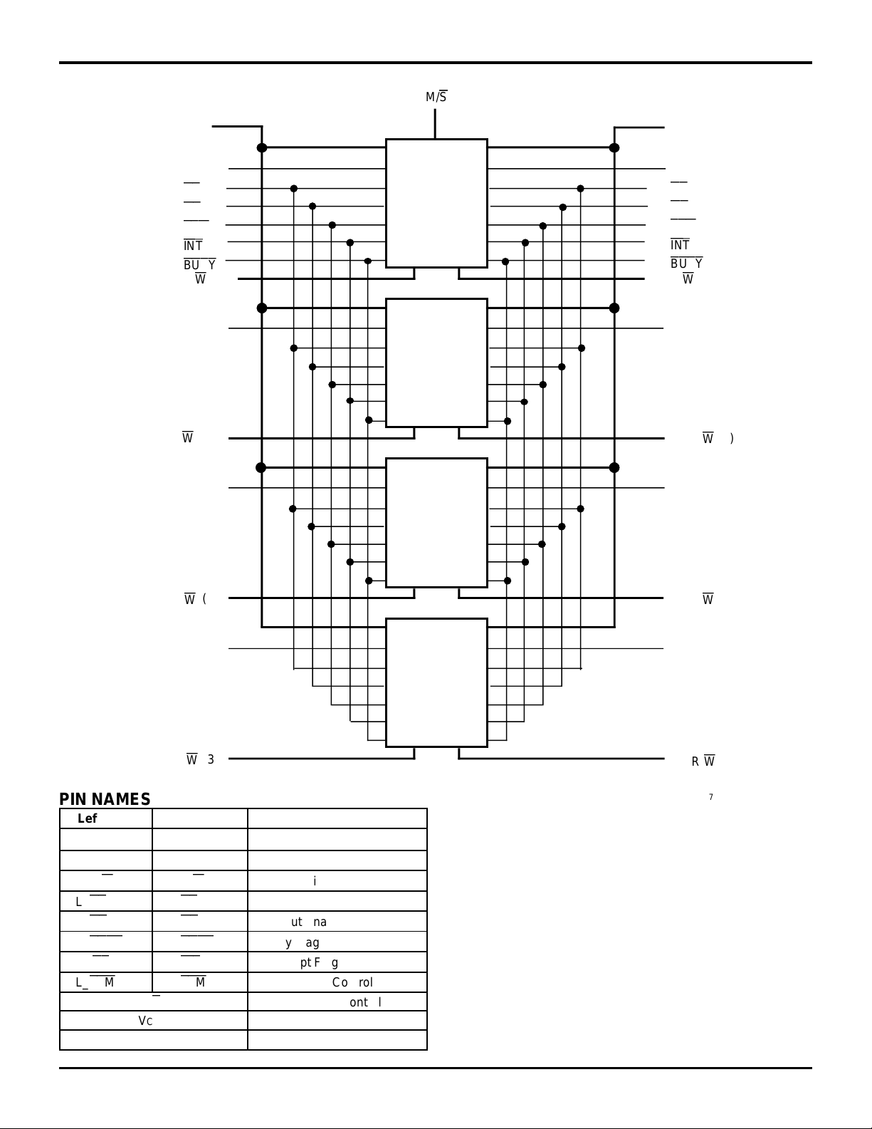
FUNCTIONAL BLOCK DIAGRAM
L_A(0–13)
L_I/O(0–7)
L_
CS
L_
OE
L_
SEM
L_
INT
L_
BUSY
(0)
L_
R/
W
L_I/O(8–15)
R/
(1)
W
L_
L_I/O(16–23)
M/S
IDT7006
16K x 8
(ARBITRATION
LOGIC)
IDT7006
16K x 8
(ARBITRATION
LOGIC)
IDT7006
16K x 8
R_A(0–13)
R_I/O(0–7)
R_
CS
R_
OE
R_
SEM
R_
INT
R_
BUSY
R/
W
(0)
R_
R_I/O(8–15)
R_
R/
R_I/O(16–23)
(1)
W
R/
(2)
W
L_
L_I/O(24–31)
L_ R_
(3)
R/
W
PIN NAMES
Left Port Right Port Description
L_A (0–13) R_A (0–13) Address Inputs
L_I/O (0–31) R_I/O (0–31) Data Inputs/Outputs
L_R/W (1–4) R_R/W (1–4) Read/Write Enables
L_
L_
L_
L_I
L_
CS
OE
BUSY
NT
SEM
R_
M/
CS
R_
OE
R_
BUSY
R_
INT
R_
SEM
S
Chip Select
Output Enable
Busy Flag
Interrupt Flag
Semaphore Control
Master/Slave Control
VCC Power
GND Ground
(ARBITRATION
LOGIC)
IDT7006
16K x 8
(ARBITRATION
LOGIC)
2795 tbl 01
R/
(2)
W
R_
R_I/O(24–31)
(3)
R/
W
2795 drw 02
7.02 2
Page 3
IDT7M1002
16K x 32 CMOS DUAL-PORT STATIC RAM MODULE MILITARY AND COMMERCIAL TEMPERATURE RANGES
ABSOLUTE MAXIMUM RATINGS
(1)
Symbol Rating Commerical Military Unit
TERM Terminal Voltage –0.5 to +7.0 –0.5 to +7.0 V
V
with Respect to
GND
A Operating 0 to +70 –55 to +125 °C
T
Temperature
BIAS Temperature –55 to +125 –65 to +135 °C
T
Under Bias
STG Storage –55 to +125 –65 to +150 °C
T
Temperature
OUT DC Output 50 50 mA
I
Current
NOTE:
Stresses greater than those listed under ABSOLUTE MAXIMUM RATINGS
may cause permanent damage to the device. This is a stress rating only and
functional operation of the device at these or any other conditions above those
indicated in the operational sections of this specification is not implied.
Exposure to absolute maximum rating conditions for extended periods may
affect reliability.
2795 tbl 02
DC ELECTRICAL CHARACTERISTICS
(VCC = 5V ± 10%, TA = –55°C to +125°C or 0°C to +70°C)
RECOMMENDED OPERATING
TEMPERATURE AND SUPPLY VOLTAGE
Ambient
Grade Temperature GND VCC
Military –55°C to +125°C 0V 5.0V ± 10%
Commercial 0°C to +70°C 0V 5.0V ± 10%
2795 tbl 03
RECOMMENDED DC
OPERATING CONDITIONS
Symbol Parameter Min. Typ. Max. Unit
VCC Supply Voltage 4.5 5.0 5.5 V
GND Supply Voltage 0 0 0 V
VIH Input High Voltage 2.2 — 6.0 V
IL Input Low Voltage –0.5
V
NOTE:
1. VIL ≥ –3.0V for pulse width less than 20ns
(1)
— 0.8 V
2795 tbl 04
Symbol Parameter Test Conditions Min. Max. Units
LI| Input Leakage VCC = Max. — 40 µA
|I
(Address & Control) VIN = GND to VCC
|ILI| Input Leakage VCC = Max. — 10 µA
(Data) VIN = GND to VCC
|ILO| Output Leakage VCC = Max. — 10 µA
(Data)
CS
≥ VIH, VOUT = GND to VCC
VOL Output Low VCC = Min. IOL = 4mA — 0.4 V
Voltage
OH Output High VCC = Min, IOH = –4mA 2.4 — V
V
Voltage
DC ELECTRICAL CHARACTERISTICS
(VCC = 5V ± 10%, TA = –55°C to +125°C or 0°C to +70°C)
Commercial Military
Symbol Parameter Test Conditions Min. Max. Min. Max. Units
I
CC2 Dynamic Operating Current VCC = Max.,
(Both Ports Active) Outputs Open, f = fMAX
ISB Standby Supply Current VCC = Max., L_
(Both Ports Inactive) Outputs Open, f = fMAX
ISB1 Standby Suppy Current VCC = Max., L_
(One Port Inactive) Outputs Open, f = fMAX
ISB2 Full Standby Supply Current L_
(Both Ports Inactive) V
CS
IN > VCC – 0.2V or < 0.2V
L_
SEM
CS
≤ VIL,
SEM
= Don’t Care — 1360 — 1600 mA
CS
and R_
CS
≥ VIH — 280 — 340 mA
CS
or R_
CS
≥ VIH — 1000 — 1160 mA
and R_CS ≥ VCC – 0.2V — 60 — 120 mA
and R_
SEM
≥ V
CC – 0.2V
2795 tbl 05
2795 tbl 06
7.02 3
Page 4
IDT7M1002
16K x 32 CMOS DUAL-PORT STATIC RAM MODULE MILITARY AND COMMERCIAL TEMPERATURE RANGES
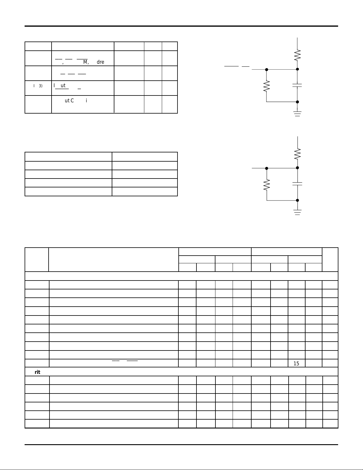
CAPACITANCE
(1)
(TA = +25°C, f = 1.0MHz)
+5V
Symbol Parameter Condition Max. Unit
IN (1) Input Capacitance VIN = 0V 40 pF
C
(CS, OE,
IN(2) Input Capacitance VIN = 0V 12 pF
C
(R/W,
IN(3) Input Capacitance VIN = 0V 45 pF
C
(
BUSY
OUT Output Capacitance VOUT = 0V 12 pF
C
SEM
I/O, INT
, M/S)
, Address)
)
BUSY, INT
255Ω
480Ω
30pF*
(I/O)
*Including scope and jig capacitances.
Figure 1. Output Load
2795 drw 03
NOTE:
1. This parameter is guaranteed by design but not tested.
2795 tbl 07
+5V
AC TEST CONDITIONS
Input Pulse Levels GND to 3.0V
Input Rise/Fall Times 5ns
DATA
OUT
Input Timing Reference Levels 1.5V
Output Reference Levels 1.5V
255Ω
Output Load See Figures 1 and 2
2795 tbl 08
*Including scope and jig capacitances.
Figure 2. Output Load
CHZ, tCLZ, tOHZ, tOLZ, tWHZ, tOW)
AC ELECTRICAL CHARACTERISTICS
(For t
(VCC = 5V ± 10%, TA = –55°C to +125°C or 0°C to +70°C)
7M1002SxxG 7M1002SxxGB
30 –35 –40 –45
Symbol Parameter Min. Max. Min. Max. Min. Max. Min. Max. Unit
Read Cycle
tRC Read Cycle Time 30 — 35 — 40 — 45 — ns
tAA Address Access Time — 30 — 35 — 40 — 45 ns
(2)
tACS
tOE Output Enable Access Time — 17 — 20 — 22 — 25 ns
tOH Output Hold from Address Change 3 — 3 — 3 — 3 — ns
tLZ
tHZ
tPU
tPD
tSOP Sem. Flag Update Pulse (OE or
Write Cycle
tWC Write Cycle Time 30 — 35 — 40 — 45 — ns
tCW
tAW Address Valid to End-of-Write 25 — 30 — 35 — 40 — ns
tAS Address Set-Up Time 0 — 0 — 0 — 0 — ns
tWP Write Pulse Width 25 — 30 — 35 — 35 — ns
tWR Write Recovery Time 0 — 0 — 0 — 0 — ns
Chip Select Access Time — 30 — 35 — 40 — 45 ns
(1)
Output to Low-Z 3 — 3 — 3 — 5 — ns
(1)
Output to High-Z — 15 — 15 — 17 — 20 ns
(1)
Chip Select to Power Up Time 0 — 0 — 0 — 0 — ns
(1)
Chip Deselect to Power Up Time — 50 — 50 — 50 — 50 ns
SEM
) 15 — 15 — 15 — 15 — ns
(2)
Chip Select to End-of-Write 25 — 30 — 35 — 40 — ns
(Continued on next page)
480Ω
5pF*
2795 drw 04
2795 tbl 09
7.02 4
Page 5

IDT7M1002
16K x 32 CMOS DUAL-PORT STATIC RAM MODULE MILITARY AND COMMERCIAL TEMPERATURE RANGES
AC ELECTRICAL CHARACTERISTICS
(VCC = 5V ± 10%, TA = 55°C to +125°C or 0°C to +70°C)
7M1002SxxG 7M1002SxxGB
30 –35 –40 –45
Symbol Parameter Min. Max. Min. Max. Min. Max. Min. Max. Unit
Write Cycle (continued)
DW Data Valid to End-of-Write 22 — 25 — 25 — 25 — ns
t
DH Data Hold Time 0 — 0 — 0 — 0 — ns
t
(1)
t
HZ
OW
t
t
SWRD
SPS
t
Busy Cycle-Master Mode
tBAA
BDA
t
BAC
t
BDC
t
t
WDD
t
DDD Write Data Valid to Read Data Delay — 40 — 45 — 50 — 55 ns
t
APS
t
BDD
Busy Cycle-Slave Mode
tWB
t
WH
WDD
t
Interrupt Timing
AS Address Set-Up Time 0 — 0 — 0 — 0 — ns
t
WR Write Recovery Time 0 — 0 — 0 — 0 — ns
t
INS Interrupt Set Time — 25 — 30 — 32 — 35 ns
t
INR Interrupt Reset Time — 25 — 30 — 32 — 35 ns
t
NOTES:
1. This parameter is guaranteed by design but not tested.
2. To access RAM, CS ≤ V
3. When the module is being used in the Master Mode (M/S ≥ V
4. When the module is being used in the Slave Mode (M/S ≤ V
5. Port-to-Port delay through the RAM cells from the writing port to the reading port.
6. To ensure that the earlier of the two ports wins.
7. To ensure that the write cycle is inhibited during contention.
8. To ensure that a write cycle is completed after contention.
9. tBDD is a calculated parameter and is the greater of 0, tWDD - tWP (actual), or tDDD - tWP (actual).
Output to High-Z — 15 — 15 — 17 — 20 ns
(1)
Output Active from End-of-Write 0 — 0 — 0 — 0 — ns
SEM
Flag Write to Read Time 10 — 10 — 10 — 10 — ns
SEM
Flag Contention Window 10 — 10 — 10 — 10 — ns
BUSY
Access Time to Address — 30 — 35 — 35 — 35 ns
BUSY
Disable Time to Address — 25 — 30 — 30 — 30 ns
BUSY
Access Time to Chip Select — 25 — 30 — 30 — 30 ns
BUSY
Disable Time to Chip Deselect — 25 — 25 — 25 — 25 ns
Write Pulse to Data Delay — 55 — 60 — 65 — 70 ns
Arbitration Priority Set-Up Time 5 — 5 — 5 — 5 — ns
BUSY
Disable to Valid Time — NOTE 9 — NOTE 9 — NOTE 9 — NOTE 9 ns
Write to BUSY Input 0 — 0 — 0 — 0 — ns
Write Hold after BUSY 25 — 25 — 25 — 25 — ns
Write Pulse to Data Delay — 55 — 60 — 65 — 70 ns
(5)
(6)
(7)
(8)
(5)
(4)
IL and
(3)
SEM
≥ VIH. To access semaphore, CS ≥ VIH and
IH).
IL).
SEM
2795 tbl 10
≤ VIL.
7.02 5
Page 6

IDT7M1002
OE
CS
16K x 32 CMOS DUAL-PORT STATIC RAM MODULE MILITARY AND COMMERCIAL TEMPERATURE RANGES
TIMING WAVEFORM OF READ CYCLE NO. 1, EITHER SIDE
t
RC
ADDRESS
t
AA
DATA
OUT
PREVIOUS
DATA VALID
t
OH
DATA VALID
TIMING WAVEFORM OF READ CYCLE NO. 2, EITHER SIDE
t
SOP
t
SOP
t
ACE
t
AOE
(1, 2, 4)
(1, 3, 5)
t
OH
2795 drw 05
(6)
t
CHZ
DATA
OUT
(6)
t
OLZ
DATA VALID
(6)
t
I
CC
CLZ
t
OHZ
(6)
(6)
t
PD
CURRENT 50% 50%
I
SB
NOTES:
1. R/W is HIGH for Read Cycles
2. Device is continuously enabled CS ≤ V
3. Addresses valid prior to or coincident with CS transition LOW.
4.OE ≤ V
5. To access RAM, CS ≤ VIL and
6. This parameter is guaranteed by design but not tested.
IL
SEM
(6)
t
PU
IL. This waveform cannot be used for semaphore reads.
≥ VIH. To access semaphore, CS ≥ VIH and
SEM
≤ VIL.
2795 drw 06
7.02 6
Page 7

IDT7M1002
CS
OE
W
W
CS
16K x 32 CMOS DUAL-PORT STATIC RAM MODULE MILITARY AND COMMERCIAL TEMPERATURE RANGES
TIMING WAVEFORM OF WRITE CYCLE NO. 1 (R/
WC
t
ADDRESS
tAW
R/
DATAOUT
DATAIN
(6)
tAS
(4) (4)
tWHZ
tWP
(2)
(9)
WW
W
CONTROLLED TIMING)
WW
OW
t
tDW
tDH
DATA VALID
(9)
tWR
(1, 2, 4)
(7)
tCHZ
(9)
2795 drw 07
TIMING WAVEFORM OF WRITE CYCLE NO. 2 (
WC
t
CSCS
CS
CONTROLLED TIMING)
CSCS
(1, 2, 4)
ADDRESS
t
AW
(6)
t
AS
t
WP
(2)
t
WR
(7)
R/
t
DW
DATA
IN
NOTES:
1. R/W must be HIGH during all address transitions.
2. A write occurs during the overlap (t
WR is measured from the earlier of
3. t
4. During this period, the I/O pins are in the output state and input signals must be applied.
5. If the CS or
6. Timing depends on which enable signal is asserted last.
7. Timing depends on which enable signal is de-asserted first.
8. If OE is LOW during a R/W controlled write cycle, the write pulse width must be the larger of tWP or (tWZ + tDW) to allow the I/O drivers to
turn off and data to be placed on the bus for the required t
not apply and the write pulse can be as short as the specified t
SEM
low transition occurs simultaneously with or after the R/W low transition, the outputs remain in the high impedance state.
WP) of a LOW
CS
or R/W (or
CS
and a LOW R/W.
SEM
or R/W) going HIGH to the end of write cycle.
DW. If
OE
is HIGH during an R/W controlled write cycle, this requirement does
WP.
DATA VALID
t
DH
2795 drw 08
7.02 7
Page 8

IDT7M1002
W
SEM
D
OE
"
SEM
"
WBSEM
W
16K x 32 CMOS DUAL-PORT STATIC RAM MODULE MILITARY AND COMMERCIAL TEMPERATURE RANGES
TIMING WAVEFORM OF SEMAPHORE READ AFTER WRITE, EITHER SIDE
t
A0–A
2
DATA
0
R/
NOTE:
1.CS ≥ V
AW
t
WP
t
DW
DATA
IN
VALI
t
t
AS
IH for the duration of the above timing (both write and read cycle).
WP
t
DH
t
WR
t
SWRD
t
SOP
t
SOP
t
AA
VALID ADDRESSVALID ADDRESS
t
ACE
t
AOE
READ CYCLEWRITE CYCLE
(1)
DATA
VALID
OUT
2795 drw 09
t
OH
TIMING WAVEFORM OF SEMAPHORE CONTENTION
A
0A
— A
2A
(2)
SIDE "A
(2)
SIDE "B
NOTES:
1. D
OR = DOL ≤ VIL, (L_
2. “A” may be either left or right port. “B” is the opposite port from “A”.
3. This parameter is measured from R/
4. If tSPS is violated, the semaphore will fall positively to one side or the other, but there is no guarantee which side will obtain the flag.
R/
A
A
A
0B
— A
2B
R/
B
CS
= R_ CS) ≥ VIH Semaphore Flag is released from both sides (reads as ones from both sides) at cycle start.
A or
SEM
W
A going HIGH to R/WB or
MATCH
t
SPS
MATCH
SEM
(1, 3, 4)
B going HIGH.
2795 drw 10
7.02 8
Page 9

IDT7M1002
BUSY
W
W
16K x 32 CMOS DUAL-PORT STATIC RAM MODULE MILITARY AND COMMERCIAL TEMPERATURE RANGES
TIMING WAVEFORM OF READ WITH
ADDR
R
R/
R
DATA
IN R
(1)
t
APS
ADDR
L
L
DATA
OUT L
NOTES:
1. To ensure that the earlier of the two ports wins.
2. (L_ CS = R_ CS) ≤ V
3.OE ≤ VIL for the reading port.
IL
BUSYBUSY
BUSY
BUSYBUSY
t
MATCH
WC
(M/
S S
S
≥ VIH)
S S
t
WP
(2)
t
DW
VALID
MATCH
t
WDD
t
DDD
(3)
t
BDA
t
BDD
t
DH
VALID
2795 drw 11
TIMING WAVEFORM OF WRITE WITH PORT-TO-PORT DELAY (M/
tWC
ADDR R
R/
R
DATAIN R
ADDR L
DATA
OUT L
NOTES:
1.
BUSY
2. (L_ CS = R_ CS) ≤ V
input equals HIGH for the writing port.
IL
MATCH
tWP
tDW tDH
VALID
MATCH
tWDD
SS
S
≤ VIH)
SS
tDDD
(1, 2)
VALID
2795 drw 12
7.02 9
Page 10

IDT7M1002
BUSY
W
CS
CS
BUSY
BUSY
16K x 32 CMOS DUAL-PORT STATIC RAM MODULE MILITARY AND COMMERCIAL TEMPERATURE RANGES
TIMING WAVEFORM OF WRITE WITH
R/
t
WB
BUSYBUSY
BUSY
BUSYBUSY
DATA
INPUT (M/
INR
TIMING WAVEFORM OF BUSY ARBITRATION (
ADDR "A"
AND "B"
"A"
"B"
(2)
APS
t
ADDRESS MATCH
SS
S
≤ VIL)
SS
t
WP
t
WH
CSCS
CS
CONTROLLED TIMING)
CSCS
t
BDC
2795 drw 13
(1)
t
BAC
"B"
2795 drw 14
TIMING WAVEFORM OF BUSY ARBITRATION (CONTROLLED BY ADDRESS MATCH TIMING
ADDR "A"
(2)
t
APS
ADDR"B"
"B"
NOTES:
1. All timing is the same for the left and right ports. Port “A” may be either the left or right port. Port “B” is the port opposite from “A”.
APS is violated, the busy signal will be asserted on one side or another but there is no guarantee on which side busy will be asserted.
2. If t
ADDRESS "N"
MATCHING ADDRESS "N"
t
BAA
t
BDA
2795 drw 15
(1)
7.02 10
Page 11

IDT7M1002
CE
INT
W
CE
OE
INT
16K x 32 CMOS DUAL-PORT STATIC RAM MODULE MILITARY AND COMMERCIAL TEMPERATURE RANGES
TIMING WAVEFORM OF INTERRUPT CYCLE
ADDR "A"
"A"
R/
1"A"
"B"
ADDR "B"
"B"
(3)
t
AS
(3)
t
AS
INTERRUPT SET ADDRESS
(3)
t
INS
INTERRUPT CLEAR ADDRESS
(1)
t
WC
t
RC
(2)
(2)
t
WR
(4)
2795 drw 16
"B"
(3)
t
INR
"B"
NOTES:
1. All timing is the same for left and right ports. Port “A” may be either the left or right port. Port “B” is the port opposite from “A”.
2. See Interrupt truth table.
3. Timing depends on which enable signal is asserted last.
4. Timing depends on which enable signal is de-asserted first.
TRUTH TABLE I: Non-Contention Read/Write Control
(1)
Inputs Outputs Mode
CSCS
CS
CSCS
R/W
OEOE
OE
OEOE
SEMSEM
SEM
SEMSEM
I/O Description
H X X H High-Z Deselected or Power Down
L L X H Data_In Write
L H L H Data_OUT Read
X X H X High-Z Outputs Disabled
NOTE:
1. The conditions for non-contention are L_A (0–13) ≠ R_A (0–13).
2. denotes a LOW to HIGH waveform transition.
TRUTH TABLE II: Semaphore Read/Write Control
(2)
Inputs
CSCS
CS
CSCS
R/
WW
W
WW
OEOE
OE
OEOE
SEMSEM
SEM
SEMSEM
H H L L Data_OUT Read Data in Semaphore Flag
H X L Data_IN Write Data_IN (0, 8, 16, 24)
L X X L — Not Allowed
Outputs Mode
I/O Description
2795 drw 17
2795 tbl 13
2795 tbl 14
7.02 11
Page 12

IDT7M1002
16K x 32 CMOS DUAL-PORT STATIC RAM MODULE MILITARY AND COMMERCIAL TEMPERATURE RANGES
INTERRUPT/BUSY FLAGS, DEPTH & WIDTH EXPANSION, MASTER/SLAVE CONTROL,
SEMAPHORES
For more details regarding Interrupt/Busy flags, depth and/or width expansion, master/slave control, or semaphore
operations, please consult the IDT7006 data sheet.
PACKAGE DIMENSIONS
0.125
1.325
1.355
0.025
0.060
0.200
0.100
BSC
TOP VIEW
1.200
BSC
1.200
BOTTOM VIEW
Pin A1
ORDERING INFORMATION
IDT XXXX A 999 A A
Device Power Speed Package Process/
Type Temperature
Range
1.325
1.355
BSC
0.235
MAX.
0.016
0.020
0.040
0.060
0.175
MAX.
2795 drw 18
BLANK Commercial (0°C to +70°C)
B Military (–55°C to +125°C)Semiconductor
Components compliant to MIL-STD-883, Class B
G Ceramic PGA (Pin Grid Array)
30
35
40
45
S Standard Power
7M1002 16K x 32 CMOS Dual-Port Static RAM Module
7.02 12
(Commercial Only)
(Commercial Only)
(Military Only)
(Military Only)
Speed in Nanoseconds
2795 drw 19
 Loading...