

Datasheet IDT79R3052E20J, IDT79R305240MJ, IDT79R305240J, IDT79R305233MJ, IDT79R305233J Datasheet (Integrated Device Technology)
...Page 1
COMMERCIAL TEMPERATURE RANGE SEPTEMBER 1995
1995 Integrated Device Technology, Inc. 5.3 DSC-3000/5
IDT79R3051/79R3052
RISControllers
IDT79R3051, 79R3051E
IDT79R3052
, 79R3052E
FEATURES:
• Instruction set compatible with IDT79R3000A and
IDT79R3001 MIPS RISC CPUs
• High level of integration minimizes system cost, power
consumption
— IDT79R3000A /IDT79R3001 RISC Integer CPU
— R3051 features 4KB of Instruction Cache
— R3052 features 8KB of Instruction Cache
— All devices feature 2kB of Data Cache
— “E” Versions (Extended Architecture) feature full
function Memory Management Unit, including 64-
entry Translation Lookaside Buffer (TLB)
— 4-deep write buffer eliminates memory write stalls
— 4-deep read buffer supports burst refill from slow
memory devices
— On-chip DMA arbiter
— Bus Interface minimizes design complexity
• Single clock input with 40%-60% duty cycle
• 35 MIPS, over 64,000 Dhrystones at 40MHz
• Low-cost 84-pin PLCC packaging that's pin-/packagecompatible with thermally enhanced 84-pin MQUAD.
• Flexible bus interface allows simple, low-cost designs
• 20, 25, 33, and 40MHz operation
• Complete software support
— Optimizing compilers
— Real-time operating systems
— Monitors/debuggers
— Floating Point Software
— Page Description Languages
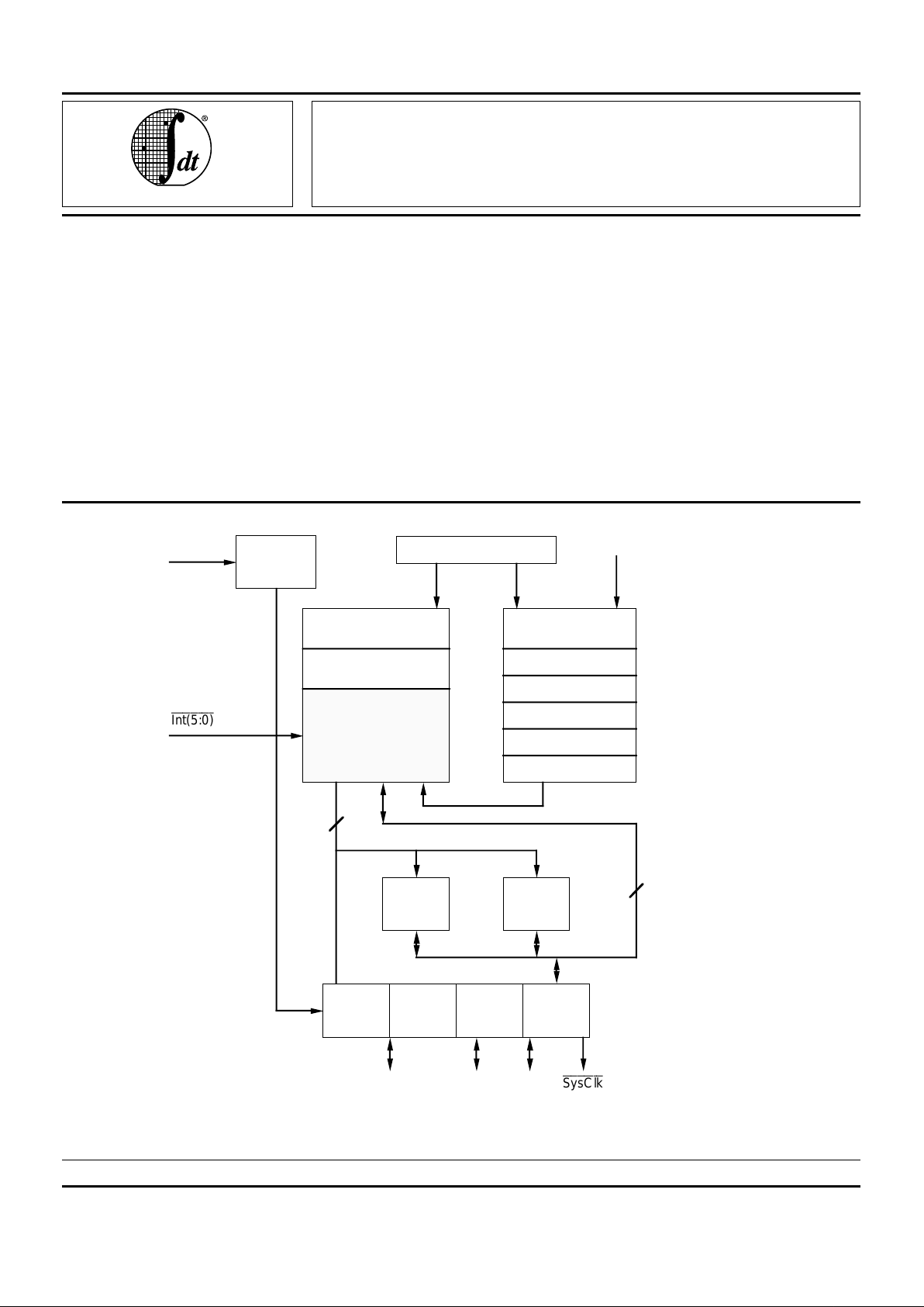
1
Clock
Generator
Unit
Master Pipeline Control
System Control
Coprocessor
Integer
CPU Core
Exception/Control
Registers
Memory Management
Registers
Translation
Lookaside Buffer
(64 entries)
General Registers
(32 x 32)
ALU
Shifter
Mult/Div Unit
Address Adder
PC Control
Virtual Address
Data
Cache
(2kB)
Instruction
Cache
(8kB/4kB)
Physical Address Bus
BIU
Control
DMA
Arbiter
4-deep
Read
Buffer
4-deep
Write
Buffer
Clk2xIn
Int(5:0)
32
32
BrCond(3:0)
Data Bus
Bus Interface Unit
Address/
Data
DMA
Ctrl
Rd/Wr
Ctrl
SysClk
2874 drw 01
The IDT logo is a registered trademark, and RISChipset, RISController, R3041, R3051, R3052, R3071, R3081, R3720, R4400 and R4600 are trademarks of Integrated Device Technology, Inc.
Figure 1. R3051 Family Block Diagram
Integrated Device Technology, Inc.
Page 2

5.3 2
IDT79R3051/79R3052 INTEGRATED RISControllers COMMERCIAL TEMPERATURE RANGE
INTRODUCTION
The IDT IDT79R3051 family is a series of high-performance 32-bit microprocessors featuring a high level of integration which are targeted to high-performance, but costsensitive embedded processing applications. The IDT79R3051
family is designed to bring the high-performance inherent in
the MIPS RISC architecture into low-cost, simplified, powersensitive applications.
Functional units were integrated onto the CPU core in order
to reduce the total system cost, without significantly degrading
system performance. Thus, the IDT79R3051 family is able to
offer 35MIPS of integer performance at 40MHz without requiring external SRAM or caches.
Furthermore, the IDT79R3051 family brings dramatic power
reduction to these embedded applications, allowing the use of
low-cost packaging for devices up to 25 MHz. The IDT79R3051
family allows customer applications to bring maximum performance at minimum cost.
Figure 1 shows a block-level representation of the functional units within the IDT79R3051 family. The IDT79R3051
family could be viewed as the embodiment of a discrete
solution built around the IDT79R3000A or IDT79R3001.
However, by integrating this functionality on a single chip,
dramatic cost and power reductions are achieved.
Currently, there are four members of the IDT79R3051
family. All devices are pin- and software-compatible: the
differences lie in the amount of instruction cache, and in the
memory management capabilities of the processor:
• The IDT79R3052"E” incorporates 8kB of Instruction Cache,
and features a full-function Memory Management Unit
(MMU), including a 64-entry fully-associative Translation
Lookaside Buffer (TLB). This is the same MMU incorporated
into the IDT79R3000A and IDT79R3001.
• The IDT79R3052 also incorporates 8kB of Instruction Cache.
However, the MMU is a much simpler subset of the capabilities of the enhanced versions of the architecture, and in fact
does not use a TLB.
• The IDT79R3051"E” incorporates 4KB of Instruction Cache.
Additionally, this device features the same full-function
MMU (including TLB file) as the IDT79R3052"E”, and
IDT79R3000A.
• The IDT79R3051 incorporates 4KB of Instruction Cache,
and uses the simpler memory management model of the
IDT79R3052.
An overview of the functional blocks incorporated in these
devices follows.
CPU Core
The CPU core is a full 32-bit RISC integer execution
engine, capable of sustaining close-to single cycle execution
rate. The CPU core contains a five stage pipeline and 32
orthogonal 32-bit registers. The IDT79R3051 family implements the MIPS ISA. In fact, the execution engine of the
IDT79R3051 family is the same as the execution engine of the
IDT79R3000A (and IDT79R3001). Thus the IDT79R3051
family is binary-compatible with those CPU engines.
Figure 2. R3051 Family 5-Stage Pipeline
The execution engine of the IDT79R3051 family uses a
five-stage pipeline to achieve close-to single cycle execution.
A new instruction can be started in every clock cycle; the
execution engine actually processes five instructions concurrently (in various pipeline stages). Figure 2 shows the
concurrency achieved by the IDT79R3051 family pipeline.
IF
Current
CPU
Cycle
I#1 ALURD MEM WB
IFI#2 ALURD MEM WB
IFI#3 ALURD MEM WB
IFI#4 ALURD MEM WB
IFI#5 ALURD MEM WB
2874 drw 02
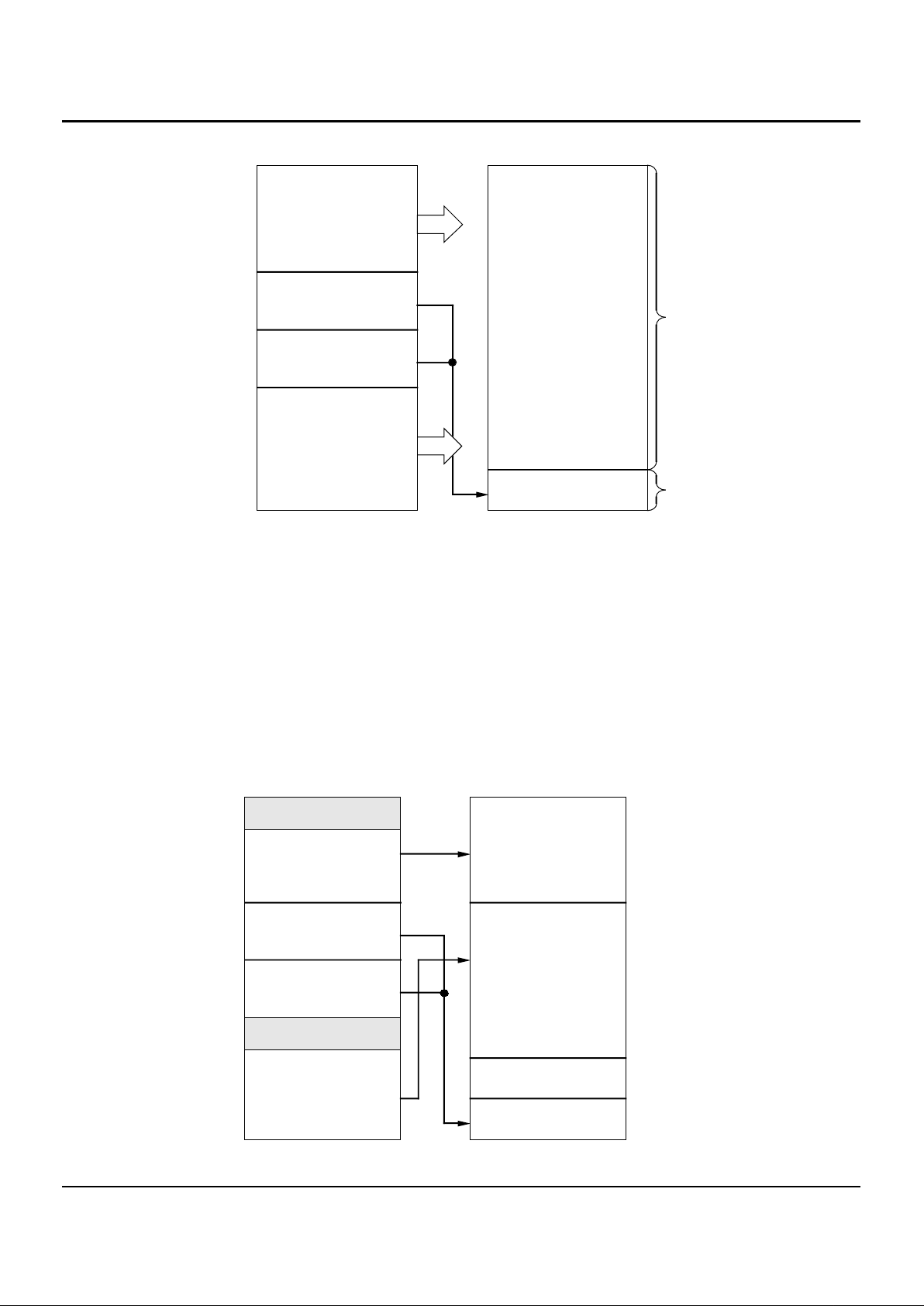
System Control Co-Processor
The R3051 family also integrates on-chip the System
Control Co-processor, CP0. CP0 manages both the exception handling capability of the IDT79R3051 family, as well as
the virtual to physical mapping of the IDT79R3051 family.
There are two versions of the IDT79R3051 family architecture: the Extended Architecture Versions (the IDT79R3051E
and IDT79R3052E) contain a fully associative 64-entry TLB
which maps 4KB virtual pages into the physical address
space. The virtual to physical mapping thus includes kernel
segments which are hard mapped to physical addresses, and
kernel and user segments which are mapped on a page basis
by the TLB into anywhere within the 4GB physical address
space. In this TLB, 8-page translations can be “locked” by the
kernel to insure deterministic response in real-time applications. These versions thus use the same MMU structure as
that found in the IDT79R3000A and IDT79R3001. Figure 3
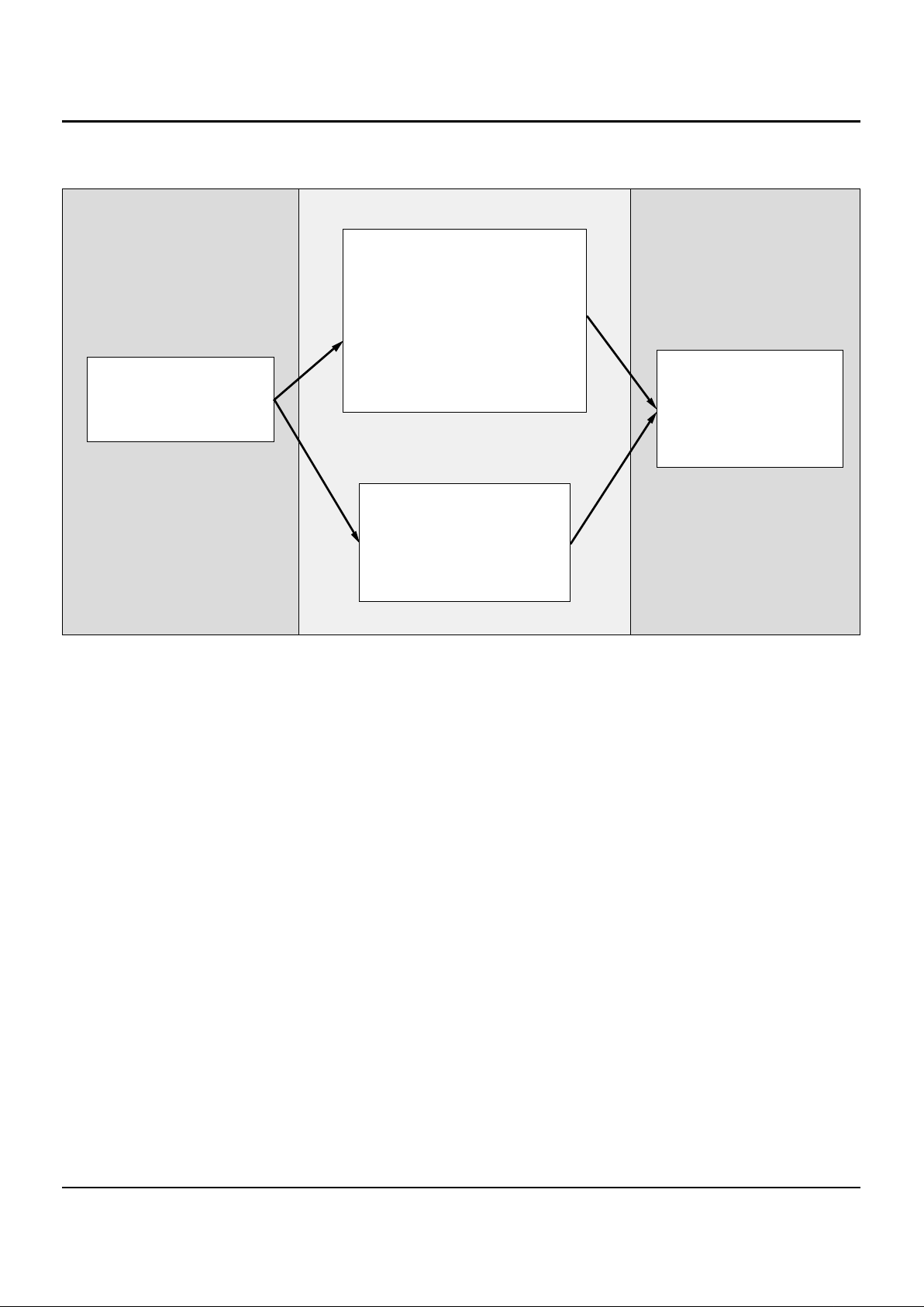
shows the virtual-to-physical address mapping found in the
Extended Architecture versions of the processor family.
The Extended Architecture devices allow the system
designer to implement kernel software to dynamically manage
User task utilization of memory resources, and also allow the
Kernel to effectively “protect” certain resources from user
tasks. These capabilities are important in a number of
embedded applications, from process control (where resource
protection may be extremely important) to X-Window display
systems (where virtual memory management is extremely
important), and can also be used to simplify system debugging.
Page 3
5.3 3
IDT79R3051/79R3052 INTEGRATED RISControllers COMMERCIAL TEMPERATURE RANGE
Figure 3. Virtual-to-Physical Mapping of Extended Architecture Versions
Kernel Mapped
(kseg2)
Kernel Uncached
(kseg1)
Kernel Cached
(kseg0)
User Mapped
Cacheable
(kuseg)
Physical
Memory
Memory
0xffffffff
0xc0000000
0xa0000000
0x80000000
0x00000000
3548MB
512MB
Any
Any
VIRTUAL PHYSICAL
2874 drw 03
Figure 4. Virtual-to-Physical Mapping of Base Architecture Versions
1MB Kernel Rsvd
Kernel Cacheable
Tasks
Kernel/User
Cacheable
Tasks
Inaccessible
Kernel Boot
and I/O
0xffffffff
0xc0000000
0xa0000000
0x80000000
0x00000000
1024MB
2048MB
512MB
512MB
VIRTUAL PHYSICAL
Kernel Cached
(kseg2)
Kernel Uncached
(kseg1)
Kernel Cached
(kseg0)
User
Cached
(kuseg)
1MB User Rsvd
2874 drw 04
The base versions of the architecture (the IDT79R3051
and IDT79R3052) remove the TLB and institute a fixed
address mapping for the various segments of the virtual
address space. The base processors support distinct kernel
and user mode operation without requiring page management
software, leading to a simpler software model. The memory
mapping used by these devices is illustrated in Figure 4. Note
that the reserved address spaces shown are for compatibility
with future family members; in the current family members,
references to these addresses are translated in the same
fashion as their respective segments, with no traps or exceptions taken.
When using the base versions of the architecture, the
system designer can implement a distinction between the
user tasks and the kernel tasks, without having to execute
page management software. This distinction can take the
form of physical memory protection, accomplished by address decoding, or in other forms. In systems which do not
wish to implement memory protection, and wish to have the
kernel and user tasks operate out of a single unified memory
space, upper address lines can be ignored by the address
decoder, and thus all references will be seen in the lower
gigabyte of the physical address space.
Page 4

5.3 4
IDT79R3051/79R3052 INTEGRATED RISControllers COMMERCIAL TEMPERATURE RANGE
Clock Generation Unit
The IDT79R3051 family is driven from a single input clock,
capable of operating in a range of 40%-60% duty cycle. On
chip, the clock generator unit is responsible for managing the
interaction of the CPU core, caches, and bus interface. The
clock generator unit replaces the external delay line required
in IDT79R3000A and IDT79R3001 based applications.
Instruction Cache
The current family includes two different instruction cache
sizes: the IDT79R3051 family (the IDT79R3051 and
IDT79R3051E) feature 4KB of instruction cache, and the
IDT79R3052 and IDT79R3052E each incorporate 8KB of
Instruction Cache. For all four devices, the instruction cache
is organized as a line size of 16 bytes (four words). This
relatively large cache achieves a hit rate well in excess of 95%
in most applications, and substantially contributes to the
performance inherent in the IDT79R3051 family. The cache is
implemented as a direct mapped cache, and is capable of
caching instructions from anywhere within the 4GB physical
address space. The cache is implemented using physical
addresses (rather than virtual addresses), and thus does not
require flushing on context switch.
Data Cache
All four devices incorporate an on-chip data cache of 2KB,
organized as a line size of 4 bytes (one word). This relatively
large data cache achieves hit rates well in excess of 90% in
most applications, and contributes substantially to the performance inherent in the IDT79R3051 family. As with the instruction cache, the data cache is implemented as a direct mapped
physical address cache. The cache is capable of mapping any
word within the 4GB physical address space.
The data cache is implemented as a write through cache,
to insure that main memory is always consistent with the
internal cache. In order to minimize processor stalls due to
data write operations, the bus interface unit incorporates a 4deep write buffer which captures address and data at the
processor execution rate, allowing it to be retired to main
memory at a much slower rate without impacting system
performance.
Bus Interface Unit
The IDT79R3051 family uses its large internal caches to
provide the majority of the bandwidth requirements of the
execution engine, and thus can utilize a simple bus interface
connected to slow memory devices.
The IDT79R3051 family bus interface utilizes a 32-bit
address and data bus multiplexed onto a single set of pins.
The bus interface unit also provides an ALE signal to demultiplex the A/D bus, and simple handshake signals to
process processor read and write requests. In addition to the
read and write interface, the IDT79R3051 family incorporates
a DMA arbiter, to allow an external master to control the
external bus.
The IDT79R3051 family incorporates a 4-deep write buffer
to decouple the speed of the execution engine from the speed
of the memory system. The write buffers capture and FIFO
processor address and data information in store operations,
and presents it to the bus interface as write transactions at the
rate the memory system can accommodate.
The IDT79R3051/52 read interface performs both single
word reads and quad word reads. Single word reads work with
a simple handshake, and quad word reads can either utilize
the simple handshake (in lower performance, simple systems) or utilize a tighter timing mode when the memory system
can burst data at the processor clock rate. Thus, the system
designer can choose to utilize page or nibble mode DRAMs
(and possibly use interleaving), if desired, in high-performance systems, or use simpler techniques to reduce complexity.
In order to accommodate slower quad-word reads, the
IDT79R3051 family incorporates a 4-deep read buffer FIFO,
so that the external interface can queue up data within the
processor before releasing it to perform a burst fill of the
internal caches. Depending on the cost vs. performance
tradeoffs appropriate to a given application, the system design
engineer could include true burst support from the DRAM to
provide for high-performance cache miss processing, or utilize the read buffer to process quad word reads from slower
memory systems.
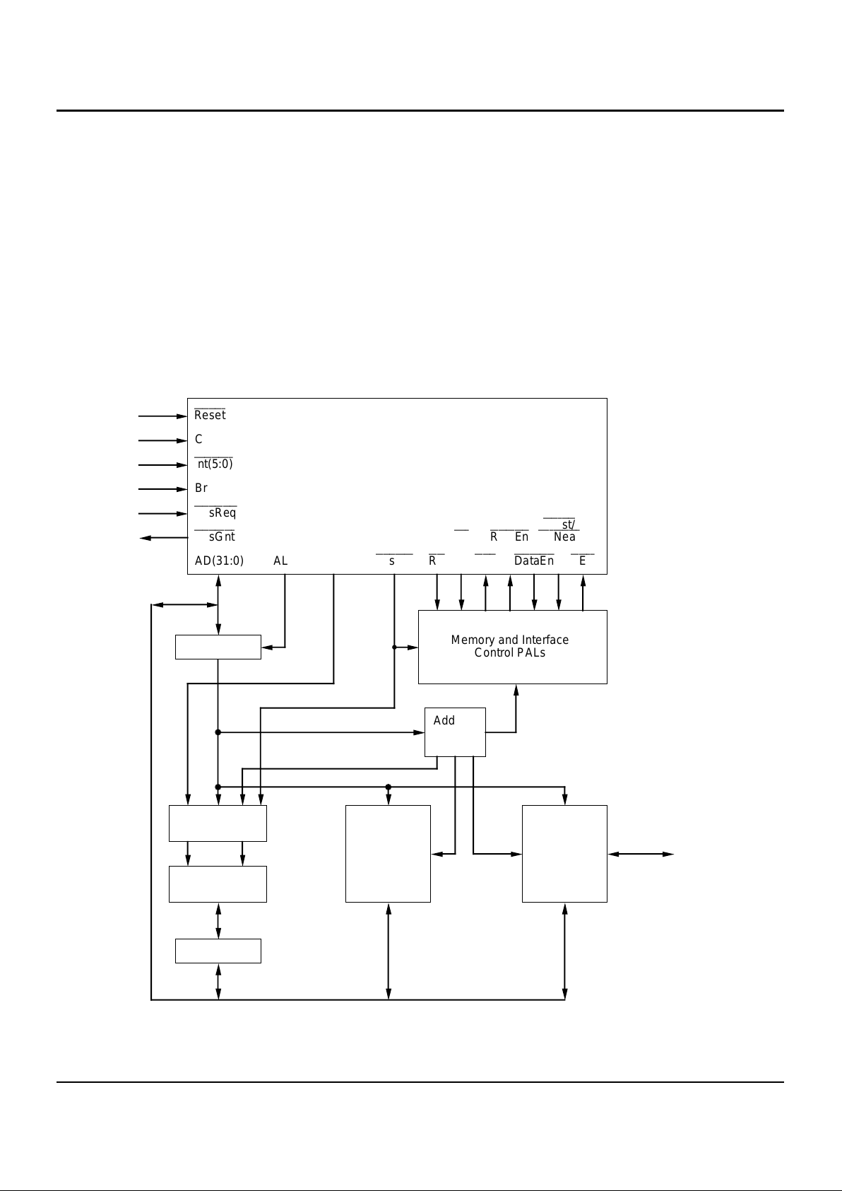
SYSTEM USAGE
The IDT79R3051 family has been specifically designed to
easily connect to low-cost memory systems. Typical low-cost
memory systems utilize slow EPROMs, DRAMs, and application-specific peripherals. These systems may also typically
contain large, slow Static RAMs, although the IDT79R3051
family has been designed to not specifically require the use of
external SRAMs.
Figure 5 shows a typical system block diagram. Transparent latches are used to de-multiplex the IDT79R3051/52
address and data busses from the A/D bus. The data paths
between the memory system elements and the R3051 family
A/D bus is managed by simple octal devices. A small set of
simple PALs can be used to control the various data path
elements, and to control the handshake between the memory
devices and the CPU.
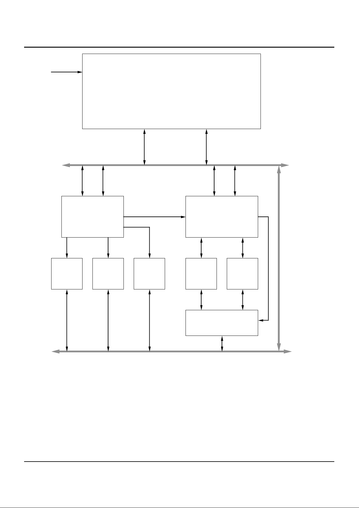
DEVELOPMENT SUPPORT
The IDT79R3051 family is supported by a rich set of
development tools, ranging from system simulation tools
through prom monitor support, logic analysis tools, and subsystem modules.
Figure 7 is an overview of the system development process
typically used when developing IDT79R3051 family-based
applications. The IDT79R3051 family is supported by powerful tools through all phases of project development. These
tools allow timely, parallel development of hardware and
software for IDT79R3051/52 based applications, and include
tools such as:
• A program, Cache-3051, which allows the performance of
an IDT79R3051 family based system to be modeled and
understood without requiring actual hardware.
Page 5
5.3 5
IDT79R3051/79R3052 INTEGRATED RISControllers COMMERCIAL TEMPERATURE RANGE
• Sable, an instruction set simulator.
• Optimizing compilers from MIPS, the acknowledged leader
in optimizing compiler technology.
• IDT Cross development tools, available in a variety of
development environments.
• The high-performance IDT floating point library software,
which has been integrated into the compiler toolchain to
allow software floating point to replace hardware floating
point without modifying the original source code.
• The IDT Evaluation Board, which includes RAM, EPROM,
I/O, and the IDT Prom Monitor.
• The IDT Laser Printer System board, which directly drives
a low-cost print engine, and runs Microsoft TrueImage
Page Description Language on top of PeerlessPage Advanced Printer Controller BIOS.
• Adobe PostScript
Page Description Language, ported to
the R3000 instruction set, runs on the IDT79R3051 family.
• The IDT Prom Monitor, which implements a full prom
monitor (diagnostics, remote debug support, peek/poke,
etc.).
• An In-Circuit Emulator, developed and sold by Embedded
Performance, Inc.
Figure 5. Typical R3051 Family Based System
Reset
Clk2xIn
Int(5:0)
BrCond(3:0)
BusReq
BusGnt
AD(31:0) ALE Addr(3:2)
SysClk Rd
Wr
Ack
RdCEn
DataEn
Burst/
WrNear
BErr
Memory and Interface
Control PALs
Address
Decode
PAL
FCT373T
DRAM Control
PALs
DRAM
FCT245T
EPROM
I/O Devices/
Peripherals
System I/O
IDT R3051 Family
RISController
2874 drw 05
Page 6
5.3 6
IDT79R3051/79R3052 INTEGRATED RISControllers COMMERCIAL TEMPERATURE RANGE
Figure 6. R3051 Family Chip Set Based System
Clk2xIn
IDT79R3051 Family
RISController
Address/
Data
Control
I/O Controller
DRAM
Controller
DRAM DRAMPROM I/O I/O
IDT73720
Bus Exchanger
R3051 Family
Local Bus
(2)
2874 drw 06
Page 7
5.3 7
IDT79R3051/79R3052 INTEGRATED RISControllers COMMERCIAL TEMPERATURE RANGE
Figure 7. R3051 Family Development Toolchain
Cache-R305x
Benchmarks
Evaluation Board
Laser Printer System
SABLE Simulator
DBG Debugger
PIXIE Profiler
MIPS Compiler Suite
Stand-Alone Libraries
Floating Point Library
Cross Development Tools
Adobe PostScript
PDL
MicroSoft TrueImage
PDL
Ada
Cache-R305x
Hardware Models
General CAD Tools
RISC Sub-systems
Evaluation Board
Laser Printer System
Hardware
Software
Logic Analysis
Diagnostics
IDT PROM Monitor
Remote Debug
Real-Time OS
In-Circuit Emulator
System
Architecture
Evaluation
System
Development
Phase
System
Integration
and Verification
2874 drw 07
Page 8

5.3 8
IDT79R3051/79R3052 INTEGRATED RISControllers COMMERCIAL TEMPERATURE RANGE
Airflow (ft/min)
ØCA 0 200 400 600 800 1000
"J" Package 29 26 21 18 16 15
"MJ" Package* 22 14 12 11 9 8
2874 tbl 01
PERFORMANCE OVERVIEW
The IDT79R3051 family achieves a very high level of
performance. This performance is based on:
• An efficient execution engine. The CPU performs ALU
operations and store operations at a single cycle rate, and
has an effective load time of 1.3 cycles, and a branch
execution rate of 1.5 cycles (based on the ability of the
compilers to avoid software interlocks). Thus, the execution
engine achieves over 35MIPS performance when operating
out of cache.
• Large on-chip caches. The IDT79R3051 family contains
caches which are substantially larger than those on the
majority of today’s embedded microprocessors. These large
caches minimize the number of bus transactions required,
and allow the R3051 family to achieve actual sustained
performance, very close to its peak execution rate.
• Autonomous multiply and divide operations. The
IDT79R3051 family features an on-chip integer multiplier/
divide unit which is separate from the other ALU. This allows
the IDT79R3051 family to perform multiply or divide operations in parallel with other integer operations, using a single
multiply or divide instruction rather than “step” operations.
• Integrated write buffer. The IDT79R3051 family features a
four-deep write buffer, which captures store target addresses and data at the processor execution rate and retires
it to main memory at the slower main memory access rate.
Use of on-chip write buffers eliminates the need for the
processor to stall when performing store operations.
• Burst read support. The IDT79R3051 family enables the
system designer to utilize page mode or nibble mode RAMs
when performing read operations to minimize the main
memory read penalty and increase the effective cache hit
rates.
These techniques combine to allow the processor to achieve
35MIPS integer performance, and over 64,000 dhrystones at
40MHz without the use of external caches or zero wait-state
memory devices.
SELECTABLE FEATURES
The IDT79R3051 family allows the system designer to
configure some aspects of operation. These aspects are
established when the device is reset and include:
• Big Endian vs. Little Endian operation: The part can be
configured to operate with either byte ordering convention,
and in fact may also be dynamically switched between the
two conventions. This facilitates the porting of applications
from other processor architectures, and also permits intercommunications between various types of processors and
databases.
• Data cache refill of one or four words: The memory
system must be capable of performing 4-word transfers to
satisfy cache misses. This option allows the system designer to choose between one- and four-word refill on data
cache misses, depending on the performance each option
brings to his application.
THERMAL CONSIDERATIONS
The IDT79R3051 family utilizes special packaging techniques to improve the thermal properties of high-speed processors. Thus, all versions of the IDT79R3051 family are
packaged in cavity-down packaging.
The lowest cost members of the family use a standard
cavity-down, injection molded PLCC package (the "J" package). This package, coupled with the power reduction techniques employed in the design of the IDT79R3051 family,
allows operation at speeds to 25MHz. However, at higher
speeds, additional thermal care must be taken.
For this reason, the IDT79R3051 family is also available in
the MQUAD package (the "MJ" package), which is an allaluminum package with the die attached to a normal copper
lead-frame, mounted to the aluminum casing. The MQUAD
allows for more efficient thermal transfer between the die and
the case of the part due to the heat-spreading effect of the
aluminum. The aluminum offers less internal resistance from
one end of the package to the other, which reduces the
temperature gradient across the package, and, therefore,
presents a greater area for convection and conduction to the
PCB for a given temperature. Even nominal amounts of
airflow will dramatically reduce the junction temperature of the
die, resulting in cooler operation. The MQUAD package is
available at all frequencies, and is pin- and form-compatible
with the PLCC package. Thus, designers can choose to utilize
this package without changing their PCB.
The members of the IDT79R3051 family are guaranteed in
a case temperature range of 0°C to +85°C. The type of
package, speed (power) of the device, and airflow conditions
affect the equivalent ambient conditions which meet this
specification.
The equivalent allowable ambient temperature, T
A, can be
calculated using the thermal resistance from case to ambient
(ØCA) of the given package. The following equation relates
ambient and case temperature:
TA = TC - P * ØCA
where P is the maximum power consumption at hot temperature, calculated by using the maximum ICC specification for
the device.
Typical values for ØCA at various airflows are shown in
Table 1 for the various packages.
Table 1. Thermal Resistance (ØCA) at Various Airflows
(*estimated: final values tbd)
Page 9

5.3 9
IDT79R3051/79R3052 INTEGRATED RISControllers COMMERCIAL TEMPERATURE RANGE
PIN DESCRIPTION
PIN NAME I/O DESCRIPTION
A/D(31:0) I/O Address/Data: A 32-bit time multiplexed bus which indicates the desired address for a bus transaction
in one phase, and which is used to transmit data between the CPU and external memory resources during
the rest of the transfer.
Bus transactions on this bus are logically separated into two phases: during the first phase, information
about the transfer is presented to the memory system to be captured using the ALE output. This
information consists of:
Address(31:4): The high-order address for the transfer is presented on A/D(31:4).
BEBE(3:0): These strobes indicate which bytes of the 32-bit bus will be involved in
the transfer, and are represented on A/D(3:0).
During write cycles, the bus contains the data to be stored and is driven from the internal write buffer.
On read cycles, the bus receives the data from the external resource, in either a single data transaction
or in a burst of four words, and places it into the on-chip read buffer.
Addr(3:2) O Low Address (3:2) A 2-bit bus which indicates which word is currently expected by the processor.
Specifically, this two bit bus presents either the address bits for the single word to be transferred (writes
or single datum reads) or functions as a two bit counter starting at ‘00’ for burst read operations.
Diag(1) O Diagnostic Pin 1. This output indicates whether the current bus read transaction is due to an on-
chip cache miss, and also presents part of the miss address. The value output on this pin is time
multiplexed:
Cached: During the phase in which the A/D bus presents address information, this
pin is an active high output which indicates whether the current read is
a result of a cache miss. The value of this pin at this time in other than
read cycles is undefined.
Miss Address (3): During the remainder of the read operation, this output presents address
bit (3) of the address the processor was attempting to reference when the
cache miss occurred. Regardless of whether a cache miss is being
processed, this pin reports the transfer address during this time.
Diag(0) O Diagnostic Pin 0. This output distinguishes cache misses due to instruction references from those due
to data references, and presents the remaining bit of the miss address. The value output on this pin is
also time multiplexed:
I/
DD: If the “Cached” Pin indicates a cache miss, then a high on this pin at this
time indicates an instruction reference, and a low indicates a data
reference. If the read is not due to a cache miss but rather an uncached
reference, then this pin is undefined during this phase.
Miss Address (2): During the remainder of the read operation, this output presents address
bit (2) of the address the processor was attempting to reference when the
cache miss occurred. Regardless of whether a cache miss is being
processed, this pin reports the transfer address during this time.
ALE O Address Latch Enable: Used to indicate that the A/D bus contains valid address information for the bus
transaction. This signal is used by external logic to capture the address for the transfer, typically using
transparent latches.
DataEn
O External Data Enable: This signal indicates that the A/D bus is no longer being driven by the processor
during read cycles, and thus the external memory system may enable the drivers of the memory system
onto this bus without having a bus conflict occur. During write cycles, or when no bus transaction is
occurring, this signal is negated, thus disabling the external memory drivers.
2874 tbl 02
Page 10

5.3 10
IDT79R3051/79R3052 INTEGRATED RISControllers COMMERCIAL TEMPERATURE RANGE
PIN DESCRIPTION (Continued):
PIN NAME I/O DESCRIPTION
Burst/
O Burst Transfer/Write Near: On read transactions, the
Burst
signal indicates that the current bus read
WrNear
is requesting a block of four contiguous words from memory. This signal is asserted only in read cycles
due to cache misses; it is asserted for all I-Cache miss read cycles, and for D-Cache miss read cycles
if selected at device reset time.
On write transactions, the
WrNear
output tells the external memory system that the bus interface unit
is performing back-to-back write transactions to an address within the same 256 word page as the prior
write transaction. This signal is useful in memory systems which employ page mode or static column
DRAMs, and allows near writes to be retired quickly.
Rd
O Read: An output which indicates that the current bus transaction is a read.
Wr
O Write: An output which indicates that the current bus transaction is a write.
Ack
I Acknowledge: An input which indicates to the device that the memory system has sufficiently
processed the bus transaction, and that the CPU may either terminate the write cycle or process the read
data from this read transfer.
RdCEn
I Read Buffer Clock Enable: An input which indicates to the device that the memory system has placed
valid data on the A/D bus, and that the processor may move the data into the on-chip Read Buffer.
SysClk
O System Reference Clock: An output from the CPU which reflects the timing of the internal processor
"Sys" clock. This clock is used to control state transitions in the read buffer, write buffer, memory
controller, and bus interface unit.
BusReq
I DMA Arbiter Bus Request: An input to the device which requests that the CPU tri-state its bus interface
signals so that they may be driven by an external master.
BusGnt
O DMA Arbiter Bus Grant. An output from the CPU used to acknowledge that a
BusReq
has been
detected, and that the bus is relinquished to the external master.
SBrCond(3:2) I Branch Condition Port: These external signals are internally connected to the CPU signals
BrCond(1:0) CpCond(3:0). These signals can be used by the branch on co-processor condition instructions as input
ports. There are two types of Branch Condition inputs: the SBrCond inputs have special internal logic
to synchronize the inputs, and thus may be driven by asynchronous agents. The direct Branch Condition
inputs must be driven synchronously.
BErr
I Bus Error: Input to the bus interface unit to terminate a bus transaction due to an external bus error.
This signal is only sampled during read and write operations. If the bus transaction is a read operation,
then the CPU will take a bus error exception.
Int
(5:3) I Processor Interrupt: During normal operation, these signals are logically the same as the
Int
(5:0)
SInt
(2:0) signals of the R3000. During processor reset, these signals perform mode initialization of the CPU, but
in a different (simpler) fashion than the interrupt signals of the R3000.
There are two types of interrupt inputs: the
SInt
inputs are internally synchronized by the processor, and
may be driven by an asynchronous external agent. The direct interrupt inputs are not internally
synchronized, and thus must be externally synchronized to the CPU. The direct interrupt inputs have
one cycle lower latency than the synchronized interrupts.
Clk2xIn I Master Clock Input: This is a double frequency input used to control the timing of the CPU.
Reset
I Master Processor Reset: This signal initializes the CPU. Mode selection is performed during the last
cycle of
Reset
.
Rsvd(4:0) I/O Reserved: These five signal pins are reserved for testing and for future revisions of this device. Users
must not connect these pins.
2874 tbl 03
Page 11

5.3 11
IDT79R3051/79R3052 INTEGRATED RISControllers COMMERCIAL TEMPERATURE RANGE
RECOMMENDED OPERATING
TEMPERATURE AND SUPPLY VOLTAGE
OUTPUT LOADING FOR AC TESTING
ABSOLUTE MAXIMUM RATINGS
(1, 3)
Symbol Rating Commercial Unit
V
TERM Terminal Voltage –0.5 to +7.0 V
with Respect
to GND
T
C Operating Case 0 to +85 °C
Temperature
T
BIAS Temperature –55 to +125 °C
Under Bias
T
STG Storage –55 to +125 °C
Temperature
V
IN Input Voltage –0.5 to +7.0 V
NOTES: 2874 tbl 04
1. Stresses greater than those listed under ABSOLUTE MAXIMUM RATINGS
may cause permanent damage to the device. This is a stress rating only
and functional operation of the device at these or any other conditions
above those indicated in the operational sections of this specification is not
implied. Exposure to absolute maximum rating conditions for extended
periods may affect reliability.
2. V
IN minimum = –3.0V for pulse width less than 15ns.
V
IN should not exceed VCC +0.5V.
3. Not more than one output should be shorted at a time. Duration of the short
should not exceed 30 seconds.
Symbol Parameter Min. Max. Unit
V
IH Input HIGH Voltage 3.0 — V
V
IL Input LOW Voltage — 0 V
V
IHS Input HIGH Voltage 3.5 — V
V
ILS Input LOW Voltage — 0 V
AC TEST CONDITIONS
2874 tbl 05
Grade Temperature GND VCC
Commercial 0°C to +85°C 0V 5.0 ±5%
(Case)
2874 tbl 06
DC ELECTRICAL CHARACTERISTICS (TC = 0°C to +85°C, VCC = +5.0V ±5%)
NOTES:
1. V
IL Min. = –3.0V for pulse width less than 15ns. VIL should not fall below –0.5V for larger periods.
2. V
IHS and VILS apply to CIk2xIn and
Reset
.
3. V
IH should not be held above VCC + 0.5V.
4. Guaranteed by design.
20MHz 25MHz 33.33MHz 40MHz
Symbol Parameter Test Conditions Min. Max. Min. Max. Min. Max. Min. Max. Unit
V
OH Output HIGH Voltage VCC = Min., IOH = –4mA 3.5 — 3.5 — 3.5 — 3.5 — V
V
OL Output LOW Voltage VCC = Min., IOL = 4mA — 0.4 — 0.4 — 0.4 — 0.4 V
V
IH Input HIGH Voltage
(3)
— 2.0 — 2.0 — 2.0 — 2.0 — V
V
IL Input LOW Voltage
(1)
— — 0.8 — 0.8 — 0.8 — 0.8 V
V
IHS Input HIGH Voltage
(2,3)
— 3.0 — 3.0 — 3.0 — 3.0 — V
V
ILS Input LOW Voltage
(1,2)
— — 0.4 — 0.4 — 0.4 — 0.4 V
C
IN Input Capacitance
(4)
— — 10 — 10 — 10 — 10 pF
C
OUT Output Capacitance
(4)
— — 10 — 10 — 10 — 10 pF
I
CC Operating Current VCC = 5V, TC = 25°C — 350 — 400 — 450 — 500 mA
I
IH Input HIGH Leakage VIH = VCC — 100 — 100 — 100 — 100 µA
I
IL Input LOW Leakage V IL = GND –100 — –100 — –100 — –100 — µA
I
OZ Output Tri-state Leakage VOH = 2.4V, VOL = 0.5V –100 100 –100 100 –100 100 –100 100 µA
2874 tbl 07
–
+
To Device
Under Test
25pF
–4mA
+4mA
V
REF
+1.5V
2874 drw 08
Page 12

5.3 12
IDT79R3051/79R3052 INTEGRATED RISControllers COMMERCIAL TEMPERATURE RANGE
AC ELECTRICAL CHARACTERISTICS
(1, 2, 3)
(TC = 0°C to +85°C, VCC = +5.0V ±5%)
20MHz 25MHz 33.33MHz 40MHz
Symbol Signals Description Min. Max. Min. Max. Min. Max. Min. Max. Unit
t1
BusReq, Ack, BusError
, Set-up to
SysClk
rising 6 — 5 — 4 — 3 — ns
RdCEn
,
t1a A/D Set-up to
SysClk
falling 7 — 6 — 5 — 4.5 — ns
t2
BusReq, Ack, BusError
, Hold from
SysClk
rising 4 — 4 — 3 — 3 — ns
RdCEn
,
t2a A/D Hold from
SysClk
falling 2 — 2 — 1 — 1 —
t3 A/D, Addr, Diag, ALE,
Wr
Tri-state from
SysClk
rising — 10 — 10 — 10 — 10 ns
Burst/WrNear, Rd, DataEn
t4 A/D, Addr, Diag, ALE,
Wr
Driven from
SysClk
falling — 10 — 10 — 10 — 10 ns
Burst/WrNear, Rd, DataEn
t5
BusGnt
Asserted from
SysClk
rising — 8 — 7 — 6 — 5 ns
t6
BusGnt
Negated from
SysClk
falling — 8 — 7 — 6 — 5 ns
t7
Wr, Rd, Burst/WrNear
, A/D Valid from
SysClk
rising — 5 — 5 — 4 — 3.5 ns
t8 ALE Asserted from
SysClk
rising — 4 — 4 — 3 — 3 ns
t9 ALE Negated from
SysClk
falling — 4 — 4 — 3 — 3 ns
t10 A/D Hold from ALE negated 2 — 2 — 1.5 — 1.5 — ns
t11
DataEn
Asserted from
SysClk
falling — 15 — 15 — 13 — 12 ns
t12
DataEn
Asserted from A/D tri-state
(4)
0—0—0—0—ns
t14 A/D Driven from
SysClk
rising
(4)
0—0—0—0—ns
t15
Wr, Rd, DataEn, Burst/WrNear
Negated from
SysClk
falling — 7 — 6 — 5 — 4 ns
t16 Addr(3:2) Valid from
SysClk
—6—6—5—4.5ns
t17 Diag Valid from
SysClk
—12—11—10— 9ns
t18 A/D Tri-state from
SysClk
falling — 10 — 10 — 9 — 8 ns
t19 A/D
SysClk
falling to data out — 12 — 11 — 10 — 9 ns
t20 Clk2xIn Pulse Width HIGH 10 — 8 — 6.5 — 5.6 — ns
t21 Clk2xIn Pulse Width LOW 10 — 8 — 6.5 — 5.6 — ns
t22 Clk2xIn Clock Period 25 250 20 250 15 250 12.5 250 ns
t23
Reset
Pulse Width from Vcc valid 200 — 200 — 200 — 200 — µs
t24
Reset
Minimum Pulse Width 32 — 32 — 32 — 32 — tsys
t25
Reset
Set-up to
SysClk
falling 6 — 5 — 4 — 3 — ns
t26
Int
Mode set-up to
Reset
rising 6 — 5 — 4 — 3 — ns
t27
Int
Mode hold from
Reset
rising 2.5 — 2.5 — 2.5 — 2.5 — ns
t28
SInt
, SBrCond Set-up to
SysClk
falling 6 — 5 — 4 — 3 — ns
t29
SInt
, SBrCond Hold from
SysClk
falling 3 — 3 — 2 — 2 — ns
t30
Int
, BrCond Set-up to
SysClk
falling 6 — 5 — 4 — 3 — ns
t31
Int
, BrCond Hold from
SysClk
falling 3 — 3 — 2 — 2 — ns
tsys
SysClk
Pulse Width 2*t22 2*t22 2*t22 2*t22 2*t22 2*t22 2*t22 2*t22
t32
SysClk
Clock HIGH Time t22 – 2 t22 + 2 t22 – 2 t22 + 2 t22 – 1 t22 + 1 t22 – 1 t22 + 1 ns
t33
SysClk
Clock LOW Time t22 – 2 t22 + 2 t22 – 2 t22 + 2 t22 – 1 t22 + 1 t22 – 1 t22 + 1 ns
tderate All outputs Timing deration for loading — 0.5 — 0.5 — 0.5 — 0.5 ns/
over 25pf
(4, 5)
25pF
NOTES: 2874 tbl 08
1. All timings referenced to 1.5V, with a rise and fall time of less than 2.5ns.
2. All outputs tested with 25pF loading.
3. The AC values listed here reference timing diagrams contained in the R3051 Family Hardware User's Manual.
4. Guaranteed by design.
5. This parameter is used to derate the AC timings according to the loading of the system. This parameter provides a deration for loads over the specified
test condition; that is, the deration factor is applied for each 25pF over the specified test load condition.
Page 13

5.3 13
IDT79R3051/79R3052 INTEGRATED RISControllers COMMERCIAL TEMPERATURE RANGE
PIN CONFIGURATIONS
NOTE:
Reserved Pins must not be connected.
84-Pin PLCC/MQUAD
Top View
VSS
VCC
A/D(14)
A/D(13)
A/D(12)
A/D(11)
A/D(10)
A/D(9)
V
CC
VSS
A/D(8)
A/D(7)
A/D(6)
A/D(5)
A/D(4)
A/D(3)
V
SS
VCC
A/D(2)
A/D(1)
A/D(0)
Burst/WrNear
Addr(3)
Addr(2)
Diag(1)
Diag(0)
ALE
Rd
Wr
DataEn
V
CC
VSS
SysClk
BusGnt
Reset
BusError
ACK
RdCEn
BusReq
BrCond(0)
VSS
VCC
Clk2xIn
Rsvd(4)
Rsvd(3)
Rsvd(2)
Rsvd(1)
Rsvd(0)
Int(5)
V
SS
VCC
Int(4)
Int(3)
SInt(2)
SInt(1)
SInt(0)
SBrCond(3)
SBrCond(2)
BrCond(1)
V
SS
VCC
A/D(15)
A/D(16)
A/D(17)
A/D(18)
A/D(19)
A/D(20)
V
SS
VCC
A/D(21)
A/D(22)
A/D(23)
A/D(24)
A/D(25)
A/D(26)
A/D(27)
A/D(28)
A/D(29)
A/D(30)
A/D(31)
184
12
75
33
54
VCC
VSS
VCC
VSS
2874 drw 09
Page 14

5.3 14
IDT79R3051/79R3052 INTEGRATED RISControllers COMMERCIAL TEMPERATURE RANGE
Figure 8. R3051 Family Clocking
Figure 9. Power-On Reset Sequence
Figure 10. Warm Reset Sequence
Figure 11. Mode Selection and Negation of Reset
Clk2xIn
SysClk
t
20
t
21
t
22
t
32
t
sys
t
33
2874 drw 11
SysClk
Reset
Int(n)
SInt(n),
t25
t26
t27
2874 drw 14
SysClk
Reset
t
24
2874 drw 13
VCC
ClkIn
Reset
t23
2874 drw 12
Page 15

5.3 15
IDT79R3051/79R3052 INTEGRATED RISControllers COMMERCIAL TEMPERATURE RANGE
PhiClk
SysClk
Rd
A/D(31:0)
ALE
Addr(3:2)
DataEn
RdCEn
ACK
Burst
Diag(1)
Diag(0)
Run/
Fixup/
Stall
Addr
BE
Word Address
Stall Stall Stall Stall Stall Fixup
Start
Read
Turn
Bus
ACK? ACK?
Sample
Data
End
Read
ACK/
RdCen
Cached?
I/D
Miss Address(2)
Miss Address(3)
Data Input
t7
t14
t10
t8
t9
t7
t12
t1
t2
t15
t2a
t15
t1a
t14
t17
t17
t18
t16
t11
2874 drw 15
Figure 12. Single Datum Read in R3051 Family
Page 16

5.3 16
IDT79R3051/79R3052 INTEGRATED RISControllers COMMERCIAL TEMPERATURE RANGE
PhiClk
SysClk
Rd
A/D(31:0)
ALE
Addr(3:2)
Addr
BE
DataEn
RdCEn
'00'
Stall Stall Stall
Refill/
Stream/
Fixup
ACK
Burst
Diag(1)
Diag(0)
Start
Read
Turn
Bus
Sample
Data
New
Transaction
Run/
Fixup/
Stall
ACK/
RdCen
Cached?
I/D
t
7
t
14
t
10
t
8
t
9
t
7
t
12
t
1
t
2
t
17
t
17
t
18
t
15
Word 0
t
2a
t
1a
t
14
t
15
Word 1
t
2a
t
1a
Word 2
t
2a
t
1a
Word 3
t
2a
t
1a
'01' '10' '11'
t
1
t
2
t
1
t
2
t
1
t
2
Refill/
Stream/
Fixup
Refill/
Stream/
Fixup
Refill/
Stream/
Fixup
t
16
t
16
t
16
Sample
Data
Sample
Data
Sample
Data
RdCEn RdCEn RdCEn
Miss Address(2)
Miss Address(3)
Word 0 Word 1 Word 2 Word 3
t
16
t
11
2874 drw 16
Figure 13. R3051 Family Burst Read
Page 17

5.3 17
IDT79R3051/79R3052 INTEGRATED RISControllers COMMERCIAL TEMPERATURE RANGE
Figure 14 (a). Start of Throttled Quad Read
PhiClk
SysClk
Rd
A/D(31:0)
ALE
Addr(3:2)
DataEn
RdCEn
ACK
Burst
'00'
Stall
Sample
Data
t1
t2
Word 0
t2a
t1a
Word 1
t2a
t1a
'01' '10'
t1
t2
t1
t2
t16
t16
Sample
Data
Sample
Data
RdCEn RdCEn
Stall
Stall Stall
RdCEn
2874 drw 17
Page 18

5.3 18
IDT79R3051/79R3052 INTEGRATED RISControllers COMMERCIAL TEMPERATURE RANGE
Figure 14 (b). End of Throttled Quad Read
PhiClk
SysClk
Rd
A/D(31:0)
ALE
Addr(3:2)
DataEn
RdCEn
ACK
Burst
Stall
Refill/
Stream/
Fixup
New
Transaction
ACK
t15
t14
t15
t2a
t1a
Word 2 Word 3
t2a
t1a
'01' '11'
t1
t2
t1
t2
t1
t2
Refill/
Stream/
Fixup
Refill/
Stream/
Fixup
Refill/
Stream/
Fixup
t16
Sample
Data
Sample
Data
RdCEn RdCEn
Word 0 Word 1 Word 2 Word 3
t1
t2
2874 drw 18
Page 19

5.3 19
IDT79R3051/79R3052 INTEGRATED RISControllers COMMERCIAL TEMPERATURE RANGE
Figure 15. R3051 Family Write Cycle
Figure 16. Request and Relinquish of R3051 Family Bus to External Master
SysClk
BusReq
BusGnt
A/D(31:0)
Addr(3:2)
Diag(1:0)
Rd
Wr
ALE
Burst/
WrNear
t1
t2
t5
t3
2874 drw 20
SysClk
Wr
A/D(31:0)
ALE
Addr(3:2)
ACK
WrNear
Addr
BE
Word Address
Start
Write
Data
Out
ACK ACK
NegateWrNew
Transfer
ACK
t
7
t
14
t
10
t
8
t
9
t
7
t
1
t
2
t
15
t
14
t
19
Data
Out
t
15
t
16
2874 drw 19
Page 20

5.3 20
IDT79R3051/79R3052 INTEGRATED RISControllers COMMERCIAL TEMPERATURE RANGE
Figure 17. R3051 Family Regaining Bus Mastership
SysClk
BusReq
BusGnt
A/D(31:0)
Addr(3:2)
Diag(1:0)
Rd
Wr
ALE
Burst/
WrNear
t1
t2
t6
t4
2874 drw 21
Page 21

5.3 21
IDT79R3051/79R3052 INTEGRATED RISControllers COMMERCIAL TEMPERATURE RANGE
Figure 21. Direct Branch Condition Input Timing
Figure 20. Synchronized Branch Condition Input Timing
Figure 19. Direct Interrupt Input Timing
Figure 18. Synchronized Interrupt Input Timing
Phi
SysClk
Int(n)
Exception VectorRun Cycle
2874 drw 23
t30 t31
Phi
SysClk
SInt(n)
Exception VectorRun Cycle
2874 drw 22
t 28 t 29
Phi
SysClk
SBrCond(n)
BCzT/F InstructionCapture BrCond
2874 drw 24
Run Cycle
t
28t29
Phi
SysClk
BrCond(n)
BCzT/F InstructionCapture BrCond
2874 drw 25
Run Cycle
t30 t31
Page 22

5.3 22
IDT79R3051/79R3052 INTEGRATED RISControllers COMMERCIAL TEMPERATURE RANGE
DWG # J84-1 MJ84-1
# of Leads 84 84
Symbol Min. Max. Min. Max.
A 165 .180 165 .180
A1 .095 .115 .094 .114
B .026 .032 .026 .032
b1 .013 .021 .013 .021
C .020 .040 .020 .040
C1 .008 .012 .008 .012
D 1.185 1.195 1.185 1.195
D1 1.150 1.156 1.140 1.150
D2/E2 1.090 1.130 1.090 1.130
D3/E3 1.000 REF 1.000 REF
E 1.185 1.195 1.185 1.195
E1 1.150 1.156 1.140 1.150
e .050 BSC .050 BSC
ND/NE 21 21
84 LEAD PLCC/MQUAD
(7)
(SQUARE)
NOTES:
1. All dimensions are in inches, unless otherwise noted.
2. BSC—Basic lead Spacing between Centers.
3. D & E do not include mold flash or protutions.
4. Formed leads shall be planar with respect to one another and within .004” at the seating plane.
5. ND & NE represent the number of leads in the D & E directions respectively.
6. D1 & E1 should be measured from the bottom of the package.
7. MQUAD is pin & form compatible with PLCC.
2874 drw 27
D
D1
PIN 1
E1 E
e
45° x .045
B
C1
SEATING PLANE
D2/E2
D3/E3
b1
C
A
A1
Page 23

5.3 23
IDT79R3051/79R3052 INTEGRATED RISControllers COMMERCIAL TEMPERATURE RANGE
ORDERING INFORMATION
VALID COMBINATIONS
IDT 79R3051 - 20, 25 J Packages Only
79R3051E - 20, 25 J Packages Only
79R3052 - 20, 25 J Packages Only
79R3052E - 20, 25 J Packages Only
79R3051 - 33, 40 MJ Packages Only
79R3051E - 33, 40 MJ Packages Only
79R3052 - 33, 40 MJ Packages Only
79R3052E - 33, 40 MJ Packages Only
IDT
XXXXX
Device TypeXXSpeedXPackage
-X
Process/
Temp. Range
Blank
'J'
'MJ'
'20'
'25'
'33'
'40'
79R3051
79R3051E
79R3052
79R3052E
Commercial Temperature Range
84-Pin PLCC
84-Pin MQUAD
20.0 MHz
25.0 MHz
33.33 MHz
40.0 MHz
4kB Instruction Cache, No TLB
4kB Instruction Cache, With TLB
8kB Instruction Cache, No TLB
8kB Instruction Cache, With TLB
2874 drw 28
 Loading...