

Datasheet IDT75FCT646SOB, IDT75FCT646SO, IDT75FCT646PB, IDT75FCT646P, IDT75FCT646LB Datasheet (Integrated Device Technology)
...Page 1
Integrated Device Technology, Inc.
MILITARY AND COMMERCIAL TEMPERATURE RANGES MAY 1992
1992 Integrated Device Technology, Inc. 7.18 DSC-4626/2
The IDT logo is a registered trademark of Integrated Device Technology, Inc.
FAST is a registered trademark of National Semiconductor Co.
IDT54/74FCT646
IDT54/74FCT646A
IDT54/74FCT646C
FEATURES:
• IDT54/74FCT646 equivalent to FAST speed;
• IDT54/74FCT646A 30% faster than FAST
• IDT54/74FCT646C 40% faster than FAST
• Independent registers for A and B buses
• Multiplexed real-time and stored data
•IOL = 64mA (commercial) and 48mA (military)
• CMOS power levels (1mW typical static)
• TTL input and output level compatible
• CMOS output level compatible
• Available in 24-pin (300 mil) CERDIP, plastic DIP, SOIC,
CERPACK and 28-pin LCC
• Product available in Radiation Tolerant and Radiation
Enhanced Versions
• Military product compliant to MIL-STD-883, Class B
DESCRIPTION:
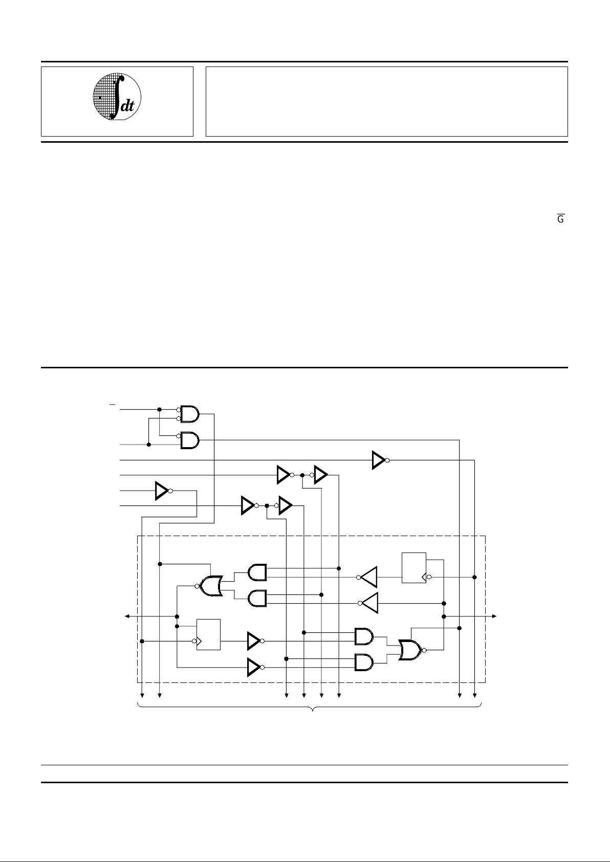
The IDT54/74FCT646/A/C consists of a bus transceiver
with 3-state D-type flip-flops and control circuitry arranged for
multiplexed transmission of data directly from the data bus or
from the internal storage registers.
The IDT54/74FCT646/A/C utilizes the enable control (G)
and direction (DIR) pins to control the transceiver functions.
SAB and SBA control pins are provided to select either real
time or stored data transfer. The circuitry used for select
control will eliminate the typical decoding glitch that occurs in
a multiplexer during the transition between stored and realtime data. A LOW input level selects real-time data and a
HIGH selects stored data.
Data on the A or B data bus or both can be stored in the
internal D flip flops by LOW-to-HIGH transitions at the
appropriate clock pins (CPAB or CPBA) regardless of the
select or enable control pins.
FAST CMOS OCTAL
TRANSCEIVER/REGISTER
FUNCTIONAL BLOCK DIAGRAM
2536 drw 01
1D
C1
A REG
A
1
1D
C1
B REG
B1
TO 7 OTHER CHANNELS
1 OF 8 CHANNELS
SAB
CPBA
CPAB
SBA
DIR
G
1
Page 2
7.18 2
IDT54/74FCT646/A/C
FAST CMOS OCTAL TRANSCEIVER/REGISTER MILITARY AND COMMERCIAL TEMPERATURE RANGES
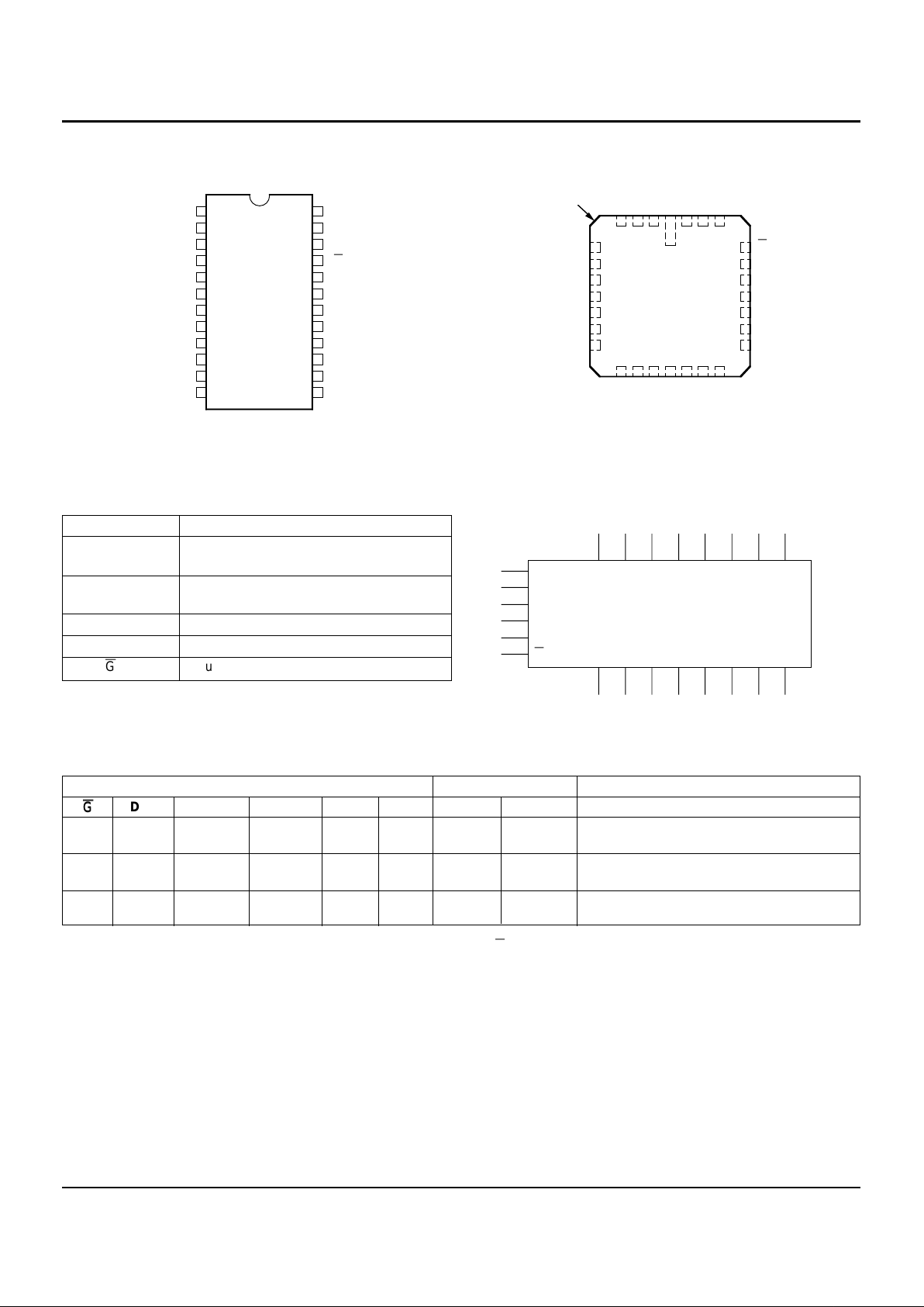
PIN CONFIGURATIONS
LCC
TOP VIEW
DIP/SOIC/CERPACK
TOP VIEW
FUNCTION TABLE
(2)
Inputs Data I/O
(1)
Operation or Function
G
G
DIR CPAB CPBA SAB SBA A
1–A8 B1–B8 IDT54/74FCT646
H X H or L H or L X X Input Input Isolation
HX ↑↑X X Store A and B Data
L L X X X L Output Input Real-Time B Data to A Bus
L L X H or L X H Stored B Data to A Bus
L H X X L X Input Output Real-Time A Data to B Bus
L H H or L X H X Stored A Data to B Bus
NOTES: 2536 tbl 02
1. The data output functions may be enabled or disabled by various signals at the G or DIR inputs. Data input functions are always enabled, i.e., data at
the bus pins will be stored on every LOW-to-HIGH transition on the clock inputs.
2. H = HIGH, L = LOW, X = Don’t Care, ↑ = LOW-to-HIGH Transition.
PIN DESCRIPTION
Pin Names Description
A
1–A8 Data Register A Inputs
Data Register B Outputs
B
1–B8 Data Register B Inputs
Data Register A Outputs
CPAB, CPBA Clock Pulse Inputs
SAB, SBA Output Data Source Select Inputs
DIR,
G
Output Enable Inputs
2536 tbl 01
LOGIC SYMBOL
5
6
7
8
9
10
11
12
GND
A
1
A
2
A
3
1
2
3
4
24
23
22
21
20
19
18
17
Vcc
16
15
14
13
CPAB
P24-1,
D24-1,
S024-2
&
E24-1
B
1
A
4
A
5
A
6
SAB
DIR
A
7
A
8
CPBA
SBA
G
B
2
B
3
B
4
B
5
B
6
B
7
B
8
2536 drw 06
CPAB
SAB
DIR
CPBA
SBA
G
A1B1A2B2A3B3A4B4A5B5A6B6A7B7A8
B8
5
6
7
8
9
10
11
L28-1
25
24
23
22
21
20
19
INDEX
2536 drw 02
B
1
G
B
2
B
3
B
4
B
5
NC
A
1
A
2
A
3
A
4
A
5
A
6
NC
Vcc
CPAB
SAB
DIR
CPBA
SBA
NC
GND
A
7A8
B8B7B
6
NC
12 13 14 15 16 17 18
432128 27 26
Page 3
IDT54/74FCT646/A/C
FAST CMOS OCTAL TRANSCEIVER/REGISTER MILITARY AND COMMERCIAL TEMPERATURE RANGES
7.18 3
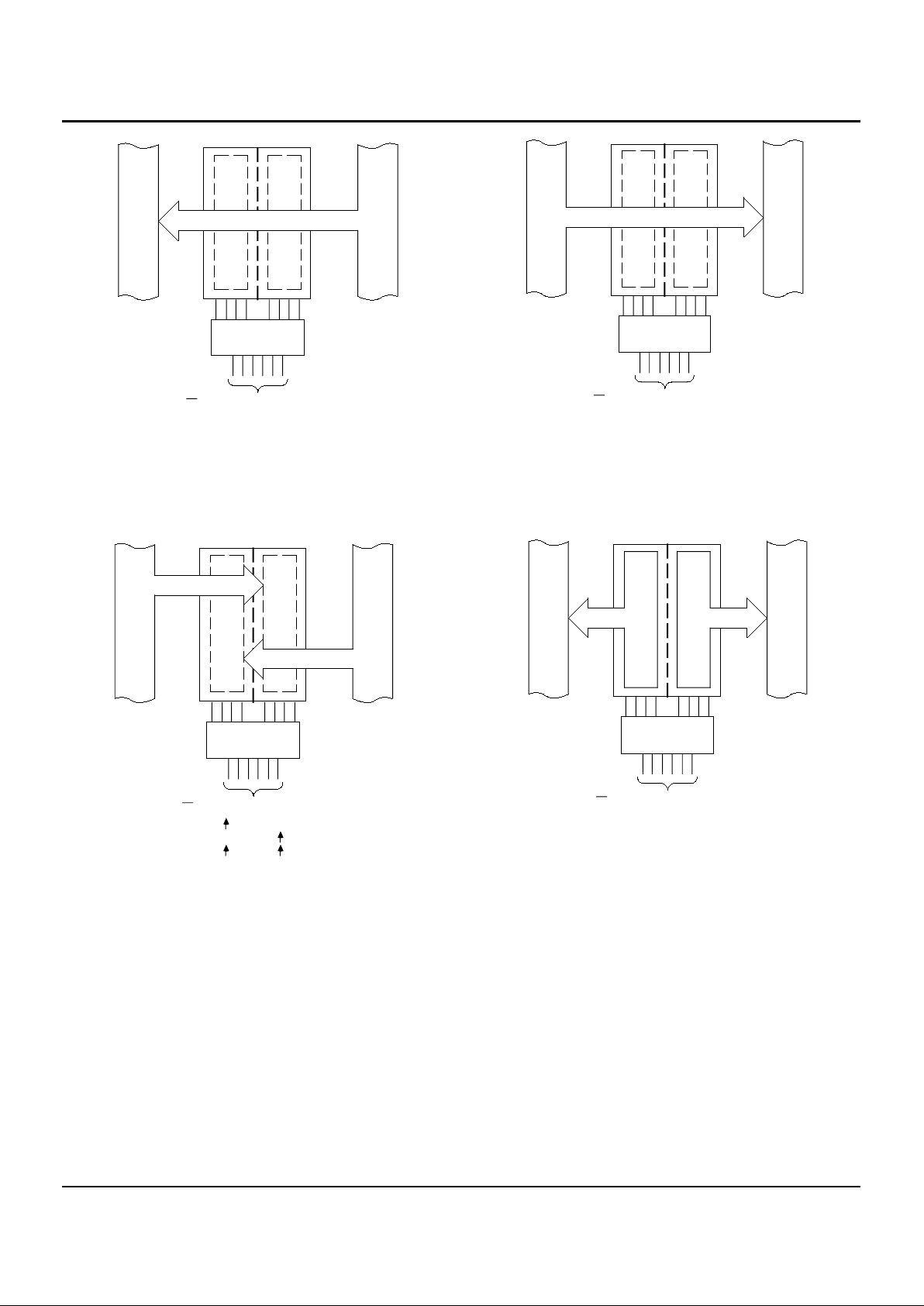
BUS
A
BUS
B
DIRLGLCPABXCPBAXSABXSBA
L
2536 drw 03
BUS
A
BUS
B
DIRHGLCPABXCPBAXSABLSBA
X
BUS
A
BUS
B
DIR
H
L
X
G
L
L
H
CPABXCPBAXSAB
X
X
X
SBA
X
X
X
2536 drw 04
BUS
A
BUS
B
DIR
L
H
G
L
L
CPAB
X
H or L
CPBA
H or L
X
SAB
X
H
SBA
H
X
(1)
STORAGE FROM
A AND/OR B
REAL–TIME TRANSFER
BUS B TO BUS A
REAL–TIME TRANSFER
BUS A TO BUS B
TRANSFER STORED
DATA TO A AND/OR B
NOTE:
1. Cannot transfer data to A bus and B bus simultaneously.
Page 4

7.18 4
IDT54/74FCT646/A/C
FAST CMOS OCTAL TRANSCEIVER/REGISTER MILITARY AND COMMERCIAL TEMPERATURE RANGES
ABSOLUTE MAXIMUM RATINGS
(1)
Symbol Rating Commercial Military Unit
V
TERM
(2)
Terminal Voltage –0.5 to +7.0 –0.5 to +7.0 V
with Respect
to GND
V
TERM
(3)
Terminal Voltage –0.5 to VCC –0.5 to VCC V
with Respect
to GND
T
A Operating 0 to +70 –55 to +125 °C
Temperature
T
BIAS Temperature –55 to +125 –65 to +135 °C
Under Bias
T
STG Storage –55 to +125 –65 to +150 °C
Temperature
P
T Power Dissipation 0.5 0.5 W
I
OUT DC Output Current 120 120 mA
NOTES: 2536 tbl 03
1. Stresses greater than those listed under ABSOLUTE MAXIMUM
RATINGS may cause permanent damage to the device. This is a stress
rating only and functional operation of the device at these or any other
conditions above those indicated in the operational sections of this
specification is not implied. Exposure to absolute maximum rating
conditions for extended periods may affect reliability. No terminal voltage
may exceed V
CC by +0.5V unless otherwise noted.
2. Inputs and V
CC terminals only.
3. Outputs and I/O terminals only.
CAPACITANCE (TA = +25°C, f = 1.0MHz)
Symbol Parameter
(1)
Conditions Typ. Max. Unit
C
IN Input Capacitance VIN = 0V 6 10 pF
C
I/O I/O Capacitance VOUT = 0V 8 12 pF
NOTE: 2536 tbl 04
1. This parameter is measured at characterization but not tested.
DC ELECTRICAL CHARACTERISTICS OVER OPERATING RANGE
Following Conditions Apply Unless Otherwise Specified: VLC = 0.2V; VHC = VCC – 0.2V
Commercial: TA = 0°C to +70°C, VCC = 5.0V ± 5%; Military: TA = –55°C to +125°C, VCC = 5.0V ± 10%
Symbol Parameter Test Conditions
(1)
Min. Typ.
(2)
Max. Unit
V
IH Input HIGH Level Guaranteed Logic HIGH Level 2.0 — — V
V
IL Input LOW Level Guaranteed Logic LOW Level — — 0.8 V
I
IH Input HIGH Current VCC = Max. VI = VCC ——5µA
(Except I/O pins) V
I = 2.7V — — 5
(4)
IIL Input LOW Current VI = 0.5V — — –5
(4)
(Except I/O pins) VI = GND — — –5
I
IH Input HIGH Current VCC = Max. VI = VCC ——15µA
(I/O pins only) V
I = 2.7V — — 15
(4)
IIL Input LOW Current VI = 0.5V — — –15
(4)
(I/O pins only) VI = GND — — –15
V
IK Clamp Diode Voltage VCC = Min., IN = –18mA — –0.7 –1.2 V
I
OS Short Circuit Current VCC = Max.
(3)
, VO = GND –60 –120 — mA
V
OH Output HIGH Voltage VCC = 3V, VIN = VLC or VHC, IOH = –32µAVHC VCC —V
V
CC = Min. IOH = –300µAVHC VCC —
V
IN = VIH or VIL IOH = –12mA MIL. 2.4 4.0 —
I
OH = –15mA COM’L. 2.4 4.0 —
V
OL Output LOW Voltage VCC = 3V, VIN = VLC or VHC, IOL = 300µA — GND VLC V
V
CC = Min. IOL = 300µA — GND VLC
(4)
VIN = VIH or VIL IOL = 48mA MIL. — 0.3 0.55
I
OL = 64mA COM’L. — 0.3 0.55
NOTES: 2536 tbl 05
1. For conditions shown as Max. or Min., use appropriate value specified under Electrical Characteristics for the applicable device type.
2. Typical values are at V
CC = 5.0V, +25°C ambient and maximum loading.
3. Not more than one output should be shorted at one time. Duration of the short circuit test should not exceed one second.
4. This parameter is guaranteed but not tested.
Page 5

IDT54/74FCT646/A/C
FAST CMOS OCTAL TRANSCEIVER/REGISTER MILITARY AND COMMERCIAL TEMPERATURE RANGES
7.18 5
POWER SUPPLY CHARACTERISTICS
VLC = 0.2V; VHC = VCC – 0.2V
Symbol Parameter Test Conditions
(1)
Min. Typ.
(2)
Max. Unit
I
CC Quiescent Power Supply Current VCC = Max. — 0.2 1.5 mA
V
IN ≥ VHC; VIN ≤ VLC
∆ICC Quiescent Power Supply Current VCC = Max. — 0.5 2.0 mA
TTL Inputs HIGH V
IN = 3.4V
(3)
ICCD Dynamic Power Supply Current
(4)
VCC = Max. VIN ≥ VHC — 0.15 0.25 mA/MHz
Outputs Open V
IN ≤ VLC
G
= DIR = GND
One Input Toggling
50% Duty Cycle
I
C Total Power Supply Current
(6)
VCC = Max. VIN ≥ VHC — 1.7 4.0 mA
Outputs Open V
IN ≤ VLC
fCP = 10MHz (FCT)
50% Duty Cycle
G
= DIR = GND V
IN = 3.4V — 2.2 6.0
One Bit Toggling V
IN = GND
at fi = 5MHz
50% Duty Cycle
V
CC = Max. VIN ≥ VHC — 7.0 12.8
(5)
Outputs Open VIN ≤ VLC
fCP = 10MHz (FCT)
50% Duty Cycle
G
= DIR = GND V
IN = 3.4V — 9.2 21.8
(5)
Eight Bits Toggling VIN = GND
at f
i = 5MHz
50% Duty Cycle
NOTES: 2536 tbl 06
1. For conditions shown as Max. or Min., use appropriate value specified under Electrical Characteristics for the applicable device type.
2. Typical values are at V
CC = 5.0V, +25°C ambient.
3. Per TTL driven input (V
IN = 3.4V); all other inputs at VCC or GND.
4. This parameter is not directly testable, but is derived for use in Total Power Supply calculations.
5. Values for these conditions are examples of the I
CC formula. These limits are guaranteed but not tested.
6. I
C = IQUIESCENT + IINPUTS + IDYNAMIC
IC = ICC + ∆ICC DHNT + ICCD (fCP/2 + fiNi)
ICC = Quiescent Current
∆I
CC = Power Supply Current for a TTL High Input (VIN = 3.4V)
D
H = Duty Cycle for TTL Inputs High
N
T = Number of TTL Inputs at DH
ICCD = Dynamic Current Caused by an Output Transition Pair (HLH or LHL)
f
CP = Clock Frequency for Register Devices (Zero for Non-Register Devices)
f
i = Input Frequency
N
i = Number of Inputs at fi
All currents are in milliamps and all frequencies are in megahertz.
Page 6

7.18 6
IDT54/74FCT646/A/C
FAST CMOS OCTAL TRANSCEIVER/REGISTER MILITARY AND COMMERCIAL TEMPERATURE RANGES
SWITCHING CHARACTERISTICS OVER OPERATING RANGE
54/74FCT646 54/74FCT646A 54/74FCT646C
Com’l. Mil. Com’l. Mil. Com’l. Mil.
Symbol Parameter Condition
(1)
Min.
(2)
Max. Min.
(2)
Max. Min.
(2)
Max. Min.
(2)
Max. Min.
(2)
Max. Min.
(2)
Max. Unit
tPLH Propagation CL = 50 pF 2.0 9.0 2.0 11.0 2.0 6.3 2.0 7.7 1.5 5.4 1.5 6.0 ns
t
PHL Delay RL = 500Ω
Bus to Bus
t
PZH Output Enable 2.0 14.0 2.0 15.0 2.0 9.8 2.0 10.5 1.5 7.8 1.5 8.9 ns
t
PZL Time
G
, DIR to
Bus
t
PHZ Output Disable 2.0 9.0 2.0 11.0 2.0 6.3 2.0 7.7 1.5 6.3 1.5 7.7 ns
t
PLZ Time
G
, DIR to
Bus
t
PLH Propagation 2.0 9.0 2.0 10.0 2.0 6.3 2.0 7.0 1.5 5.7 1.5 6.3 ns
t
PHL Delay Clock
to Bus
t
PLH Propagation 2.0 11.0 2.0 12.0 2.0 7.7 2.0 8.4 1.5 6.2 1.5 7.0 ns
t
PHL Delay SBA or
SAB to Bus
t
SU Set-up Time 4.0 — 4.5 — 2.0 — 2.0 — 2.0 — 2.0 — ns
HIGH or LOW
Bus to Clock
t
H Hold Time 2.0 — 2.0 — 1.5 — 1.5 — 1.5 — 1.5 — ns
HIGH or LOW
Bus to Clock
t
W Clock Pulse 6.0 — 6.0 — 5.0 — 5.0 — 5.0 — 5.0 — ns
Width HIGH or
LOW
NOTES: 2536 tbl 07
1. See test circuit and waveforms.
2. Minimum limits are guaranteed but not tested on Propagation Delays.
Page 7

IDT54/74FCT646/A/C
FAST CMOS OCTAL TRANSCEIVER/REGISTER MILITARY AND COMMERCIAL TEMPERATURE RANGES
7.18 7
TEST CIRCUITS AND WAVEFORMS
TEST CIRCUITS FOR ALL OUTPUTS
ENABLE AND DISABLE TIMESPROPAGATION DELAY
SET-UP, HOLD AND RELEASE TIMES PULSE WIDTH
Pulse
Generator
DATA
INPUT
TIMING
INPUT
ASYNCHRONOUS CONTROL
PRESET
CLEAR
ETC.
SYNCHRONOUS CONTROL
PRESET
CLEAR
CLOCK ENABLE
ETC.
3V
1.5V
0V
3V
1.5V
0V
3V
1.5V
0V
3V
1.5V
0V
t
SU
t
H
t
REM
H
tSU
RT
D.U.T.
VCC
VIN
CL
VOUT
50pF
500Ω
500Ω
7.0V
SAME PHASE
INPUT TRANSITION
3V
1.5V
0V
1.5V
V
OH
V
OL
t
PLH
t
PHL
OUTPUT
OPPOSITE PHASE
INPUT TRANSITION
CONTROL
INPUT
3V
1.5V
0V
3.5V
0V
OUTPUT
NORMALLY
LOW
OUTPUT
NORMALLY
HIGH
SWITCH
CLOSED
SWITCH
OPEN
V
OL
V
OH
3V
1.5V
0V
t
PLH
t
PHL
0.3V
0.3V
t
PLZ
t
PZL
t
PZH
t
PHZ
3.5V
0V
1.5V
1.5V
ENABLE DISABLE
HIGH-LOW-HIGH
PULSE
LOW-HIGH-LOW
PULSE
t
W
1.5V
1.5V
t
NOTES 2536 drw 07
1. Diagram shown for input Control Enable-LOW and input Control
Disable-HIGH.
2. Pulse Generator for All Pulses: Rate ≤ 1.0 MHz; Z
O ≤ 50Ω; tF ≤ 2.5ns;
t
R ≤ 2.5ns.
SWITCH POSITION
Test Switch
Open Drain
Disable Low Closed
Enable Low
All Other Tests Open
DEFINITIONS: 2536 tbl 08
CL = Load capacitance: includes jig and probe capacitance.
R
T = Termination resistance: should be equal to ZOUT of the Pulse
Generator.
Page 8

7.18 8
IDT54/74FCT646/A/C
FAST CMOS OCTAL TRANSCEIVER/REGISTER MILITARY AND COMMERCIAL TEMPERATURE RANGES
ORDERING INFORMATION
XX
PackageXProcess/
Temperature
Range
Blank
B
Commercial
MIL-STD-883, Class B
P
D
SO
L
E
Plastic DIP
CERDIP
Small Outline IC
Leadless Chip Carrier
CERPACK
646
646A
646C
Non-inverting Octal Transceiver/Register
Fast Non-inverting Octal Transceiver/Register
Super Fast Non-inverting Octal Transceiver/Register
XXXX
Device
Type
2536 drw 05
54
75
–55°C to +125°C
0°C to +70°C
FCT
Temperature
Range
XXIDT
 Loading...