

Datasheet IDT74LVCH16245APV, IDT74LVCH16245APF, IDT74LVCH16245APA Datasheet (Integrated Device Technology)
Page 1
IDT74LVCH16245A
3.3V CMOS 16-BIT BUS TRANSCEIVER WITH 3-STATE OUTPUTS
INDUSTRIAL TEMPERATURE RANGE
3.3V CMOS 16-BIT
BUS TRANSCEIVER
WITH 3-STATE OUTPUTS,
5 VOLT TOLERANT I/O AND BUS-HOLD
FEA TURES:
• Typical tSK(o) (Output Skew) < 250ps
• ESD > 2000V per MIL-STD-883, Method 3015; > 200V using
machine model (C = 200pF, R = 0)
•VCC = 3.3V ± 0.3V, Normal Range
•VCC = 2.7V to 3.6V, Extended Range
• CMOS power levels (0.4
• All inputs, outputs, and I/O are 5V tolerant
• Available in SSOP, TSSOP, and TVSOP packages
DRIVE FEA TURES:
• High Output Drivers: ±24mA
• Reduced system switching noise
APPLICA TIONS:
• 5V and 3.3V mixed voltage systems
• Data communication and telecommunication systems
µµ
µ W typ. static)
µµ
IDT74LVCH16245A
DESCRIPTION:
This 16-bit bus transceiver is built using advanced dual metal CMOS
technology. This high-speed, low power transceiver is ideal for asynchronous communication between two busses (A and B). The Direction and
Output Enable controls are designed to operate this device as either two
independent 8-bit transceivers or one 16-bit transceiver. The direction
control pin (DIR) controls the direction of data flow. The output enable pin
(OE) overrides the direction control and disables both ports. All inputs are
designed with hysteresis for improved noise margin.
All pins can be driven from either 3.3V or 5V devices. This feature allows
the use of this device as a translator in a mixed 3.3V/5V supply system.
The LVCH16245A has been designed with a ±24mA output driver. This
driver is capable of driving a moderate to heavy load while maintaining
speed performance.
The LVCH16245A has “bus-hold” which retains the inputs' last state
whenever the input goes to a high impedance. This prevents floating inputs
and eliminates the need for pull-up/down resistors.
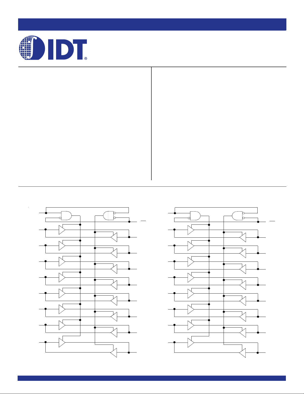
FUNCTIONAL BLOCK DIAGRAM
1
1DIR
47
1A1
46
1
A2
44
A3
1
43
A4
1
41
A5
1
40
A6
1
38
A7
1
37
A8
1
24
2DIR
48
1
OE
2
B1
1
3
1
B2
5
1
B3
6
1
B4
8
1
B5
9
1
B6
11
1
B7
12
B8
1
2A1
2
2
2
2
A6
2
2
A7
2
A2
A3
A4
A5
A8
36
35
33
32
30
29
27
26
25
2
OE
13
B1
2
14
2
B2
16
2
B3
17
2
B4
19
2
B5
20
2
B6
22
2
B7
23
B8
2
The IDT logo is a registered trademark of Integrated Device Technology, Inc.
MARCH 1999INDUSTRIAL TEMPERATURE RANGE
© 1999 Integrated Device Technology, Inc. DSC-4596/1
1
Page 2
IDT74LVCH16245A
3.3V CMOS 16-BIT BUS TRANSCEIVER WITH 3-STATE OUTPUTS
INDUSTRIAL TEMPERATURE RANGE
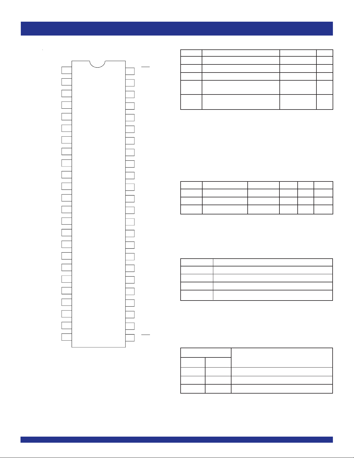
PIN CONFIGURATION
1DIR
1B1
1B2
GND
B3
1
1
B4
CC
V
1
B5
B6
1
GND
1
B7
1
B8
B1
2
2
B2
GND
2
3
4
5
6
7
8
9
10
11
12
13
14
15
481
47
46
45
44
43
42
41
40
39
38
37
36
35
34
1OE
1A1
1A2
GND
A3
1
1
A4
CC
V
1
A5
1
A6
GND
1
A7
A8
1
2
A1
2
A2
GND
ABSOLUTE MAXIMUM RATINGS
Symbol Description Max Unit
VTERM Terminal Voltage with Respect to GND –0.5 to +6.5 V
TSTG Storage Temperature –65 to +150 °C
IOUT DC Output Current –50 to +50 mA
I
IK Continuous Clamp Current, –50 mA
IOK VI < 0 or VO < 0
I
CC Continuous Current through each ±100 mA
ISS VCC or GND
NOTE:
1. Stresses greater than those listed under ABSOLUTE MAXIMUM RATINGS may cause
permanent damage to the device. This is a stress rating only and functional operation
of the device at these or any other conditions above those indicated in the operational
sections of this specification is not implied. Exposure to absolute maximum rating
conditions for extended periods may affect reliability.
(1)
CAPACITANCE (TA = +25°C, F = 1.0MHz)
Symbol Parameter
CIN Input Capacitance VIN = 0V 4.5 6 pF
COUT Output Capacitance VOUT = 0V 6.5 8 pF
C
I/O I/O Port Capacitance VIN = 0V 6.5 8 pF
NOTE:
1. As applicable to the device type.
(1)
Conditions Typ. Max. Unit
2B3
B4
2
VCC
B5
2
2
B6
GND
B7
2
2B8
DIR
2
16
17
18
19
20
21
22
23
24
SSOP/ TSSOP/ TVSOP
TOP VIEW
33
32
31
30
29
28
27
26
25
2A3
2
A4
VCC
A5
2
2
A6
GND
2
A7
2A8
OE
2
PIN DESCRIPTION
Pin Names Description
xOE Output Enable Inputs (Active LOW)
xDIR Direction Control Input
xAx Side A Inputs or 3-State Outputs
xBx Side B Inputs or 3-State Outputs
NOTE:
1. These pins have "Bus-Hold". All other pins are standard inputs, outputs, or I/Os.
FUNCTION T ABLE (EACH 8-BIT SECTION)
Inputs
xOE xDIR Outputs
L L Bus B Data to Bus A
L H Bus A Data to Bus B
H X Isolation
NOTES:
1. H = HIGH Voltage Level
X = Don’t Care
L = LOW Voltage Level
(1)
(1)
(1)
2
Page 3

IDT74LVCH16245A
3.3V CMOS 16-BIT BUS TRANSCEIVER WITH 3-STATE OUTPUTS
INDUSTRIAL TEMPERATURE RANGE
DC ELECTRICAL CHARACTERISTICS OVER OPERATING RANGE
Following Conditions Apply Unless Otherwise Specified:
Operating Condition: TA = –40°C to +85°C
Symbol Parameter Test Conditions Min. Typ.
VIH Input HIGH Voltage Level VCC = 2.3V to 2.7V 1.7 — — V
VCC = 2.7V to 3.6V 2 — —
IL Input LOW Voltage Level VCC = 2.3V to 2.7V — — 0.7 V
V
VCC = 2.7V to 3.6V — — 0.8
IH Input Leakage Current VCC = 3.6V VI = 0 to 5.5V — — ±5µA
I
IIL
IOZH High Impedance Output Current VCC = 3.6V VO = 0 to 5.5V — — ±10 µA
IOZL (3-State Output pins)
IOFF Input/Output Power Off Leakage VCC = 0V, VIN or VO ≤ 5.5V — — ±50 µA
VIK Clamp Diode Voltage VCC = 2.3V, IIN = –18mA — –0.7 –1.2 V
VH Input Hysteresis VCC = 3.3V — 100 — mV
I
CCL Quiescent Power Supply Current VCC = 3.6V VIN = GND or VCC —— 10µA
ICCH
ICCZ 3.6 ≤ VIN ≤ 5.5V
(2)
—— 10
∆ICC Quiescent Power Supply Current One input at VCC - 0.6V, other inputs at VCC or GND — — 500 µA
Variation
(1)
Max. Unit
NOTES:
1. Typical values are at VCC = 3.3V, +25°C ambient.
2. This applies in the disabled state only.
BUS-HOLD CHARACTERISTICS
Symbol Parameter
(1)
Test Conditions Min. Typ.
IBHH Bus-Hold Input Sustain Current VCC = 3V VI = 2V – 75 — — µ A
IBHL VI = 0.8V 75 — —
IBHH Bus-Hold Input Sustain Current VCC = 2.3V VI = 1.7V — — — µ A
IBHL VI = 0.7V — — —
IBHHO Bus-Hold Input Overdrive Current VCC = 3.6V VI = 0 to 3.6V — — ±500 µA
IBHLO
NOTES:
1. Pins with Bus-Hold are identified in the pin description.
2. Typical values are at VCC = 3.3V, +25°C ambient.
(2)
Max. Unit
3
Page 4

IDT74LVCH16245A
3.3V CMOS 16-BIT BUS TRANSCEIVER WITH 3-STATE OUTPUTS
INDUSTRIAL TEMPERATURE RANGE
OUTPUT DRIVE CHARACTERISTICS
Symbol Parameter Test Conditions
VOH Output HIGH Voltage VCC = 2.3V to 3.6V IOH = – 0.1mA VCC – 0.2 — V
CC = 2.3V IOH = – 6mA 2 —
V
V
CC = 2.3V IOH = – 12mA 1.7 —
VCC = 2.7V 2.2 —
VCC = 3V 2.4 —
VCC = 3V IOH = – 24mA 2.2 —
OL Output LOW Voltage VCC = 2.3V to 3.6V IOL = 0.1mA — 0.2 V
V
V
CC = 2.3V IOL = 6mA — 0.4
VCC = 2.7V IOL = 12mA — 0.4
VCC = 3V IOL = 24mA — 0.55
NOTE:
1. VIH and VIL must be within the min. or max. range shown in the DC ELECTRICAL CHARACTERISTICS OVER OPERATING RANGE table for the appropriate VCC range.
TA = – 40°C to + 85°C.
(1)
Min. Max. Unit
IOL = 12mA — 0.7
OPERA TING CHARACTERISTICS, VCC = 3.3V ± 0.3V , TA = 25°C
Symbol Parameter Test Conditions Typical Unit
CPD Power Dissipation Capacitance per Transceiver Outputs enabled CL = 0pF, f = 10Mhz 40 pF
CPD Power Dissipation Capacitance per Transceiver Outputs disabled 4
SWITCHING CHARACTERISTICS
(1)
VCC = 2.7V VCC = 3.3V ± 0.3V
Symbol Parameter Min. Max. Min. Max. Unit
tPLH Propagation Delay — 4.7 1 4 ns
tPHL xAx to xBx, xBx to xAx
tPZH Output Enable Time — 6.7 1.5 5.5 ns
tPZL xOE to xAx or xBx
tPHZ Output Disable Time — 7.1 1.5 6.6 ns
tPLZ xOE to xAx or xBx
tSK( o) Output Skew
NOTES:
1. See TEST CIRCUITS AND WAVEFORMS. TA = – 40°C to + 85°C.
2. Skew between any two outputs of the same package and switching in the same direction.
(2)
——— 1ns
4
Page 5

IDT74LVCH16245A
3.3V CMOS 16-BIT BUS TRANSCEIVER WITH 3-STATE OUTPUTS
TEST CIRCUITS AND WAVEFORMS
INDUSTRIAL TEMPERATURE RANGE
TEST CONDITIONS
Symbol VCC
(1)
= 3.3V±0.3V VCC
VLOAD 6 6 2 x Vcc V
VIH 2.7 2.7 Vcc V
VT 1.5 1.5 Vcc / 2 V
VLZ 300 300 150 mV
VHZ 300 300 150 mV
L 50 50 30 pF
C
VIN
(1, 2)
Pulse
Generator
Test Circuit for All Outputs
DEFINITIONS:
CL = Load capacitance: includes jig and probe capacitance.
RT = Termination resistance: should be equal to ZOUT of the Pulse Generator.
NOTES:
1. Pulse Generator for All Pulses: Rate ≤ 10MHz; tF ≤ 2.5ns; tR ≤ 2.5ns.
2. Pulse Generator for All Pulses: Rate ≤ 10MHz; tF ≤ 2ns; tR ≤ 2ns.
RT
VCC
D.U.T.
(1)
= 2.7V VCC
VOUT
(2)
= 2.5V±0.2V Unit
500Ω
500Ω
CL
LVC Link
VLOAD
Open
GND
SAME PHASE
INPUT TRANSITION
OUTPUT
OPPOSITE PHASE
INPUT TRANSITION
tPLH
tPLH
tPHL
tPHL
VIH
VT
0V
V
VT
VOL
VIH
VT
0V
LVC Link
OH
Propagation Delay
DISABLE
tPLZ
tPHZ
VIH
VT
0V
VLOAD/2
V
VOL
VOH
VOH-VHZ
0V
LVC Link
OL+VLZ
CONTROL
INPUT
OUTPUT
NORMALLY
LOW
OUTPUT
NORMALLY
HIGH
ENABLE
tPZL
SWITCH
CLOSED
tPZH
SWITCH
OPEN
VLOAD/2
VT
VT
0V
Enable and Disable Times
NOTE:
1. Diagram shown for input Control Enable-LOW and input Control Disable-HIGH.
SWITCH POSITION
Test Switch
Open Drain
Disable Low V
Enable Low
Disable High GND
Enable High
All Other Tests Open
INPUT
OUTPUT 1
tPLH1
tSK (x)
OUTPUT 2
tPLH2
tSK(x) = tPLH2 - tPLH1 or tPHL2 - tPHL1
Output Skew - tSK(X)
NOTES:
1. For tSK(o) OUTPUT1 and OUTPUT2 are any two outputs.
2. For tSK(b) OUTPUT1 and OUTPUT2 are in the same bank.
t
PHL1
tSK (x)
tPHL2
LOAD
VIH
VT
0V
V
OH
VT
VOL
VOH
VT
VOL
LVC Link
TIMING
ASYNCHRONOUS
CONTROL
SYNCHRONOUS
CONTROL
LOW-HIGH-LOW
HIGH-LOW-HIGH
5
DATA
INPUT
t
SU
INPUT
tSU
Set-up, Hold, and Release Times
PULSE
tW
PULSE
Pulse Width
tREM
tH
VIH
VT
tH
0V
VIH
VT
0V
VIH
VT
0V
VIH
VT
0V
LVC Link
VT
VT
LVC Link
Page 6

IDT74LVCH16245A
3.3V CMOS 16-BIT BUS TRANSCEIVER WITH 3-STATE OUTPUTS
ORDERING INFORMATION
INDUSTRIAL TEMPERATURE RANGE
IDT
Temp. Range
XX
LVC
XXX
FamilyBus-Hold
XXXX
XX
PackageDevice Type
PV
PA
PF
245A
16
H
74
Shrink Small Outline Package
Thin Shrink Small Outline Package
Thin Very Small Outline Package
16-Bit Bus Transceiver with 3-State Outputs
Double-Density, ±24mA
Bus-hold
-40°C to +85°C
CORPORATE HEADQUARTERS for SALES: for Tech Support:
2975 Stender Way 800-345-7015 or 408-727-6116 logichelp@idt.com
Santa Clara, CA 95054 fax: 408-492-8674 (408) 654-6459
www.idt.com
6
 Loading...