

Datasheet IDT74FCT88915TT133PYB, IDT74FCT88915TT133LB, IDT74FCT88915TT133L, IDT74FCT88915TT133JB, IDT74FCT88915TT133J Datasheet (Integrated Device Technology)
...Page 1
IDT54/74FCT88915TT 55/70/100/133
LOW SKEW PLL-BASED CLOCK DRIVER MILITARY AND COMMERCIAL TEMPERATURE RANGES
LOW SKEW PLL-BASED
CMOS CLOCK DRIVER
Integrated Device Technology, Inc.
FEATURES:
• 0.5 MICRON CMOS Technology
• Input frequency range: 10MHz – f2Q Max. spec
(FREQ_SEL = HIGH)
• Max. output frequency: 133MHz
• Pin and function compatible with MC88915T
• 5 non-inverting outputs, one inverting output, one 2x
output, one ÷2 output; all outputs are TTL-compatible
• 3-State outputs
• Output skew < 500ps (max.)
• Duty cycle distortion < 500ps (max.)
• Part-to-part skew: 1ns (from t
PD max. spec)
• TTL level output voltage swing
• 64/–15mA drive at TTL output voltage levels
• Available in 28 pin PLCC, LCC and SSOP packages
DESCRIPTION:
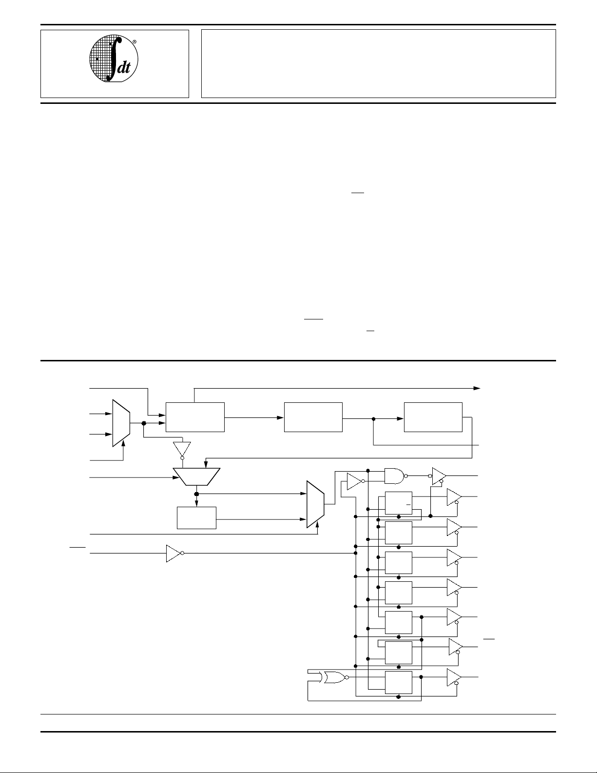
The IDT54/74FCT88915TT uses phase-lock loop technology to lock the frequency and phase of outputs to the input
reference clock. It provides low skew clock distribution for
high performance PCs and workstations. One of the outputs
(WITH 3-STATE)
IDT54/74FCT88915TT
55/70/100/133
PRELIMINARY
is fed back to the PLL at the FEEDBACK input resulting in
essentially delay across the device. The PLL consists of the
phase/frequency detector, charge pump, loop filter and VCO.
The VCO is designed for a 2Q operating frequency range of
40MHz to f2Q Max.
The IDT54/74FCT88915TT provides 8 outputs with 500ps
skew. The
runs at twice the Q frequency and Q/2 runs at half the Q
frequency.
The FREQ_SEL control provides an additional ÷ 2 option in
the output path. PLL _EN allows bypassing of the PLL, which
is useful in static test modes. When PLL_EN is low, SYNC
input may be used as a test clock. In this test mode, the input
frequency is not limited to the specified range and the polarity
of outputs is complementary to that in normal operation
(PLL_EN = 1). The LOCK output attains logic HIGH when the
PLL is in steady-state phase and frequency lock. When OE/
RST is low, all the outputs are put in high impedance state and
registers at Q, Q and Q/2 outputs are reset.
The IDT54/74FCT88915TT requires one external loop
filter component as recommended in Figure 1.
Q5 output is inverted from the Q outputs. The 2Q
FUNCTIONAL BLOCK DIAGRAM
FEEDBACK
SYNC (0)
SYNC (1)
0
M
u
x
1
Phase/Freq.
Detector
Charge Pump
Voltage
Controlled
Oscilator
REF_SEL
PLL_EN
FREQ_SEL
OE/RST
The IDT logo is a registered trademark of Integrated Device Technology, Inc.
01
Mux
Divide
-By-2
(
(
÷1)
÷2)
1
M
u
x
0
D
D
CP
CP
D
CP
D
CP
D
CP
D
CP
D
CP
D
CP
Q
Q
Q
Q
R
Q
R
Q
R
Q
R
Q
R
Q
R
Q
R
MILITARY AND COMMERCIAL TEMPERATURE RANGES AUGUST 1995
1995 Integrated Device Technology, Inc. 9.7 DSC-4247/1
9.7 1
LOCK
LF
2Q
Q0
Q1
Q2
Q3
Q4
Q5
Q/2
3072 drw 01
1
Page 2
IDT54/74FCT88915TT 55/70/100/133
LOW SKEW PLL-BASED CMOS CLOCK DRIVER MILITARY AND COMMERCIAL TEMPERATURE RANGES
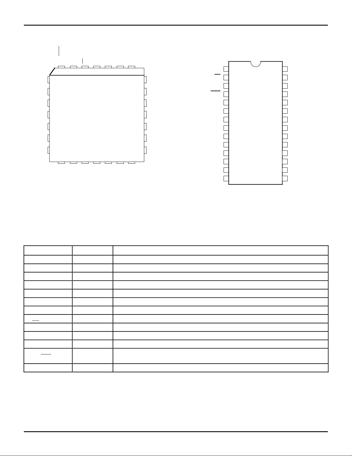
PIN CONFIGURATIONS
FEEDBK
REF_SEL
SYNC(0)
V
CC
(AN)
LF
GND(AN)
SYNC(1)
CC
OE/RST
Q5
V
GND
Q4
284 3 2 1 27 26
5
6
7
8
J28-1,
L28-1
9
10
11
12 13 14 15 16 17 18
CC
GND
Q0
Q1
V
FREQ_SEL
PLCC/LCC
TOP VIEW
CC
V
GND
2Q
25
24
23
22
21
20
19
PLL_EN
3072 drw 02
Q/2
GND
Q3
V
CC
Q2
GND
LOCK
GND
Q5
V
CC
OE/RST
FEEDBACK
REF_SEL
SYNC(0)
V
CC
(AN)
LF
GND(AN)
SYNC(1)
FREQ_SEL
GND
Q0
1
2
3
4
5
6
7
8
9
10
11
12
13
SO28-7
SSOP
TOP VIEW
28
27
26
25
24
23
22
21
20
19
18
17
16
1514
Q4
CC
V
2Q
Q/2
GND
Q3
V
CC
Q2
GND
LOCK
PLL_EN
GND
Q1
CC
V
3072 drw 03
PIN DESCRIPTION
Pin Name I/O Description
SYNC(0) I Reference clock input.
SYNC(1) I Reference clock input.
REF_SEL I Chooses reference between SYNC (0) & SYNC (1). (Refer to functional block diagram).
FREQ_SEL I Selects between ÷1 and ÷2 frequency options. (Refer to functional block diagram).
FEEDBACK I Feedback input to phase detector.
LF I Input for external loop filter connection.
Q0-Q4 O Clock output.
Q5
2Q O Clock output (2 x Q frequency).
Q/2 O Clock output (Q frequency ÷ 2).
LOCK O Indicates phase lock has been achieved (HIGH when locked).
OE/RST
PLL_EN I Disables phase-lock for low frequency testing. (Refer to functional block diagram).
O Inverted clock output.
I Asynchronous reset (active LOW) and output enable (active HIGH). When HIGH, outputs are
enabled. When LOW, outputs are in HIGH impedance.
3072 tbl 01
9.7 2
Page 3
IDT54/74FCT88915TT 55/70/100/133
LOW SKEW PLL-BASED CLOCK DRIVER MILITARY AND COMMERCIAL TEMPERATURE RANGES
ABSOLUTE MAXIMUM RATINGS
(1)
Symbol Rating Commercial Military Unit
(2)
VTERM
Terminal Voltage
–0.5 to +7.0 –0.5 to +7.0 V
with Respect to
GND
(3)
VTERM
TA Operating
Terminal Voltage
with Respect to
GND
–0.5 to V
+0.5
CC
–0.5 to V
CC
+0.5
0 to +70 –55 to +125 °C
V
Temperature
TBIAS Temperature
–55 to +125 –65 to +135 °C
Under Bias
TSTG Storage
–55 to +125 –65 to +150 °C
Temperature
IOUT DC Output
–60 to +120 –60 to +120 mA
Current
NOTES:
1. Stresses greater than those listed under ABSOLUTE MAXIMUM RATINGS may cause permanent damage to the device. This is a stress rating
only and functional operation of the device at these or any other conditions
above those indicated in the operational sections of this specification is
not implied. Exposure to absolute maximum rating conditions for
extended periods may affect reliability. No terminal voltage may exceed
CC by +0.5V unless otherwise noted.
V
2. Input and V
3. Output and I/O terminals.
CC terminals.
3072 tbl 02
CAPACITANCE (TA = +25°C, f = 1.0MHz)
Symbol Parameter
C
IN
Input
Capacitance
C
OUT
Output
Capacitance
NOTE:
1. This parameter is measured at characterization but not tested.
(1)
Conditions Typ. Max. Unit
VIN = 0V 4.5 6.0
V
OUT
= 0V 5.5 8.0
pF
pF
3072 lnk 03
DC ELECTRICAL CHARACTERISTICS OVER OPERATING RANGE
Following Conditions Apply Unless Otherwise Specified:
Commercial: T
Symbol Parameter Test Conditions
VIH Input HIGH Level Guaranteed Logic HIGH Level 2.0 — — V
VIL Input LOW Level Guaranteed Logic LOW Level — — 0.8 V
II H Input HIGH Current VCC = Max. VI = VCC ——±1µA
II L Input LOW Current VI = GND — — ±1 µA
IOZH High Impedance Output Current VCC = Max. VO = 2.7V — — ±1 µA
IOZL VO = 0.5V — — ±1 µA
VIK Clamp Diode Voltage VCC = Min., IIN = –18mA — –0.7 –1.2 V
VH Input Hysteresis — — 100 — mV
VOH Output HIGH Voltage VCC = Min. IOH = –3mA 2.5 3.5 — V
VOL Output LOW Voltage VCC = Min.
ICCL
ICCH
ICCZ
NOTES:
1. For conditions shown as Max. or Min., use appropriate value specified under Electrical Characteristics for the applicable device type.
2. Typical values are at Vcc = 5.0V, +25°C ambient.
3. Duration of the condition can not exceed one second.
A = 0°C to 70°C, VCC = 5.0V ± 5%
(1)
VIN = VIH or VIL IOH = –12mA MIL.
OH = –15mA COM'L.
I
IOH = –24mA MIL.
OH = –32mA COM'L.
I
IOL = 48mA MIL.
IN = VIH or VIL
V
OL = 64mA COM'L.
I
Quiescent Power Supply Current VCC = Max., VIN = GND or VCC
(Test mode)
(3)
Min. Typ.
(2)
Max. Unit
2.4 3.5 — V
2.0 3.0 — V
— 0.2 0.55 V
— 2.0 4.0 mA
3072 tbl 04
9.7 3
Page 4

IDT54/74FCT88915TT 55/70/100/133
LOW SKEW PLL-BASED CMOS CLOCK DRIVER MILITARY AND COMMERCIAL TEMPERATURE RANGES
POWER SUPPLY CHARACTERISTICS
Symbol Parameter Test Conditions
∆ICC Quiescent Power Supply Current
TTL Inputs HIGH
ICCD Dynamic Power Supply
(4)
Current
VCC = Max.
V
IN = VCC –2.1V
VCC = Max.
All Outputs Open
(3)
(1)
VIN = VCC
V
IN = GND
Min. Typ.
— 0.5 1.5 mA
— 0.25 0.4 mA/
CPD Power Dissipation Capacitance 50% Duty Cycle — 15 40 pF
IC Total Power Supply Current
(5,6)
VCC = Max.
—2540mA
PLL_EN = 1, LOCK = 1, FEEDBACK = Q/2
SYNC frequency = 20MHz. Q/2 loaded with 50pF
All other outputs open
VCC = Max.
—4260mA
PLL_EN = 1, LOCK = 1, FEEDBACK = Q/2
SYNC frequency = 20MHz. Q/2 loaded with 50Ω
Thevenin termination. All other outputs open
NOTES:
1. For conditions shown as Max. or Min., use appropriate value specified under Electrical Characteristics.
2. Typical values are at V
3. Per TTL driven input; all other inputs at V
4. This parameter is not directly testable, but is derived for use in Total Power Supply Calculations. It is derived with Q frequency as the reference.
5. Values for these conditions are examples of the I
6. I
C = IQUIESCENT + IINPUTS + IDYNAMIC
IC = ICC + ∆ICC DHNT + ICCD (f) + ILOAD
ICC = Quiescent Current (ICCL, ICCH and ICCZ)
CC = Power Supply Current for a TTL High Input
∆I
H = Duty Cycle for TTL Inputs High
D
N
T = Number of TTL Inputs at DH
ICCD = Dynamic Current Caused by an Input Transition Pair (HLH or LHL)
f = 2Q frequency
LOAD = Dynamic Current due to load.
I
CC = 5.0V, +25°C ambient.
CC or GND.
CC formula. These limits are guaranteed but not tested.
(2)
Max. Unit
MHz
3072 tbl 05
SYNC INPUT TIMING REQUIREMENTS
Symbol Parameter Min. Max. Unit
TRISE/FALL Rise/Fall Times,
— 3.0 ns
SYNC inputs
(0.8V to 2.0V)
Frequency Input Frequency,
10
(1)
2Q fmax MHz
SYNC Inputs
Duty Cycle Input Duty Cycle,
25% 75% —
SYNC Inputs
3053 tbl 06
OUTPUT FREQUENCY SPECIFICATIONS
Max.
Symbol Parameter Min. 55 70 100 133 Unit
f2Q Operating frequency 2Q Output 40 55 70 100 133 MHz
fQ
Operating frequency Q0-Q4,
Q5 Outputs
20 27.5 35 50 66.7 MHz
fQ/2 Operating frequency Q/2 Output 10 13.75 17.5 25 33.3 MHz
NOTES:
1. Note 8 in "General AC Specification Notes" and Figure 2 describes this specification and its actual limits depending on the feedback connection.
2. Maximum operating frequency is guaranteed with the part in a phase locked condition and all outputs loaded.
(2)
3072 tbl 07
9.7 4
Page 5

IDT54/74FCT88915TT 55/70/100/133
LOW SKEW PLL-BASED CLOCK DRIVER MILITARY AND COMMERCIAL TEMPERATURE RANGES
SWITCHING CHARACTERISTICS OVER OPERATING RANGE
Symbol Parameter Condition
tRISE/FALL
All outputs
tPULSE WIDTH
All outputs
(3)
(3)
tPD
SYNC-FEEDBACK
Rise/Fall Time
(between 0.8V and 2.0V)
Output Pulse Width
Q0-Q4,
Q5, Q/2, 2Q @ 1.5V
SYNC input to FEEDBACK delay
(3)
(measured at SYNC0 or 1 and FEEDBACK
input pins)
Load = 50Ω to
VCC/2, CL = 20pF
Load = 50Ω to
V
CC/2, CL = 20pF
0.1µF from LF to
Analog GND
tSKEWr
(rising)
(3,4)
Output to Output Skew
between outputs 2Q, Q0-Q4,
Load = 50Ω to
V
CC/2, CL = 20pF
Q/2 (rising edges only)
tSKEWf
(falling)
tSKEWall
(6)
tLOCK
(3,4)
(3,4)
Output to Output Skew
Time required to acquire
Output to Output Skew
between outputs Q0-Q4 (falling edges only)
2Q, Q/2, Q0-Q4 rising,
Q5 falling
Phase-Lock from time
SYNC input signal is received
tPZH
tPZL
tPHZ
tPLZ
GENERAL AC SPECIFICATION NOTES:
1. See test circuit and waveforms.
2. Minimum limits are guaranteed but not tested.
3. These specifications are guaranteed but not production tested.
4. Under equally loaded conditions, as specified under test conditions, and at a fixed temperature and voltage.
5. t
CYCLE = 1/frequency at which each output (Q, Q, Q/2 or 2Q) is expected to run.
6. With V
CC fully powered-on and an output properly connected to the FEEDBACK pin. tLOCK Max. is with C1 = 0.1µF, tLOCK Min. is with C1 = 0.01µF.
(Where C1 is loop filter capacitor shown in Figure 1).
Output Enable Time
RST (LOW-to-HIGH) to Q, 2Q, Q/2, Q
OE/
Output Disable Time
RST (HIGH-to-LOW) to Q, 2Q, Q/2, Q
OE/
(1)
(9)
Min. Max. Unit
(2)
0.2
1.2 ns
0.5t
CYCLE – 0.5
(5)
0.5tCYCLE + 0.5
–0.5 +0.5 ns
— 350 ps
— 350 ps
— 500 ps
(2)
1
10 ms
(2)
3
14 ns
(2)
3
14 ns
(5)
3072 tbl 08
ns
9.7 5
Page 6

IDT54/74FCT88915TT 55/70/100/133
LOW SKEW PLL-BASED CMOS CLOCK DRIVER MILITARY AND COMMERCIAL TEMPERATURE RANGES
NOTES:
7. These two specs ( t
RISE/FALL and tPULSE WIDTH 2Q output) guarantee that the FCT88915TT meets 68040 P-Clock input specification.
88915TT
2Q
Output
Zo (clock trace)
Rp
68040
P-Clock
Input
Rp = 1.5 Zo
3072 drw 04
8. The wiring diagrams and written explanations of Figure 4 demonstrate the input and output frequency relationships for various possible feedback
configurations. The allowable SYNC input range to stay in the phase-locked condition is also indicated. There are two allowable SYNC frequency ranges,
depending on whether FREQ_SEL is HIGH or LOW. Also it is possible to feed back the
input and the Q outputs. The table below summarizes the allowable SYNC frequency range for each possible configuration.
FREQ_SEL
Level
HIGH Q/2 10 to (2Q fMAX Spec)/4 40 to (2Q fMAX Spec) 0°
HIGH Any Q (Q0-Q4) 20 to (2Q fMAX Spec)/2 40 to (2Q fMAX Spec) 0°
HIGH
HIGH 2Q 40 to (2Q fMAX Spec) 40 to (2Q fMAX Spec) 0°
LOW Q/2 5 to (2Q fMAX Spec)/8 20 to (2Q fMAX Spec)/2 0°
LOW Any Q (Q0-Q4) 10 to (2Q fMAX Spec)/4 20 to (2Q fMAX Spec)/2 0°
LOW
LOW 2Q 20 to (2Q fMAX Spec)/2 20 to (2Q fMAX Spec)/2 0°
9. The tPD spec describes how the phase offset between the SYNC input and the output connected to the FEEDBACK input, varies with process, temperature
and voltage. Measurements were made with a 10MHz SYNC input and Q/2 output as feedback. The phase measurements were made at 1.5V.
The Q/2 output was terminated at the FEEDBACK input with 100Ω to V
tPD measurements were made with the loop filter connection shown below:
Feedback
Output
Q5
Q5
Allowable SYNC Input
Frequency Range (MH
20 to (2Q f
10 to (2Q f
MAX Spec)/2 40 to (2Q fMAX Spec) 180°
MAX Spec)/4 20 to (2Q fMAX Spec)/2 180°
CC and 100Ω to ground.
Z)
Q5 output, thus creating a 180° phase shift between the SYNC
Phase Relationship
Corresponding 2Q output
Frequency Range
of the Q Outputs
to Rising SYNC Edge
3072 tbl 09
External Loop
Filter
LF
0.1µFC1
Analog GND
3072 drw 05
9.7 6
Page 7

IDT54/74FCT88915TT 55/70/100/133
LOW SKEW PLL-BASED CLOCK DRIVER MILITARY AND COMMERCIAL TEMPERATURE RANGES
BOARD VCC
10µF
Low
Freq.
Bypass
0.1µF
High
Freq.
Bypass
0.1µF (Loop
ANALOG V
Analog loop filter
LF
section of the
FCT88915TT
CC
Filter Cap)
ANALOG GND
BOARD GND
A separate Analog power supply is not necessary
and should not be used. Following these prescribed
guidelines is all that is necessary to use the
FCT88915TT in a normal digital environment.
3072 drw 06
Figure 1. Recommended Loop Filter and Analog Isolation Scheme for the FCT88915TT
NOTES:
1. Figure 1 shows a loop filter and analog isolation scheme which will be effective in most applications. The following guidelines should be followed to ensure
stable and jitter-free operation:
a. All loop filter and analog isolation components should be tied as close to the package as possible. Stray current passing through the parasitics of
long traces can cause undesirable voltage transients at the LF pin.
b. The 10µF low frequency bypass capacitor and the 0.1µF high frequency bypass capacitor form a wide bandwidth filter that will minimize the
88915TT's sensitivity to voltage transients from the system digital V
If good bypass techniques are used on a board design near components which may cause digital V
not occur at the 88915TT's digital V
protection from the power supply and ground plane transients that can occur in a high frequency, high speed digital system.
c. The loop filter capacitor (0.1µF) can be a ceramic chip capacitor, the same as a standard bypass capacitor.
2. In addition to the bypass capacitors used in the analog filter of figure 1 there should be a 0.1µF bypass capacitor between each of the other (digital) four
V
CC pins and the board ground plane. This will reduce output switching noise caused by the 88915TT outputs, in addition to reducing potential for noise
in the "analog" section of the chip. These bypass capacitors should also be tied as close to the 88915TT package as possible.
CC supply. The purpose of the bypass filtering scheme shown in figure 1 is to give the 88915TT additional
CC supply and ground planes.
CC and ground noise, VCC step deviations should
9.7 7
Page 8

IDT54/74FCT88915TT 55/70/100/133
LOW SKEW PLL-BASED CMOS CLOCK DRIVER MILITARY AND COMMERCIAL TEMPERATURE RANGES
The frequency relationship shown here is applicable to all
Q outputs (Q0, Q1, Q2, Q3 and Q4).
1:2 INPUT TO "Q" OUTPUT FREQUENCY
RELATIONSHIP
In this application, the Q/2 output is connected to the
FEEDBACK input. The internal PLL will line up the positive
edges of Q/2 and SYNC, thus the Q/2 frequency will equal the
SYNC frequency. The Q outputs (Q0-Q4, Q5) will always run
at 2X the Q/2 frequency, and the 2Q output will run at 4X the
Q/2 frequency.
12.5MHz feedback signal
HIGH
Q4
Q1Q0
LOW
12.5 MHz
input
RST Q5
FEEDBACK
REF_SEL
SYNC(0)
CC(AN)
V
LF
GND(AN)
FQ_SEL
HIGH
FCT88915TT
Allowable Input Frequency Range:
10MHz to (f2Q FMAX Spec /4 (for FREQ_SEL HIGH)
5MHz to (f2Q FMAX Spec /8 (for FREQ_SEL LOW)
50MHz signal
2Q
Q/2
Q3
Q2
PLL_EN
HIGH
25MHz
"Q"
Clock
Outputs
3072 drw 07
25MHz feedback signal
50MHz signal
HIGH
2Q
Q/2
Q3
Q2
12.5MHz
signal
25MHz
"Q"
Clock
Outputs
LOW
25MHz
input
RST Q5
FEEDBACK
REF_SEL
SYNC(0)
V
CC
(AN)
LF
Q4
FCT88915TT
GND(AN)
FQ_SEL
PLL_EN
Q1Q0
HIGH
Allowable Input Frequency Range:
HIGH
3072 drw 08
20MHz to (f2Q FMAX Spec)/2 (for FREQ_SEL HIGH)
10MHz to (f2Q FMAX Spec)/4 (for FREQ_SEL LOW)
Figure 2b. Wiring Diagram and Frequency Relationships With Q4
Output Feedback
2:1 INPUT TO "Q" OUTPUT FREQUENCY
RELATIONSHIP
In this application, the 2Q output is connected to the
FEEDBACK input. The internal PLL will line up the positive
edges of 2Q and SYNC, thus the 2Q frequency will equal the
SYNC frequency. The Q/2 output will always run at 1/4 the
2Q frequency, and the Q output will run at 1/2 the 2Q
frequency.
50MHz feedback signal
HIGH
Figure 2a. Wiring Diagram and Frequency Relationships With Q/2
Output Feedback
1:1 INPUT TO "Q" OUTPUT FREQUENCY
RELATIONSHIP
In this application, the Q4 output is connected to the
FEEDBACK input. The internal PLL will line up the positive
edges of Q4 and SYNC, thus the Q4 frequency (and the rest
of the "Q" outputs) will equal the SYNC frequency. The Q/2
output will always run at 1/2 the Q frequency, and the 2Q
output will run at 2X the Q frequency.
2Q
Q/2
Q3
Q2
PLL_EN
HIGH
12.5MHz
input
25MHz
"Q"
Clock
Outputs
3072 drw 09
LOW
50MHz
input
RST Q5
FEEDBACK
REF_SEL
SYNC(0)
V
CC(AN)
LF
GND(AN)
FQ_SEL
HIGH
Q4
FCT88915TT
Q1Q0
Allowable Input Frequency Range:
40MHz to (f2Q FMAX Spec) (for FREQ_SEL HIGH)
20MHz to (f2Q FMAX Spec)/2 (for FREQ_SEL LOW)
Figure 2c. Wiring Diagram and Frequency Relationships With 2Q
Output Feedback
9.7 8
Page 9

IDT54/74FCT88915TT 55/70/100/133
LOW SKEW PLL-BASED CLOCK DRIVER MILITARY AND COMMERCIAL TEMPERATURE RANGES
CPU
CARD
CPU
CARD
CLOCK
@f
SYSTEM
CLOCK
SOURCE
FCT88915TT
PLL
2f
FCT88915TT
PLL
2f
CMMU CMMU
CPU CMMU
CMMU CMMU
CMMU CMMU
CPU CMMU
DISTRIBUTE
CLOCK @f
CLOCK @2f
at point of use
FCT88915TT
Figure 3. Multiprocessing Application Using the FCT88915TT for Frequency Multiplication
and Low Board-to-Board skew
FCT88915TT System Level Testing Functionality
CMMU CMMU
PLL
2f
MEMORY
CARDS
MEMORY
CONTROL
CLOCK @2f
at point of use
3072 drw 10
When the PLL_EN pin is LOW, the PLL is bypassed and the
FCT88915TT is in low frequency "test mode". In test mode
(with FREQ_SEL HIGH), the 2Q output is inverted from the
selected SYNC input, and the Q outputs are divide-by-2
(negative edge triggered) of the SYNC input, and the Q/2
output is divide-by-4 (negative edge triggered). With
FREQ_SEL LOW the 2Q output is divide-by-2 of the SYNC,
the Q outputs divide-by-4, and the Q/2 output divide-by-8.
These relationships can be seen in the block diagram. A
recommended test configuration would be to use SYNC0 or
SYNC1 as the test clock input, and tie PLL_EN and REF_SEL
together and connect them to the test select logic.
This functionality is needed since most board-level testers
run at 1 MHz or below, and theFCT 88915TT cannot lock onto
that low of an input frequency. In the test mode described
above, any test frequency test can be used.
9.7 9
Page 10

IDT54/74FCT88915TT 55/70/100/133
LOW SKEW PLL-BASED CMOS CLOCK DRIVER MILITARY AND COMMERCIAL TEMPERATURE RANGES
TEST CIRCUITS AND WAVEFORM
50Ω to V
CC/2, CL = 20pF
VCC
VCC
100Ω
V
OUT
100Ω
Pulse
Generator
VIN
D.U.T.
RT
PROPAGATION DELAY, OUTPUT SKEW
SYNC INPUT
(SYNC (1) or
SYNC (0))
FEEDBACK
INPUT
Q/2 OUTPUT
tSKEWALL
tPD
t
SKEWf
ENABLE AND DISABLE TEST CIRCUIT
20pF
3072 drw 11
t
CYCLE SYNC INPUT
SKEWr
t
Pulse
Generator
VIN
R T
t
SKEWf
VCC
D.U.T.
V OUT
50pF
C L
500Ω
500Ω
7.0V
3072 lnk 12
1.5V
1.5V
1.5V
t
SKEWr
Q0-Q4
1.5V
OUTPUTS
t
CYCLE
"Q" OUTPUTS
1.5V
Q5 OUTPUT
1.5V
2Q OUTPUT
NOTES:
1. The FCT88915TT aligns rising edges of the FEEDBACK input and SYNC input, therefore the SYNC input does not require a 50% duty cycle.
2. All skew specs are measured between the 1.5V crossing point of the appropriate output edges. All skews are specified as "windows", not as ± deviation
around a center point.
3. If a Q output is connected to the FEEDBACK input (this situation is not shown), the Q output frequency would match the SYNC input frequency, the 2Q
output would run at twice the SYNC frequency and the Q/2 output would run at half the SYNC frequency.
ENABLE AND DISABLE TIMES
(These waveforms represent the hookup of Figure 2a)
SWITCH POSITION
3072 drw 13
ENABLE DISABLE
3V
CONTROL
INPUT
t
PHZ
t
PLZ
t
PZL
OUTPUT
NORMALLY
OUTPUT
NORMALLY
HIGH
NOTES:
1. Diagram shown for input Control Enable-LOW and input Control DisableHIGH
2. Pulse Generator for All Pulses: t
LOW
SWITCH
CLOSED
t
PZH
SWITCH
OPEN
1.5V
1.5V
0V
F ≤ 2.5ns; tR ≤ 2.5ns
0.3V
0.3V
1.5V
0V
3.5V
V
OL
V
OH
0V
3072 drw 14
DEFINITIONS:
C
L= Load capacitance: includes jig and probe capacitance.
T = Termination resistance: should be equal to ZOUT of the Pulse
R
Generator.
Test Switch
Disable Low
Enable Low
Disable High
Enable High
Closed
Open
3072 tbl 10
9.7 10
Page 11

IDT54/74FCT88915TT 55/70/100/133
LOW SKEW PLL-BASED CLOCK DRIVER MILITARY AND COMMERCIAL TEMPERATURE RANGES
ORDERING INFORMATION
IDT XX
Temp. Range
FCT
XXXX
Device Type
X
Speed
X
Package
X
Process
Blank
B
J
PY
L
55
70
100
133
88915TT
54
74
Commercial
MIL-STD-883, Class B
PLCC
SSOP
LCC
55MHz Max. frequency
70MHz Max. frequency
100MHz Max. frequency
133MHz Max. frequency
Low skew PLL-based CMOS clock driver
°
C to +125°C
–55
°
C to +70°C
0
3072 drw 15
9.7 11
 Loading...