

Datasheet IDT54FCT574, IDT54FCT574A, IDT54FCT574C, IDT74FCT574, IDT74FCT574A Datasheet (IDT)
...Page 1
查询IDT54FCT574供应商
IDT54/74FCT574/A/C
FAST CMOS OCTAL D REGISTERS (3-STATE)
MILITARY AND COMMERCIAL TEMPERATURE RANGES
FAST CMOS OCTAL
D REGISTERS (3-STATE)
FEA TURES:
• IDT54FCT574A equivalent to FAST™ speed and drive
• IDT54/74FCT574A up to 30% faster than FAST
• IDT74FCT574C up to 50% faster than FAST
•IOL = 48mA (commercial) and 32mA (military)
• CMOS power levels (1mW typ. static)
• Edge-triggered master/slave, D-type flip-flops
• Buffered common clock and buffered common 3-state control
• MIlitary product compliant to MIL-STD-883, Class B
• Meets or exceeds JEDEC Standard 18 specifications
• Available in the following packages:
– Commercial: SOIC
– Military: CERDIP, LCC
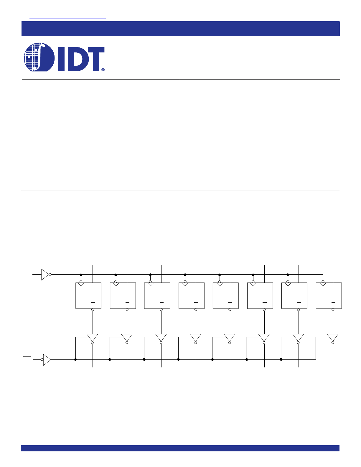
FUNCTIONAL BLOCK DIAGRAM
IDT54/74FCT574/A/C
DESCRIPTION:
The FCT574 is an 8-bit register built using an advanced dual metal CMOS
technology. These registers consist of eight D-type flip-flops with a buffered
common clock and buffered 3-state output control. When the output enable
(OE) is low, the eight outputs are enabled. When the OE input is high, the
outputs are in the high-impedance state.
Input data meeting the set-up and hold time requirements of the D inputs
is transferred to the O outputs on the low-to-high transition of the clock input.
The FCT574 has non-inverting outputs with respect to the data at the D
inputs.
CP
OE
D0
D
CP
Q
O0 O1
CP
D1
D2
D
Q
D
CP CP
Q
O2 O3
D3
D4
D
Q
D
CP CP
Q
O4 O5
D5
D6
D
Q
D
CP CP
Q
O6
D7
D
Q
O7
The IDT logo is a registered trademark of Integrated Device Technology, Inc.
JUNE 2002MILITARY AND COMMERCIAL TEMPERATURE RANGES
1
© 2002 Integrated Device Technology, Inc. DSC-5428/2
Page 2
IDT54/74FCT574/A/C
FAST CMOS OCTAL D REGISTERS (3-STATE)
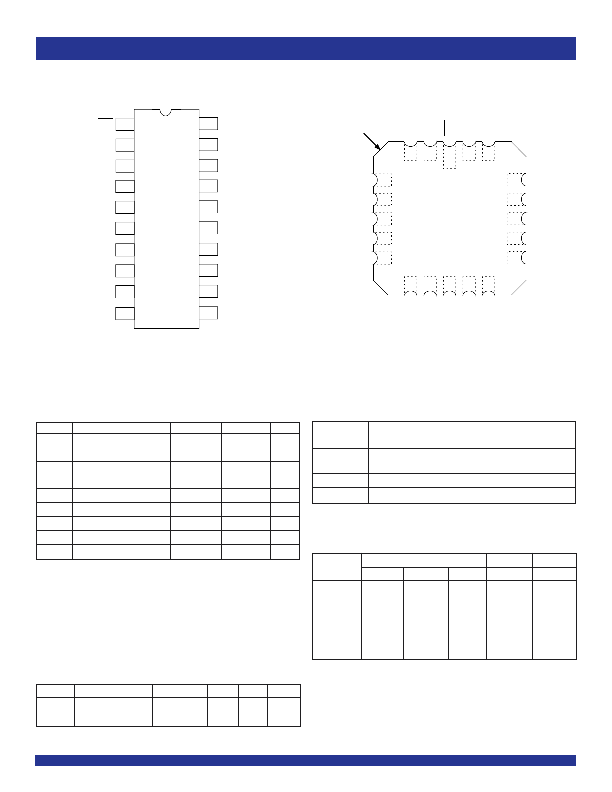
PIN CONFIGURATION
MILITARY AND COMMERCIAL TEMPERATURE RANGES
OE
D
D1
D2
D3
D4
D5
D6
D7
GND
1
0
2
3
4
5
6
7
8
9
10
20
19
18
17
16
15
14
13
12
11
VCC
O
0
O1
O2
O3
O4
O5
O6
O7
CP
CERDIP/ SOIC
TOP VIEW
ABSOLUTE MAXIMUM RATINGS
Symbol Rating Commercial Military Unit
(2)
V
TERM
V
TERM
TA Operating Temperature 0 to +70 –55 to +125 °C
TBIAS Temperature under BIAS –55 to +125 –65 to +135 °C
TSTG Storage Temperature –55 to +125 –65 to +150 °C
PT Power Dissipation 0.5 0.5 W
I
OUT DC Output Current 120 120 mA
NOTES:
1. Stresses greater than those listed under ABSOLUTE MAXIMUM RATINGS may cause
permanent damage to the device. This is a stress rating only and functional operation
of the device at these or any other conditions above those indicated in the operational
sections of this specification is not implied. Exposure to absolute maximum rating
conditions for extended periods may affect reliability. No terminal voltage may exceed
Vcc by +0.5V unless otherwise noted.
2. Input and Vcc terminals only.
3. Output and I/O terminals only.
Terminal Voltage –0.5 to +7 –0.5 to +7 V
with Respect to GND
(3)
Terminal Voltage –0.5 to VCC –0.5 to VCC V
with Respect to GND
(1)
CAPACITANCE (TA = +25°C, F = 1.0MHz)
Symbol Parameter
CIN Input Capacitance VIN = 0V 6 10 pF
C
OUT Output Capacitance VOUT = 0V 8 12 pF
NOTE:
1. This parameter is measured at characterization but not tested.
(1)
Conditions Typ. Max. Unit
INDEX
D2
D3
D4
D5
D6
E
0
D1D
4
5
6
7
8
9
7
D
O
23
1
10 11 12 13
P
D
C
N
C
V
7
O
0
O
1920
18
17
16
15
14
6
O1
O2
O3
O4
O5
O
C
G
LCC
TOP VIEW
PIN DESCRIPTION
Pin Names Description
Dx D flip-flop data inputs
CP Clock Pulse for the register. Enters data on LOW-to-
HIGH transition.
Ox 3-State Outputs (TRUE)
OE Active LOW 3-State Output Enable Input
FUNCTION TABLE
Function OE CP Dx Ox Ox
High-Z H L X Z NC
HHXZNC
Load L ↑ LLH
Register L ↑ HHL
H ↑ LZH
H ↑ HZL
NOTE:
1. H = HIGH Voltage Level
X = Don’t Care
L = LOW Voltage Level
Z = High Impedance
NC = No Change
↑ = LOW-to-HIGH transition
2
(1)
Inputs Outputs Internal
Page 3
IDT54/74FCT574/A/C
FAST CMOS OCTAL D REGISTERS (3-STATE)
MILITARY AND COMMERCIAL TEMPERATURE RANGES
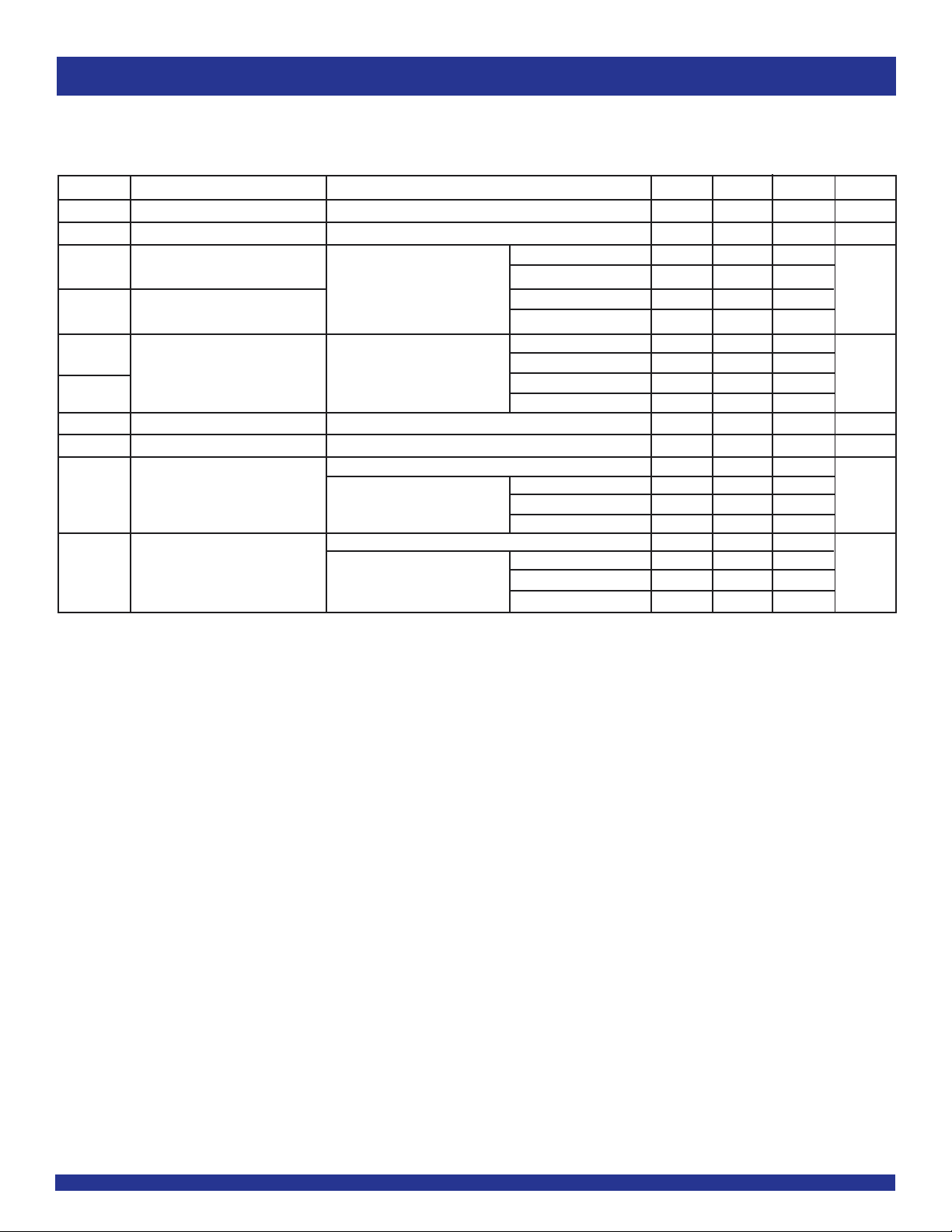
DC ELECTRICAL CHARACTERISTICS OVER OPERATING RANGE
Following Conditions Apply Unless Otherwise Specified: VLC = 0.2V; VHC = VCC - 0.2V
Commercial: TA = 0°C to +70°C, VCC = 5.0V ±5%, Military: TA = -55°C to +125°C, VCC = 5.0V ±10%
Symbol Parameter Test Conditions
(1)
Min. Typ.
VIH Input HIGH Level Guaranteed Logic HIGH Level 2 — — V
VIL Input LOW Level Guaranteed Logic LOW Level — — 0.8 V
IIH Input HIGH Current VI = VCC —— 5
CC = Max. VI = 2.7V — — 5
V
I
IL Input LOW Current VI = 0.5V — — –5
VI = GND — — –5
IOZH VO = VCC —— 10
Off State (High Impedance) V
OZL Output Current VO = 0.5V — — –10
I
CC = Max. VO = 2.7V — — 10
VO = GND — — –10
VIK Clamp Diode Voltage VCC = Min., IIN = –18mA — –0.7 –1.2 V
IOS Short Circuit Current VCC = Max., VO = GND
V
OH Output HIGH Voltage VCC = 3V, VIN = VLC or VHC, IOH = –32µAVHC VCC —
(3)
–60 –120 — mA
VCC = Min IOH = –300µAVHC VCC —V
VIN = VIH or VIL IOH = –12mA MIL 2.4 4.3 —
IOH = –15mA COM'L 2.4 4.3 —
VOL Output LOW Voltage VCC = 3V, VIN = VLC or VHC, IOL = 300µA — GND VLC
VCC = Min IOL = 300µA — GND VLC
VIN = VIH or VIL IOL = 32mA MIL — 0.3 0.5
IOL = 48mA COM'L — 0.3 0.5
NOTES:
1. For conditions shown as Min. or Max., use appropriate value specified under Electrical Characteristics for the applicable device type.
2. Typical values are at VCC = 5.0V, +25°C ambient and maximum loading.
3. Not more than one output should be tested at one time. Duration of the test should not exceed one second.
4. This parameter is guaranteed but not ttested.
(2)
Max. Unit
(4)
µA
(4)
(4)
(4)
(4)
µA
V
3
Page 4
IDT54/74FCT574/A/C
FAST CMOS OCTAL D REGISTERS (3-STATE)
MILITARY AND COMMERCIAL TEMPERATURE RANGES
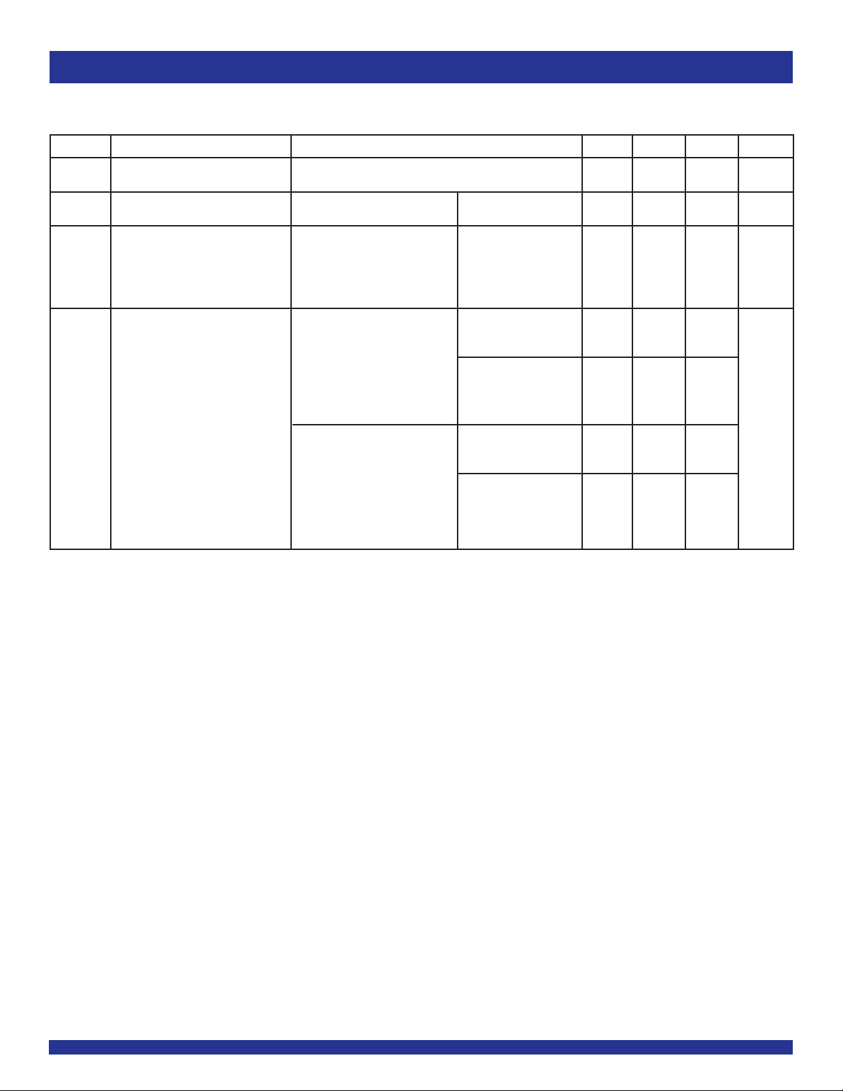
POWER SUPPLY CHARACTERISTICS
VLC = 0.2V; VHC = VCC - 0.2V
Symbol Parameter Test Conditions
CC Quiescent Power Supply Current VCC = Max. — 0.2 1.5 m A
I
(1)
Min. Typ.
VIN ≥ VHC; VIN ≤ VLC
∆ICC Quiescent Power Supply Current VCC = Max. — 0.5 2 mA
TTL Inputs HIGH VIN = 3.4V
(3)
ICCD Dynamic Power Supply VCC = Max. VIN ≥ VHC — 0.15 0.25 mA/
(4)
Current
Outputs Open VIN ≤ VLC MHz
OE = GND
One Input Toggling
50% Duty Cycle
I
C Total Power Supply Current
(6)
VCC = Max. VIN ≥ VHC — 1.7 4 mA
Outputs Open VIN ≤ VLC
fCP = 10MHz (FCT)
50% Duty Cycle V
IN = 3.4V — 2.2 6
OE = GND VIN = GND
fi = 5MHz
One Bit Toggling
V
CC = Max. VIN ≥ VHC — 4 7.8
Outputs Open VIN ≤ VLC
fCP = 10MHz (FCT)
50% Duty Cycle V
IN = 3.4V — 6.2 16.8
OE = GND VIN = GND
fi = 2.5MHz
Eight Bits Toggling
(2)
Max. Unit
(5)
(5)
NOTES:
1. For conditions shown as Min. or Max., use appropriate value specified under Electrical Characteristics for the applicable device type.
2. Typical values are at VCC = 5.0V, +25°C ambient.
3. Per TTL driven input (VIN = 3.4V). All other inputs at VCC or GND.
4. This parameter is not directly testable, but is derived for use in Total Power Supply Calculations.
5. Values for these conditions are examples of ∆ICC formula. These limits are guaranteed but not tested.
6. IC = IQUIESCENT + IINPUTS + IDYNAMIC
IC = ICC + ∆ICC DHNT + ICCD (fCP/2 + fiNi)
ICC = Quiescent Current
∆ICC = Power Supply Current for a TTL High Input (VIN = 3.4V)
DH = Duty Cycle for TTL Inputs High
NT = Number of TTL Inputs at DH
ICCD = Dynamic Current caused by an Input Transition Pair (HLH or LHL)
fCP = Clock Frequency for register devices (zero for non-register devices)
fi = Input Frequency
Ni = Number of Inputs at fi
All currents are in milliamps and all frequencies are in megahertz.
4
Page 5
IDT54/74FCT574/A/C
FAST CMOS OCTAL D REGISTERS (3-STATE)
MILITARY AND COMMERCIAL TEMPERATURE RANGES
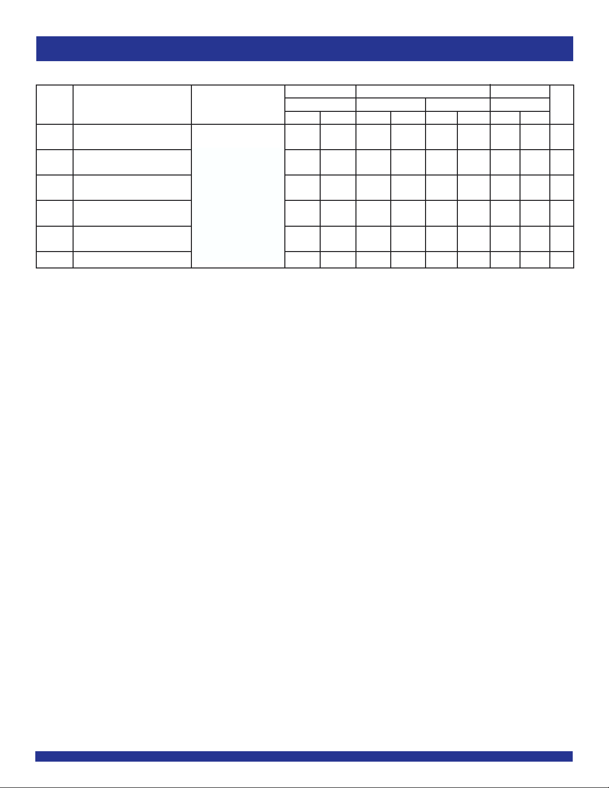
SWITCHING CHARACTERISTICS OVER OPERATING RANGE
54FCT574 54/74FCT574A 74FCT574C
Symbol Parameter Condition
PLH Propagation Delay CL = 50pF 2 11 2 6.5 2 7.2 2 5.2 ns
t
(1)
tPHL CP to Qx RL = 500Ω
PZH Output Enable Time 1.5 14 1.5 6 .5 1.5 7.5 1.5 5.5 ns
t
tPZL
tPHZ Output Disable Time 1.5 8 1.5 5. 5 1.5 6.5 1.5 5 ns
tPLZ
tSU Set-up Time HIGH or LOW 2 — 2 — 2 — 2 — ns
Dx to CP
H Hold Time HIGH or LOW 1.5 — 1.5 — 1.5 — 1.5 — ns
t
Dx to CP
t
W CP Pulse Width HIGH or LOW
NOTES:
1. See test circuit and waveforms.
2. Minimum limits are guaranteed but not tested on Propagation Delays.
3. This parameter is guaranteed but not tested.
(3)
Mil. Com'l. Mil. Com'l.
Min.
(2)
Max. Min.
(2)
Max. Min.
(2)
Max. Min.
(2)
Max. Unit
7— 5—6—5—ns
5
Page 6
IDT54/74FCT574/A/C
FAST CMOS OCTAL D REGISTERS (3-STATE)
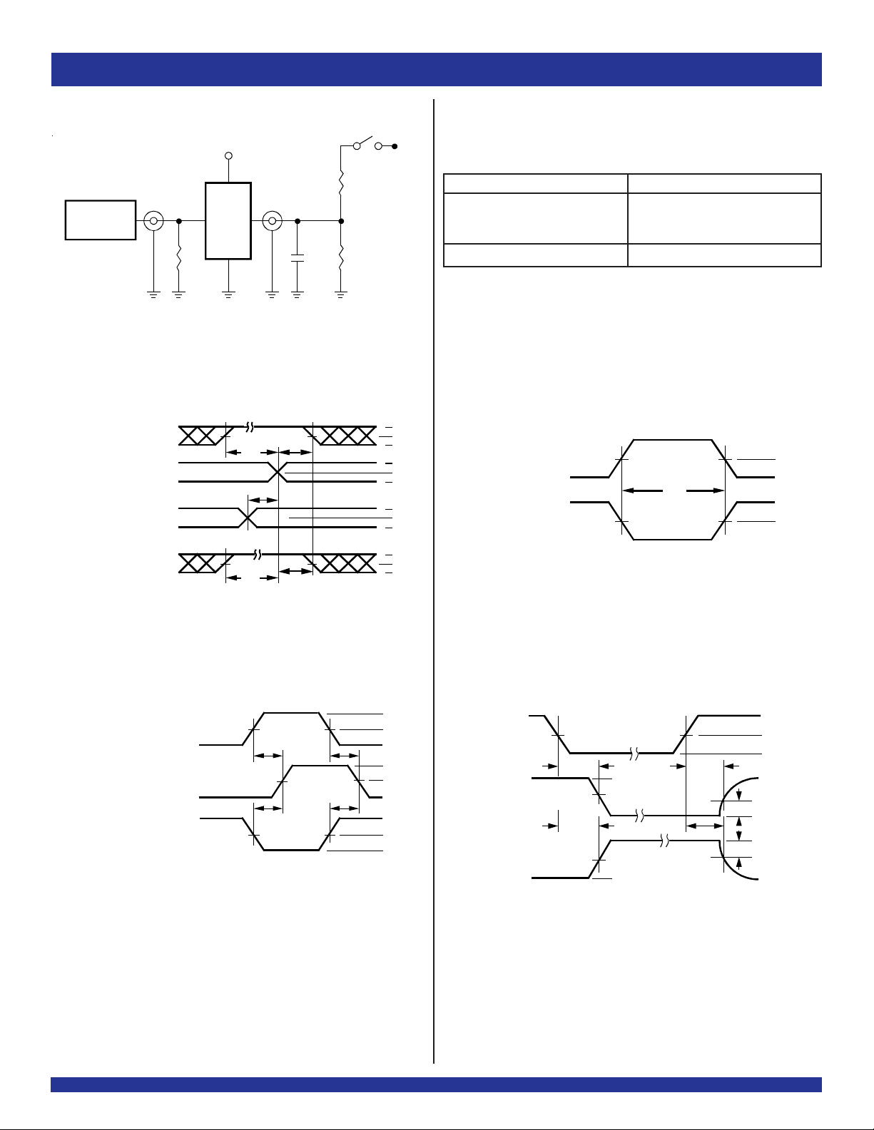
TEST CIRCUITS AND WAVEFORMS
MILITARY AND COMMERCIAL TEMPERATURE RANGES
IN
Pulse
Generator
V
D.U.T
.
T
R
Test Circuits for All Outputs
DATA
INPUT
TIMING
INPUT
ASYNCHRONOUS CONTROL
SYNCHRONOUS CONTROL
CLOCK ENABLE
PRESET
CLEAR
ETC.
PRESET
CLEAR
ETC.
VCC
tSU
tSU
VOUT
tREM
tH
50pF
L
C
tH
Octal link
500Ω
500Ω
Octal link
7.0V
3V
1.5V
0V
3V
1.5V
0V
3V
1.5V
0V
3V
1.5V
0V
SWITCH POSITION
Test Switch
Open Drain
Disable Low Closed
Enable Low
All Other Tests Open
DEFINITIONS:
L = Load capacitance: includes jig and probe capacitance.
C
R
T = Termination resistance: should be equal to ZOUT of the Pulse Generator.
LOW-HIGH-LOW
HIGH-LOW-HIGH
PULSE
tW
PULSE
Octal link
Pulse Width
1.5V
1.5V
Set-Up, Hold, and Release Times
SAME PHASE
INPUT TRANSITION
OUTPUT
OPPOSITE PHASE
INPUT TRANSITION
tPLH
tPLH tPHL
Propagation Delay
tPHL
Octal link
3V
1.5V
0V
OH
V
1.5V
VOL
3V
1.5V
0V
ENABLE DISABLE
3V
CONTROL
INPUT
OUTPUT
NORMALLY
LOW
SWITCH
CLOSED
tPLZtPZL
3.5V
1.5V
0.3V
1.5V
0V
3.5V
VOL
tPZH tPHZ
OUTPUT
NORMALLY
HIGH
SWITCH
OPEN
1.5V
0V
0.3V
VOH
0V
Octal link
Enable and Disable Times
NOTES:
1. Diagram shown for input Control Enable-LOW and input Control Disable-HIGH.
2. Pulse Generator for All Pulses: Rate ≤ 1.0MHz; ZO ≤ 50Ω; tF ≤ 2.5ns; tR ≤ 2.5ns.
6
Page 7
IDT54/74FCT574/A/C
FAST CMOS OCTAL D REGISTERS (3-STATE)
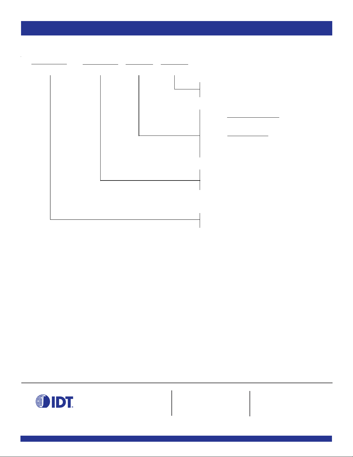
ORDERING INFORMATION
MILITARY AND COMMERCIAL TEMPERATURE RANGES
IDT XX
Temp. Range
FCT
Device Type
XXXX
XX
Package
X
Process
BlankBCommercial
MIL-STD-883, Class B
Commercial Options
SO
Small Outline IC
Military Options
D
L
574
CERDIP
Leadless Chip Carrier
Fast CMOS Octal D Register (3-State)
574A
574C
54
74
– 55°C to +125°C
0°C to +70°C
CORPORATE HEADQUARTERS for SALES: for Tech Support:
2975 Stender Way 800-345-7015 or 408-727-6116 [email protected]
Santa Clara, CA 95054 fax: 408-492-8674 (408) 654-6459
www.idt.com
7
 Loading...