

Datasheet IDT74FCT3573SO, IDT74FCT3573PYB, IDT74FCT3573PY, IDT74FCT3573PB, IDT74FCT3573P Datasheet (Integrated Device Technology)
...Page 1
Integrated Device Technology, Inc.
3.3V CMOS OCTAL
TRANSPARENT
LATCHES
IDT54/74FCT3573/A
ADVANCE INFORMATION
FEATURES:
• 0.5 MICRON CMOS Technology
• ESD > 2000V per MIL-STD-883, Method 3015;
> 200V using machine model (C = 200pF, R = 0)
• 25 mil Center SSOP Packages
• Extended commercial range of -40°C to +85°C
•V
CC = 3.3V ±0.3V, Normal Range or
VCC = 2.7V to 3.6V, Extended Range
• CMOS power levels (0.4µW typ. static)
• Rail-to-Rail output swing for increased noise margin
• Military product compliant to MIL-STD-883, Class B
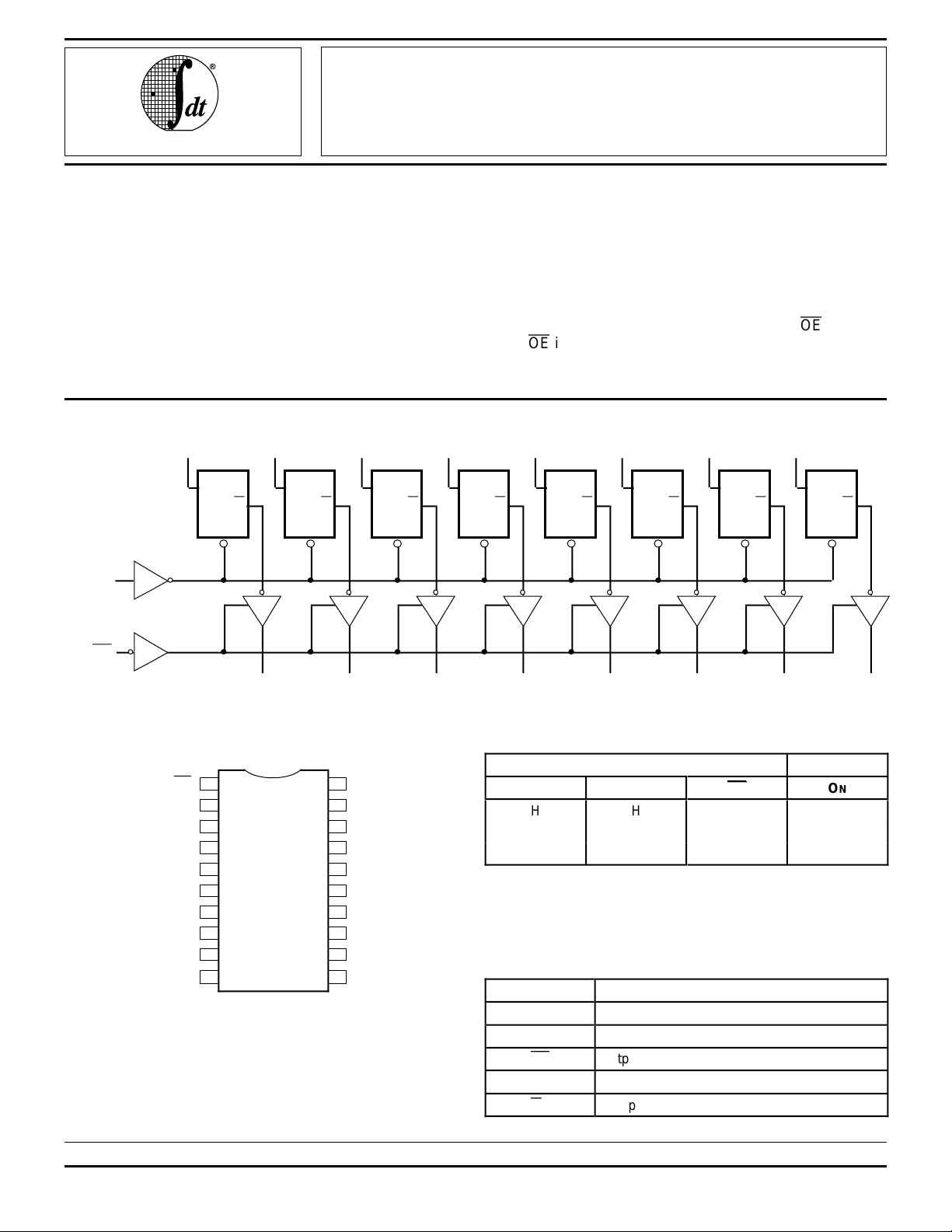
FUNCTIONAL BLOCK DIAGRAM
D0
D
G
LE
D1
D
O
G
D2
D
O
O
G
DESCRIPTION:
The FCT3573/A are octal transparent latches built using an
advanced dual metal CMOS technology.
These octal latches have 3-state outputs and are intended
for bus oriented applications. The flip-flops appear transparent to the data when Latch Enable (LE) is HIGH. When LE is
LOW, the data that meets the set-up time is latched. Data
appears on the bus when the Output Enable (OE) is LOW.
When OE is HIGH, the bus output is in the high-impedance
state.
D3
D
G
D4
D
O
G
D5
D
O
G
D6
D
O
G
D7
O
D
O
G
OE
O
0
PIN CONFIGURATION FUNCTION TABLE
OE
D0
D1
D2
D3
D4
D5
D6
D7
GND
The IDT logo is a registered trademark of Integrated Device Technology, Inc.
2
3
P20-1
4
D20-1
SO20-2
5
&
6
SO20-7
7
8
9
10 11
DIP/SOIC/SSOP
TOP VIEW
20
19
18
17
16
15
14
13
12
O
1
O
2
O
3
O
4
O
5
O
6
O
3093 drw 01
(1)
VCC1
O
O1
O2
O3
O4
O
O6
O7
LE
0
5
3093 drw 02
DN LE
HHLH
LHLL
XXHZ
NOTE:
1. H = HIGH Voltage Level
X = Don’t Care
L = LOW Voltage Level
Z = High Impedance
DEFINITION OF FUNCTIONAL TERMS
Pin Names Description
DN Data Inputs
LE Latch Enable Input (Active HIGH)
OE
ON 3-State Outputs
O
N Complementary 3-State Outputs
Inputs Outputs
OE
OE
Output Enable Input (Active LOW)
ON
3093 tbl 02
3093 tbl 03
MILITARY AND COMMERCIAL TEMPERATURE RANGES AUGUST 1995
1995 Integrated Device Technology, Inc. 8.13 DSC-4648/-
1
7
Page 2
IDT54/74FCT3573/3573A
3.3V CMOS OCTAL TRANSPARENT LATCHES MILITARY AND COMMERCIAL TEMPERATURE RANGES
ABSOLUTE MAXIMUM RATINGS
(1)
Symbol Rating Commercial Military Unit
(2)
VTERM
Terminal Voltage
–0.5 to +4.6 –0.5 to +4.6 V
with Respect to
GND
(3)
VTERM
Terminal Voltage
–0.5 to +7.0 –0.5 to +7.0 V
with Respect to
GND
(4)
VTERM
Terminal Voltage
with Respect to
GND
TA Operating
–0.5 to
CC + 0.5
V
–40 to +85 –55 to +125 °C
–0.5 to
VCC + 0.5
V
Temperature
TBIAS Temperature
–55 to +125 –65 to +135 °C
Under Bias
TSTG Storage
–55 to +125 –65 to +150 °C
Temperature
PT Power Dissipation 1.0 1.0 W
IOUT DC Output
–60 to +60 –60 to +60 mA
Current
NOTES:
1. Stresses greater than those listed under ABSOLUTE MAXIMUM RATINGS may cause permanent damage to the device. This is a stress rating
only and functional operation of the device at these or any other conditions
above those indicated in the operational sections of this specification is
not implied. Exposure to absolute maximum rating conditions for extended periods may affect reliability.
2. Vcc terminals.
3. Input terminals.
4. Output and I/O terminals.
3093 lnk 03
CAPACITANCE (TA = +25°C, f = 1.0MHz)
Symbol Parameter
CIN Input
Capacitance
COUT Output
Capacitance
NOTE:
1. This parameter is measured at characterization but not tested.
(1)
Conditions Typ. Max. Unit
VIN = 0V 3.5 6.0 pF
VOUT = 0V 4.0 8.0 pF
3093 lnk 04
8.13 2
Page 3
IDT54/74FCT3573/3573A
3.3V CMOS OCTAL TRANSPARENT LATCHES MILITARY AND COMMERCIAL TEMPERATURE RANGES
DC ELECTRICAL CHARACTERISTICS OVER OPERATING RANGE
Following Conditions Apply Unless Otherwise Specified:
Commercial: TA = –40°C to +85°C, VCC = 2.7V to 3.6V; Military: TA = –55°C to +125°C, VCC = 2.7V to 3.6V
Symbol Parameter Test Conditions
(1)
Min. Typ.
VIH Input HIGH Level (Input pins) Guaranteed Logic HIGH Level 2.0 — 5.5 V
Input HIGH Level (I/O pins) 2.0 — VCC+0.5
VIL Input LOW Level Guaranteed Logic LOW Level –0.5 — 0.8 V
(Input and I/O pins)
(6)
(6)
(6)
VCC = Max. VI = 5.5V — — ±1 µA
VI = VCC — — ±1
(6)
VI = GND — — ±1
VI = GND — — ±1
II H Input HIGH Current (Input pins)
Input HIGH Current (I/O pins)
II L Input LOW Current (Input pins)
Input LOW Current (I/O pins)
IOZH High Impedance Output Current VCC = Max. VO = VCC — — ±1 µA
IOZL (3-State Output pins)
(6)
VO = GND — — ±1
VIK Clamp Diode Voltage VCC = Min., IIN = –18mA — –0.7 –1.2 V
IODH Output HIGH Current VCC = 3.3V, VIN = VIH or VIL, VO = 1.5V
IODL Output LOW Current VCC = 3.3V, VIN = VIH or VIL, VO = 1.5V
(3)
(3)
–36 –60 –110 mA
50 90 200 mA
VOH Output HIGH Voltage VCC = Min. IOH = –0.1mA VCC–0.2 — — V
VIN = VIH or VIL IOH = –3mA 2.4 3.0 —
(5)
VCC = 3.0V
IN = VIH or VIL
V
IOH = –6mA MIL.
OH = –8mA COM'L.
I
2.4
VOL Output LOW Voltage VCC = Min. IOL = 0.1mA — — 0.2 V
VIN = VIH or VIL IOL = 16mA — 0.2 0.4
IOL = 24mA — 0.3 0.55
IOS Short Circuit Current
(4)
VCC = 3.0V
IN = VIH or VIL
V
VCC = Max., VO = GND
IOL = 24mA — 0.3 0.50
(3)
–60 –135 –240 mA
VH Input Hysteresis — — 150 — mV
ICCL
ICCH
Quiescent Power Supply Current VCC = Max.,
IN = GND or VCC
V
COM'L. — 0.1 10 µA
ICCZ MIL. — 0.1 100
NOTES:
1. For conditions shown as Max. or Min., use appropriate value specified under Electrical Characteristics for the applicable device type.
2. Typical values are at Vcc = 3.3V, +25°C ambient.
3. Not more than one output should be tested at one time. Duration of the test should not exceed one second.
4. This parameter is guaranteed but not tested.
5. V
OH = VCC –0.6V at rated current.
6. The test limits for this parameter is ± 5µA at T
A = –55°C.
(2)
Max. Unit
3.0 —
3093 lnk 05
8.13 3
Page 4

IDT54/74FCT3573/3573A
3.3V CMOS OCTAL TRANSPARENT LATCHES MILITARY AND COMMERCIAL TEMPERATURE RANGES
POWER SUPPLY CHARACTERISTICS
Symbol Parameter Test Conditions
∆ICC Quiescent Power Supply Current VCC = Max. VIN = VCC – 0.6V
ICCD Dynamic Power Supply
(4)
Current
VCC = Max.
Outputs Open
OE
= GND
(1)
V
IN = VCC
V
IN = GND
Min. Typ.
(3)
One Input Toggling
50% Duty Cycle
IC Total Power Supply Current
(6)
VCC = Max. VIN = VCC mA
Outputs Open VIN = GND
fi =10MHz
50% Duty Cycle VIN = VCC –0.6V
OE
= GND
V
IN = GND
LE = VCC
One Bit Toggling
VCC = Max.
Outputs Open
V
IN = VCC
V
IN = GND
fi = 2.5MHz
50% Duty Cycle
OE
= GND
LE = V
CC
V
IN = VCC –0.6V
V
IN = GND
Eight Bits Toggling
NOTES:
1. For conditions shown as max. or min., use appropriate value specified under Electrical Characteristics for the applicable device type.
2. Typical values are at V
3. Per TTL driven input; all other inputs at V
4. This parameter is not directly testable, but is derived for use in Total Power Supply Calculations.
5. Values for these conditions are examples of the I
C = IQUIESCENT + IINPUTS + IDYNAMIC
6. I
IC = ICC + ∆ICC DHNT + ICCD (fCPNCP/2 + fiNi)
CC = Quiescent Current (ICCL, ICCH and ICCZ)
I
∆I
CC = Power Supply Current for a TTL High Input
H = Duty Cycle for TTL Inputs High
D
T = Number of TTL Inputs at DH
N
ICCD = Dynamic Current Caused by an Input Transition Pair (HLH or LHL)
f
CP = Clock Frequency for Register Devices (Zero for Non-Register Devices)
CP = Number of Clock Inputs at fCP
N
fi = Input Frequency
i = Number of Inputs at fi
N
CC = 3.3V, +25°C ambient.
CC or GND.
CC formula. These limits are guaranteed but not tested.
(2)
Max. Unit
µA
µA/
MHz
3093 tbl 06
8.13 4
Page 5

IDT54/74FCT3573/3573A
3.3V CMOS OCTAL TRANSPARENT LATCHES MILITARY AND COMMERCIAL TEMPERATURE RANGES
SWITCHING CHARACTERISTICS OVER OPERATING RANGE
FCT3573 FCT3573A
Com'l. Mil. Com'l. Mil.
Symbol Parameter Conditions
tPLH
tPHL
tPLH
tPHL
tPZH
Propagation Delay
D
N to ON
CL = 50pF
R
L = 500Ω
Propagation Delay
LE to O
N
Output Enable Time 1.5 12.0 1.5 13.5 1.5 6.5 1.5 7.5 ns
(1)
tPZL
tPHZ
Output Disable Time 1.5 7.5 1.5 10.0 1.5 5.5 1.5 6.5 ns
tPLZ
tSU Set-up Time HIGH
or LOW, D
N to LE
tH Hold Time HIGH
or LOW, D
N to LE
tW LE Pulse Width
HIGH
NOTES:
1. See test circuit and waveforms.
2. Minimum limits are guaranteed but not tested on Propagation Delays.
3. Propagation Delays and Enable/Disable times are with V
and Enable/Disable times should be degraded by 20%.
CC = 3.3V ±0.3V, Normal Range. For VCC = 2.7V to 3.6V, Extended Range, all Propagation Delays
(2)
Min.
Max. Min.
1.5 8.0 1.5 8.5 1.5 5.2 1.5 5.6 ns
2.0 13.0 2.0 15.0 2.0 8.5 2.0 9.8 ns
2.0 — 2.0 — 2.0 — 2.0 — ns
1.5 — 1.5 — 1.5 — 1.5 — ns
6.0 — 6.0 — 5.0 — 6.0 — ns
(3)
(2)
Max. Min.
(2)
Max. Min.
(2)
Max. Unit
3093 tbl 07
8.13 5
Page 6

IDT54/74FCT3573/3573A
3.3V CMOS OCTAL TRANSPARENT LATCHES MILITARY AND COMMERCIAL TEMPERATURE RANGES
TEST CIRCUITS AND WAVEFORMS
TEST CIRCUITS FOR ALL OUTPUTS
V
CC
V
Pulse
Generator
V
IN
D.U.T.
R
T
OUT
50pF
C
L
500
500
←
Open
GND
Ω
Ω
3093 drw 03
SWITCH POSITION
6V
Open Drain
Disable Low
Enable Low
Disable High
Enable High
All Other tests Open
DEFINITIONS:
L= Load capacitance: includes jig and probe capacitance.
C
T = Termination resistance: should be equal to ZOUT of the Pulse
R
Generator.
Test Switch
SET-UP, HOLD AND RELEASE TIMES PULSE WIDTH
DATA
INPUT
TIMING
INPUT
ASYNCHRONOUS CONTROL
PRESET
CLEAR
ETC.
SYNCHRONOUS CONTROL
PRESET
CLEAR
CLOCK ENABLE
ETC.
t
t
REM
H
t
H
t
SU
t
SU
3V
1.5V
0V
3V
1.5V
0V
3V
1.5V
0V
3V
1.5V
0V
3093 drw 04
LOW-HIGH-LOW
PULSE
HIGH-LOW-HIGH
PULSE
6V
GND
3093 lnk 08
1.5V
t
W
1.5V
3093 drw 05
SAME PHASE
INPUT TRANSITION
OUTPUT
OPPOSITE PHASE
INPUT TRANSITION
t
PLH
t
PLH
t
PHL
t
PHL
3V
1.5V
0V
OH
V
1.5V
V
OL
3V
1.5V
0V
3093 drw 06
ENABLE AND DISABLE TIMESPROPAGATION DELAY
ENABLE DISABLE
3V
CONTROL
INPUT
t
t
PLZ
0.3V
PHZ
0.3V
F ≤ 2.5ns; tR ≤ 2.5ns.
t
PZL
OUTPUT
NORMALLY
OUTPUT
NORMALLY
HIGH
NOTES:
1. Diagram shown for input Control Enable-LOW and input Control DisableHIGH.
2. Pulse Generator for All Pulses: Rate ≤ 1.0MHz; t
CC is below 3V, input voltage swings should be adjusted not to exceed
3. If V
CC.
V
LOW
SWITCH
6V
t
PZH
SWITCH
GND
3V
1.5V
1.5V
0V
1.5V
0V
3V
V
OL
V
OH
0V
3093 drw 07
8.13 6
Page 7

IDT54/74FCT3573/3573A
3.3V CMOS OCTAL TRANSPARENT LATCHES MILITARY AND COMMERCIAL TEMPERATURE RANGES
ORDERING INFORMATION
IDT XX FCT
Temp. Range
X
Family
XX
Device TypeXPackage
X
Process
Blank
B
P
D
SO
PY
573
Commercial
MIL-STD-883, Class B
Plastic DIP (P20-1)
CERDIP (D20-1)
Small Outline IC (SO20-2)
Shrink Small Outline Package (SO20-7)
Non-Inverting Octal Transparent Latch
573A
3 3.3 Volt
54
74
–55°C to +125°C
–40°C to +85°C
3093 drw 08
8.13 7
 Loading...