

Datasheet IDT74FCT299CTD, IDT74FCT299CTSOB, IDT74FCT299CTSO, IDT74FCT299CTQB, IDT74FCT299CTQ Datasheet (Integrated Device Technology)
...Page 1
Integrated Device Technology, Inc.
FAST CMOS
8-INPUT UNIVERSAL
SHIFT REGISTER
IDT54/74FCT299T/AT/CT
FEATURES:
• Std., A and C speed grades
• Low input and output leakage ≤1µA (max.)
• CMOS power levels
• True TTL input and output compatibility
– V
OH = 3.3V (typ.)
– VOL = 0.3V (typ.)
• High drive outputs (-15mA IOH, 48mA IOL)
• Power off disable outputs permit “live insertion”
• Meets or exceeds JEDEC standard 18 specifications
• Product available in Radiation Tolerant and Radiation
Enhanced versions
• Military product compliant to MIL-STD-883, Class B
and DESC listed (dual marked)
• Available in DIP, SOIC, QSOP, CERPACK and LCC
packages
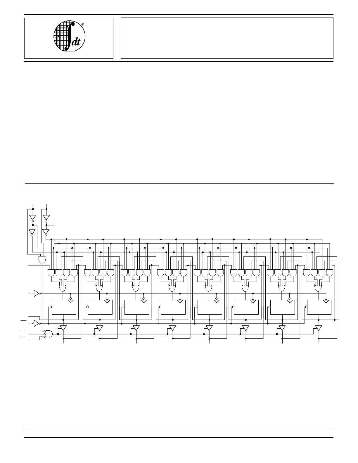
FUNCTIONAL BLOCK DIAGRAM
S1 S0
DESCRIPTION:
The IDT54/74FCT299T/AT/CT are built using an advanced
dual metal CMOS technology. The IDT54/74FCT299T/AT/
CT are 8-input universal shift/storage registers with 3-state
outputs. Four modes of operation are possible: hold (store),
shift left, shift right and load data. The parallel load inputs and
flip-flop outputs are multiplexed to reduce the total number of
package pins. Additional outputs are provided for flip-flops Q0
and Q7 to allow easy serial cascading. A separate active LOW
Master Reset is used to reset the register.
DS
0
CP
D
P
C
CD
0
Q
MR
OE1
OE2
The IDT logo is a registered trademark of Integrated Device Technology, Inc.
Q
CD
D
P
C
Q
CD
DS7
D
P
C
Q
CD
D
P
C
Q
CD
D
P
C
Q
CD
D
P
C
Q
D
P
C
CD
Q
I/O6I/O5I/O4I/O3I/O2I/O1I/O0 I/O7
CD
D
C
Q
2632 drw 01
P
Q7
MILITARY AND COMMERCIAL TEMPERATURE RANGES APRIL 1995
1995 Integrated Device Technology, Inc. 6.11 DSC-4205/4
1
Page 2
IDT54/74FCT299T/AT/CT
FAST CMOS 8-INPUT UNIVERSAL SHIFT REGISTER MILITARY AND COMMERCIAL TEMPERATURE RANGES
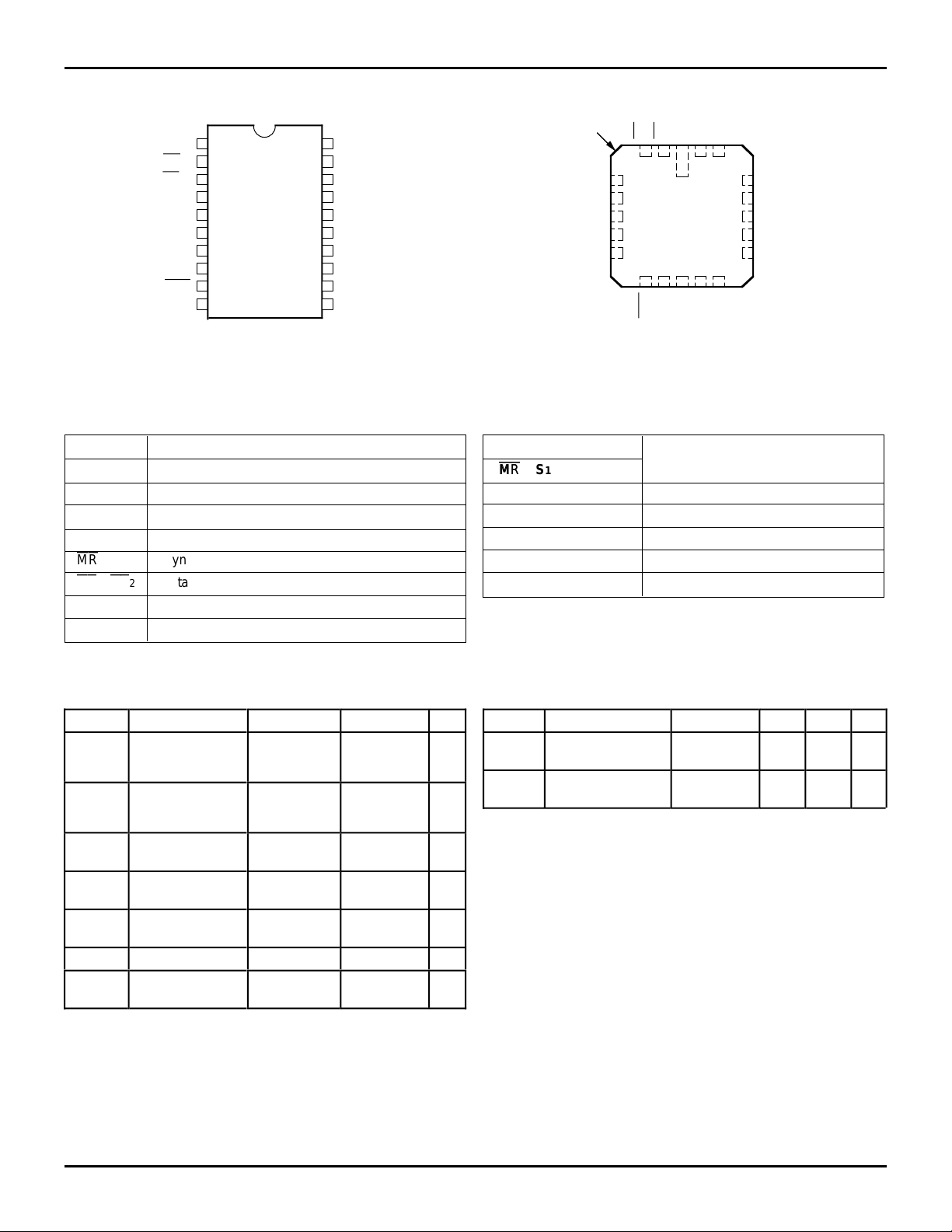
PIN CONFIGURATIONS
1
S0
Q0
2
3
4
5
6
7
8
9
10
P20-1
D20-1
SO20-2
SO20-8
E20-1
OE1
OE2
I/O6
I/O4
I/O2
I/O0
MR
GND
DIP/SOIC/QSOP/CERPACK
TOP VIEW
20
Vcc
19
S1
18
DS7
17
Q
7
16
I/O7
15
&
14
13
12
11
I/O5
I/O
I/O
CP
DS
2632 drw 02
PIN DESCRIPTION
Pin Names Description
CP Clock Pulse Input (Active Edge Rising)
0 Serial Data Input for Right Shift
DS
7 Serial Data Input for Left Shift
DS
0, S1 Mode Select Inputs
S
MR
1, OE2 3-State Output Enable Inputs (Active LOW)
OE
0–I/O7 Parallel Data Inputs or 3-State Parallel Outputs
I/O
0, O7 Serial Outputs
O
Asynchronous Master Reset Input (Active LOW)
2
INDEX
I/O
6
I/O
4
I/O
2
I/O
0
3
1
0
Q
0
OE
32
4
5
6
7
8
10 11 12 13
9
MR
1
OE
L20-2
GND
1
0
S
0
DS
Vcc
20 19
CP
1
S
18
17
16
15
14
1
I/O
2632 drw 03
DS
Q
I/O
I/O
I/O
7
7
7
5
3
LCC
TOP VIEW
(1)
0–Q7 = LOW
n → Qn
7 → Q7, Q7→ Q6, etc.
2632 tbl 01
FUNCTION TABLE
Inputs
1 S0 CP Response
MRMRS
L X X X Asynchronous Reset Q
HH H ↑Parallel Load; I/O
HL H ↑Shift Right; DS0 → Q0, Q0 → Q1, etc.
HH L ↑Shift Left; DS
H L L X Hold
NOTE: 2632 tbl 02
1. H = HIGH Voltage Level
L = LOW Voltage Level
X = Don’t Care
↑ = LOW-to-HIGH clock transition
ABSOLUTE MAXIMUM RATINGS
(1)
Symbol Rating Commercial Military Unit
(2)
VTERM
Terminal Voltage
–0.5 to +7.0 –0.5 to +7.0 V
with Respect to
GND
(3)
VTERM
TA Operating
Terminal Voltage
with Respect to
GND
–0.5 to
V
CC +0.5
–0.5 to
VCC +0.5
0 to +70 –55 to +125 °C
V
Temperature
TBIAS Temperature
–55 to +125 –65 to +135 °C
Under Bias
TSTG Storage
–55 to +125 –65 to +150 °C
Temperature
PT Power Dissipation 0.5 0.5 W
IOUT DC Output
–60 to +120 –60 to +120 mA
Current
NOTES:
1. Stresses greater than those listed under ABSOLUTE MAXIMUM RATINGS may cause permanent damage to the device. This is a stress rating
only and functional operation of the device at these or any other
conditions above those indicated in the operational sections of this
specification is not
conditions for extended periods may affect reliability. No terminal voltage
may exceed V
2. Input and V
3. Outputs and I/O terminals only.
implied. Exposure to absolute maximum rating
CC by +0.5V unless otherwise noted.
CC terminals only.
2632 lnk 03
CAPACITANCE (TA = +25°C, f = 1.0MHz)
Symbol Parameter
C
IN
Input
Capacitance
C
OUT
Output
Capacitance
NOTE:
1. This parameter is measured at characterization but not tested.
(1)
Conditions Typ. Max. Unit
VIN = 0V 6 10
V
OUT
= 0V 8 12
pF
pF
2632 lnk 04
6.11 2
Page 3
IDT54/74FCT299T/AT/CT
FAST CMOS 8-INPUT UNIVERSAL SHIFT REGISTER MILITARY AND COMMERCIAL TEMPERATURE RANGES
DC ELECTRICAL CHARACTERISTICS OVER OPERATING RANGE
Following Conditions Apply Unless Otherwise Specified:
Commercial: TA = 0°C to +70°C, VCC = 5.0V ± 5%; Military: TA = –55°C to +125°C, VCC = 5.0V ± 10%
Symbol Parameter Test Conditions
V
IH Input HIGH Level Guaranteed Logic HIGH Level 2.0 — — V
IL Input LOW Level Guaranteed Logic LOW Level — — 0.8 V
V
(4)
(4)
(4)
VCC = Max., VI = 2.7V — — ±1 µA
VCC = Max., VI = 0.5V — — ±1 µA
VCC = Max., VI = Vcc (Max.) — — ±1 µA
(3)
VO = GND –60 –120 –225 mA
IN = VIH or VIL IOH = –8mA COM'L.
V
IN = VIH or VIL IOL = 48mA COM'L.
V
IH Input HIGH Current
I
IL Input LOW Current
I
I Input HIGH Current
I
IK Clamp Diode Voltage VCC = Min., IN = –18mA — –0.7 –1.2 V
V
OS Short Circuit Current VCC = Max.,
I
OH Output HIGH Voltage VCC = Min. IOH = –6mA MIL. 2.4 3.3 — V
V
OL Output LOW Voltage VCC = Min. IOL = 32mA MIL. — 0.3 0.5 V
V
OFF Input/Output Power Off VCC = 0V, VIN or VO ≤ 4.5V — — ±1 µA
I
Leakage
(5)
(1)
OH = –12mA MIL. 2.0 3.0 — V
I
OH= –15mA COM'L.
I
Min. Typ.
VH Input Hysteresis — — 200 — mV
CC Quiescent Power VCC = Max. — 0.01 1 mA
I
Supply Current V
NOTES: 2632 tbl 05
1. For conditions shown as Max. or Min., use appropriate value specified under Electrical Characteristics for the applicable device type.
2. Typical values are at V
3. Not more than one output should be shorted at one time. Duration of the short circuit test should not exceed one second.
4. The test limit for this parameter is ±5µA at T
5. This parameter is guaranteed but not tested.
CC = 5.0V, +25°C ambient.
IN = GND or VCC
A = -55°C.
(2)
Max. Unit
6.11 3
Page 4

IDT54/74FCT299T/AT/CT
FAST CMOS 8-INPUT UNIVERSAL SHIFT REGISTER MILITARY AND COMMERCIAL TEMPERATURE RANGES
POWER SUPPLY CHARACTERISTICS
Symbol Parameter Test Conditions
CC Quiescent Power Supply Vcc = Max. — 0.5 2.0 mA
∆I
Current TTL Inputs HIGH V
ICCD Dynamic Power Supply Vcc = Max. VIN = VCC — 0.15 0.25 mA/MHz
Current
(4)
IN = 3.4V
Outputs Open VIN = GND
OE
MR
(3)
1 = OE2 = GND
= V
CC
(1)
Min. Typ.
S0 = S1 = VCC
DS0 = DS1 = GND
One Input Toggling
50% Duty Cycle
I
C Total Power Supply Vcc = Max. VIN = VCC — 1.5 3.5 mA
Current
(6)
Outputs Open VIN = GND
f
CP = 10MHz
50% Duty Cycle
OE
1 = OE2 = GND
MR
= V
CC
S0 = S1 = VCC
DS0 = DS7 = GND VIN = 3.4V — 2.0 5.5
One Bit Toggling V
at f
i = 5MHz
IN = GND
50% Duty Cycle
Vcc = Max. V
IN = VCC — 3.8 7.3
Outputs Open VIN = GND
f
CP = 10MHz
50% Duty Cycle
OE
1 = OE2 = GND
MR
= V
CC
S0 = S1 = VCC
DS0 = DS7 = GND VIN = 3.4V — 6.0 16.3
Eight Bits Toggling VIN = GND
at f
i = 2.5MHz
50% Duty Cycle
NOTES: 2632 tbl 06
1. For conditions shown as Max. or Min., use appropriate value specified under Electrical Characteristics for the applicable device type.
2. Typical values are at V
3. Per TTL driven input (V
4. This parameter is not directly testable, but is derived for use in Total Power Supply calculations.
5. Values for these conditions are examples of the I
C = IQUIESCENT + IINPUTS + IDYNAMIC
6. I
IC = ICC + ∆ICC DHNT + ICCD (fCP/2 + fiNi)
CC = Quiescent Current
I
CC = Power Supply Current for a TTL High Input (VIN = 3.4V)
∆I
H = Duty Cycle for TTL Inputs High
D
N
T = Number of TTL Inputs at DH
ICCD = Dynamic Current Caused by an Output Transition Pair (HLH or LHL)
CP = Clock Frequency for Register Devices (Zero for Non-Register Devices)
f
i = Input Frequency
f
N
i = Number of Inputs at fi
All currents are in milliamps and all frequencies are in megahertz.
CC = 5.0V, +25°C ambient.
IN = 3.4V); all other inputs at VCC or GND.
CC formula. These limits are guaranteed but not tested.
(2)
Max. Unit
(5)
(5)
6.11 4
Page 5

IDT54/74FCT299T/AT/CT
FAST CMOS 8-INPUT UNIVERSAL SHIFT REGISTER MILITARY AND COMMERCIAL TEMPERATURE RANGES
SWITCHING CHARACTERISTICS OVER OPERATING RANGE
IDT54/74FCT299T IDT54/74FCT299AT IDT54/74FCT299CT
Com’l. Mil. Com’l. Mil. Com’l. Mil.
Symbol Parameter Condition
PLH Propagation Delay CL = 50pF 2.0 10.0 2.0 14.0 2.0 7.2 2.0 9.5 2.0 6.5 2.0 7.5 ns
t
t
PHL CP to Q0 or Q7 RL = 500Ω
PLH Propagation Delay 2.0 12.0 2.0 12.0 2.0 7.2 2.0 9.5 2.0 6.5 2.0 7.5 ns
t
t
PHL CP to I/On
(1)
tPHL Propagation Delay 2.0 10.0 2.0 10.5 2.0 7.2 2.0 9.5 2.0 6.5 2.0 7.5 ns
MR
to Q
0 or Q7
tPHL Propagation Delay 2.0 15.0 2.0 15.0 2.0 8.7 2.0 11.5 2.0 6.5 2.0 7.5 ns
MR
to I/O
n
tPZH Output Enable Time 1.5 11.0 1.5 15.0 1.5 6.5 1.5 7.5 1.5 6.5 1.5 7.5 ns
t
PZL
OE
n to I/On
tPHZ Output Disable Time 1.5 7.0 1.5 9.0 1.5 6.0 1.5 6.5 1.5 6.0 1.5 6.5 ns
t
PLZ
OE
n to I/On
tSU Set-up Time HIGH 7.5 — 7.5 — 3.5 — 4.0 — 3.5 — 4.0 — ns
or LOW
S
0 or S1 to CP
SU Set-up Time HIGH 5.5 — 5.5 — 4.0 — 4.5 — 4.0 — 4.5 — ns
t
or LOW I/O
DS
0 or DS7 to CP
n,
tH Hold Time HIGH 1.0 — 1.0 — 1.0 — 1.0 — 1.0 — 1.0 — ns
or LOW
S
H Hold Time HIGH 1.5 — 1.5 — 1.5 — 1.5 — 1.5 — 1.5 — ns
t
DS
0 or S1 to CP
or LOW I/O
0 or DS7 to CP
n,
tW CP Pulse Width 7.0 — 7.0 — 5.0 — 6.0 — 5.0 — 6.0 — ns
HIGH or LOW
tw
MR
Pulse Width 7.0 — 7.0 — 5.0 — 6.0 — 5.0 — 6.0 — ns
LOW
t
REM Recovery Time 7.0 — 7.0 — 5.0 — 6.0 — 5.0 — 6.0 — ns
Min.
(2)
Max. Min.
(2)
Max. Min.
(2)
Max. Min.
(2)
Max. Min.
(2)
Max. Min.
(2)
Max. Unit
NOTES:
1. See test circuit and waveforms.
2. Minimum units are guaranteed but not tested on Propagation Delays.
2619 tbl 07
6.11 5
Page 6

IDT54/74FCT299T/AT/CT
FAST CMOS 8-INPUT UNIVERSAL SHIFT REGISTER MILITARY AND COMMERCIAL TEMPERATURE RANGES
TEST CIRCUITS AND WAVEFORMS
TEST CIRCUITS FOR ALL OUTPUTS
V
CC
SWITCH POSITION
7.0V
Test Switch
Open Drain
Disable Low
Enable Low
All Other Tests
Generator.
Pulse
Generator
500Ω
V
V
IN
OUT
D.U.T.
50pF
T
R
C L
500Ω
2632 drw 04
DEFINITIONS:
C
L= Load capacitance: includes jig and probe capacitance.
T = Termination resistance: should be equal to ZOUT of the Pulse
R
SET-UP, HOLD AND RELEASE TIMES PULSE WIDTH
DATA
INPUT
TIMING
INPUT
ASYNCHRONOUS CONTROL
PRESET
CLEAR
ETC.
SYNCHRONOUS CONTROL
PRESET
CLEAR
CLOCK ENABLE
ETC.
tSU
tSU
tH
tREM
tH
3V
1.5V
0V
3V
1.5V
0V
3V
1.5V
0V
3V
1.5V
0V
2632 drw 05
LOW-HIGH-LOW
PULSE
HIGH-LOW-HIGH
PULSE
Closed
Open
2632 lnk 08
1.5V
tW
1.5V
2632 drw 06
SAME PHASE
INPUT TRANSITION
OUTPUT
OPPOSITE PHASE
INPUT TRANSITION
tPLH
tPHL
tPLH tPHL
3V
1.5V
0V
OH
V
1.5V
VOL
3V
1.5V
0V
2632 drw 07
ENABLE AND DISABLE TIMESPROPAGATION DELAY
ENABLE DISABLE
3V
CONTROL
INPUT
PLZtPZL
t
OUTPUT
NORMALLY
LOW
SWITCH
CLOSED
3.5V
1.5V
tPZH tPHZ
OUTPUT
NORMALLY
HIGH
NOTES:
1. Diagram shown for input Control Enable-LOW and input Control DisableHIGH
2. Pulse Generator for All Pulses: Rate ≤ 1.0MHz; t
SWITCH
OPEN
1.5V
0V
F ≤ 2.5ns; tR ≤ 2.5ns
0.3V
0.3V
1.5V
0V
3.5V
VOL
VOH
0V
2632 drw 08
6.11 6
Page 7

IDT54/74FCT299T/AT/CT
FAST CMOS 8-INPUT UNIVERSAL SHIFT REGISTER MILITARY AND COMMERCIAL TEMPERATURE RANGES
ORDERING INFORMATION
IDT XX X
Temperature
FCT
Family
Range
XXXX
Device Type
X
Package
X
Process
Blank
B
P
D
SO
L
E
Q
299T
Commercial
MIL-STD-883, Class B
Plastic DIP
CERDIP
Small Outline IC
Leadless Chip Carrier
CERPACK
Quarter-size Small Outline Package
8-Input Universal Shift Register
299AT
299CT
Blank High Drive
54
74
–55°C to +125°C
°
C to +70°C
0
2632 drw 09
6.11 7
 Loading...