

Datasheet IDT74FCT16823ETEB, IDT74FCT16823ETE, IDT74FCT16823CTPVB, IDT74FCT16823CTPV, IDT74FCT16823CTPFB Datasheet (Integrated Device Technology)
...
Integrated Device Technology, Inc.
FAST CMOS 18-BIT
REGISTER
IDT54/74FCT16823AT/BT/CT/ET
IDT54/74FCT162823AT/BT/CT/ET
FEATURES:
• Common features:
– 0.5 MICRON CMOS Technology
– High-speed, low-power CMOS replacement for
ABT functions
– Typical tSK(o) (Output Skew) < 250ps
– Low input and output leakage ≤1µA (max.)
– ESD > 2000V per MIL-STD-883, Method 3015;
> 200V using machine model (C = 200pF, R = 0)
– Packages include 25 mil pitch SSOP, 19.6 mil pitch
TSSOP, 15.7 mil pitch TVSOP and 25 mil pitch Cerpack
– Extended commercial range of -40°C to +85°C
–V
CC = 5V ±10%
• Features for FCT16823AT/BT/CT/ET:
– High drive outputs (-32mA IOH, 64mA IOL)
– Power off disable outputs permit “live insertion”
– Typical VOLP (Output Ground Bounce) < 1.0V at
VCC = 5V, TA = 25°C
• Features for FCT162823AT/BT/CT/ET:
– Balanced Output Drivers: ±24mA (commercial),
±16mA (military)
– Reduced system switching noise
– Typical VOLP (Output Ground Bounce) < 0.6V at
VCC = 5V,TA = 25°C
DESCRIPTION:
The FCT16823AT/BT/CT/ET and FCT162823AT/BT/CT/
ET 18-bit bus interface registers are built using advanced,
dual metal CMOS technology. These high-speed, low-power
registers with clock enable (x
trols are ideal for parity bus interfacing in high-performance
synchronous systems. The control inputs are organized to
operate the device as two 9-bit registers or one 18-bit register.
Flow-through organization of signal pins simplifies layout. All
inputs are designed with hysteresis for improved noise margin.
The FCT16823AT/BT/CT/ET are ideally suited for driving
high-capacitance loads and low-impedance backplanes. The
output buffers are designed with power off disable capability
to allow "live insertion" of boards when used as backplane
drivers.
The FCT162823AT/BT/CT/ET have balanced output drive
with current limiting resistors. This offers low ground bounce,
minimal undershoot, and controlled output fall times – reducing the need for external series terminating resistors. The
FCT162823AT/BT/CT/ET are plug-in replacements for the
FCT16823AT/BT/CT/ET and ABT16823 for on-board interface applications.
CLKEN
) and clear (x
CLR
) con-
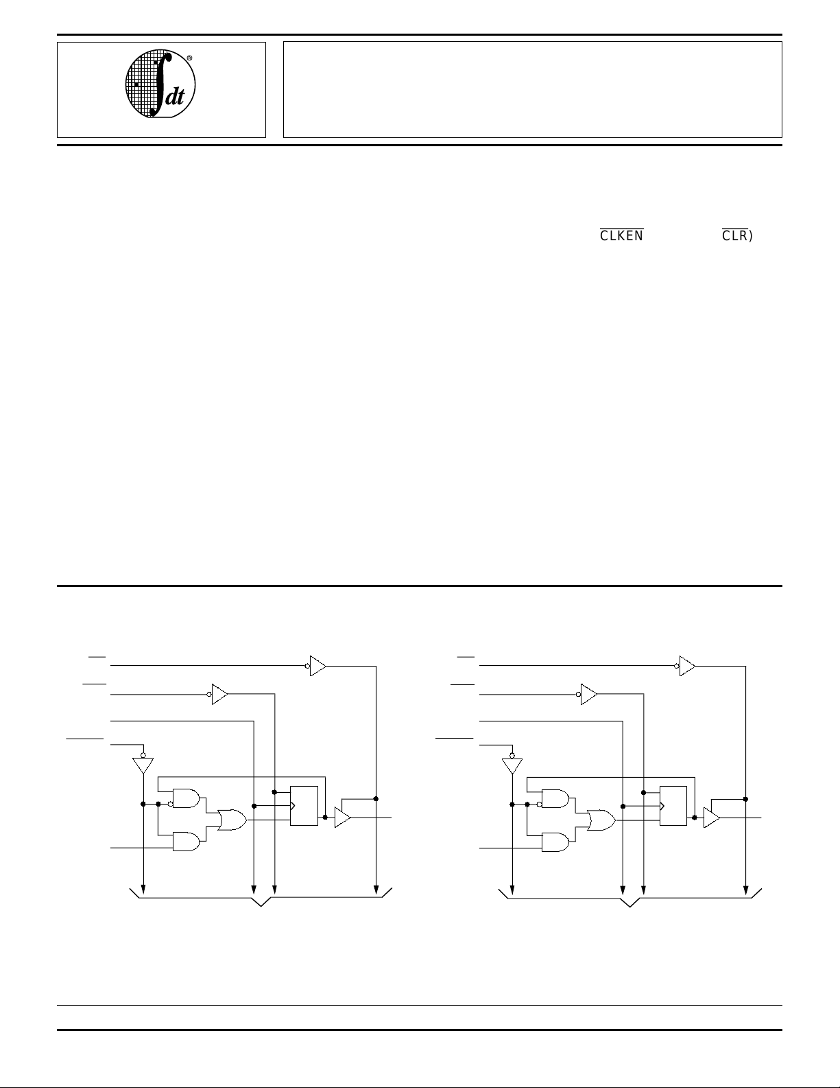
FUNCTIONAL BLOCK DIAGRAM
1OE
1CLR
1CLK
1CLKEN
R
C
D
1D1
TO 8 OTHER CHANNELS
The IDT logo is a registered trademark of Integrated Device Technology, Inc.
Q1
1
2772 drw 01 2772 drw 02
MILITARY AND COMMERCIAL TEMPERATURE RANGES AUGUST 1996
1996 Integrated Device Technology, Inc. 5.16 DSC-2772/8
2OE
2CLR
2CLK
2CLKEN
2D1
R
C
D
TO 8 OTHER CHANNELS
Q1
2
1
IDT54/74FCT16823AT/BT/CT/ET, 162823AT/BT/CT/ET
FAST CMOS 18-BIT REGISTER MILITARY AND COMMERCIAL TEMPERATURE RANGES
PIN CONFIGURATIONS
1
CLR
1
OE
1Q1
GND
1Q2
Q3
1
VCC
Q4
1
1
Q5
Q6
1
GND
Q7
1
1
Q8
1Q9
Q1
2
Q2
2
2
Q3
GND
2
Q4
Q5
2
2
Q6
V
CC
2Q7
2
Q8
GND
Q9
2
2
OE
2CLR
1
2
3
4
5
6
7
8
9
10
11
12
13
14
15
16
17
18
19
20
21
22
23
24
26
27
28
SO56-1
SO56-2
SO56-3
48
43
56
55
54
53
52
51
50
49
47
46
45
44
42
41
40
39
38
37
36
35
34
33
3225
31
30
29
1CLK
1
CLKEN
1D1
GND
1D2
1
D3
VCC
D4
1
D5
1
1
D6
GND
D7
1
1
D8
D9
1
2D1
2D2
2D3
GND
2D4
2
D5
D6
2
VCC
2D7
D8
2
GND
2
D9
CLKEN
2
CLK
2
CLR
1
1
OE
1
GND
1Q2
1
V
1
1
1
GND
1
1
1Q9
2
2
2
GND
2
2
2
V
2Q7
2
GND
2Q9
2
OE
2
CLR
Q
Q
Q
Q
Q
Q
Q
Q
Q
Q
Q
Q
Q
Q
CC
CC
1
2
1
3
4
5
3
6
7
4
5
6
8
9
10
11
7
8
1
2
3
12
13
14
15
16
17
E56-1
18
4
5
6
19
20
21
22
23
8
24
25
26
27
28
56
55
54
53
52
51
50
49
48
47
46
45
44
43
42
41
40
39
38
37
36
35
34
33
32
31
30
29
CLK
1
1
CLKEN
1D1
GND
1D2
1
D
3
V
CC
1
D
4
1
D
5
1
D
6
GND
1
D
7
1
D
8
1
D
9
2D1
2
D
2
2
D
3
GND
2D4
D
5
2
2
D
6
V
CC
2D7
D
8
2
GND
2
D
9
CLKEN
2
2
CLK
SSOP/
TSSOP/TVSOP
TOP VIEW
CERPACK
TOP VIEW
2772 drw 03 2772 drw 04
5.16 2
IDT54/74FCT16823AT/BT/CT/ET, 162823AT/BT/CT/ET
FAST CMOS 18-BIT REGISTER MILITARY AND COMMERCIAL TEMPERATURE RANGES
PIN DESCRIPTION
Pin Names Description
xDx Data inputs
xCLK Clock Inputs
x
CLKEN
x
CLR
x
OE
xQx 3-State Outputs
ABSOLUTE MAXIMUM RATINGS
Symbol Description Max. Unit
(2)
VTERM
VTERM
TSTG Storage Temperature –65 to +150 °C
IOUT DC Output Current –60 to +120 mA
NOTES:
1. Stresses greater than those listed under ABSOLUTE MAXIMUM RATINGS may cause permanent damage to the device. This is a stress rating
only and functional operation of the device at these or any other conditions
above those indicated in the operational sections of this specification is
not implied. Exposure to absolute maximum rating conditions for
extended periods may affect reliability.
2. All device terminals except FCT162XXXT Output and I/O terminals.
3. Output and I/O terminals for FCT162XXXT.
Terminal Voltage with Respect to
GND
(3)
Terminal Voltage with Respect to
GND
Clock Enable Inputs (Active LOW)
Asynchronous clear Inputs
(Active LOW)
Output Enable Inputs (Active LOW)
(1)
–0.5 to +7.0 V
–0.5 to
CC +0.5
V
2772 tbl 01
V
2772 lnk 03
FUNCTION TABLE
(1)
Inputs Outputs
x
OEOEx
CLR
CLR
x
CLKEN
CLKEN
xCLK xDx xQx Function
H X X X X Z High Z
L L X X X L Clear
LHHXXQ
(2)
Hold
HH L ↑L Z Load
HH L ↑HZ
LH L ↑LL
LH L ↑HH
NOTES: 2772 tbl 02
1. H = HIGH Voltage Level
L = LOW Voltage Level
X = Don’t Care
Z = High Impedance
2. Output level before indicated steady-state input conditions were established.
CAPACITANCE (TA = +25°C, f = 1.0MHz)
Symbol Parameter
CIN Input
Capacitance
COUT Output
Capacitance
NOTE:
1. This parameter is measured at characterization but not tested.
(1)
Conditions Typ. Max. Unit
VIN = 0V 3.5 6.0 pF
VOUT = 0V 3.5 8.0 pF
2772 lnk 04
5.16 3

IDT54/74FCT16823AT/BT/CT/ET, 162823AT/BT/CT/ET
FAST CMOS 18-BIT REGISTER MILITARY AND COMMERCIAL TEMPERATURE RANGES
DC ELECTRICAL CHARACTERISTICS OVER OPERATING RANGE
Following Conditions Apply Unless Otherwise Specified:
Commercial: T
Symbol Parameter Test Conditions
VIH Input HIGH Level Guaranteed Logic HIGH Level 2.0 — — V
VIL Input LOW Level Guaranteed Logic LOW Level — — 0.8 V
II H Input HIGH Current (Input pins)
II L Input LOW Current (Input pins)
IOZH High Impedance Output Current VCC = Max. VO = 2.7V — — ±1 µA
IOZL (3-State Output pins)
VIK Clamp Diode Voltage VCC = Min., IIN = –18mA — –0.7 –1.2 V
IOS Short Circuit Current VCC = Max., VO = GND
VH Input Hysteresis — — 100 — mV
ICCL
ICCH
ICCZ
A = –40°C to +85°C, VCC = 5.0V ± 10%; Military: TA = –55°C to +125°C, VCC
(1)
(5)
VCC = Max. VI = VCC — — ±1 µA
Input HIGH Current (I/O pins)
Input LOW Current (I/O pins)
(5)
(5)
(5)
VI = GND — — ±1
(5)
VO = 0.5V — — ±1
(3)
= 5.0V ± 10%
Min. Typ.
(2)
Max. Unit
— — ±1
— — ±1
–80 –140 –225 mA
Quiescent Power Supply Current VCC = Max., VIN = GND or VCC — 5 500 µA
2772 lnk 05
OUTPUT DRIVE CHARACTERISTICS FOR FCT16823T
Symbol Parameter Test Conditions
I
O
V
OH
Output Drive Current VCC = Max., VO = 2.5V
Output HIGH Voltage VCC = Min. IOH = –3mA 2.5 3.5 — V
VIN = V
IH
or V
IL
(3)
IOH = –12mA MIL.
I
OH
= –15mA COM'L.
IOH = –24mA MIL.
I
OH
= –32mA COM'L.
V
I
OFF
OL
Output LOW Voltage VCC = Min.
V
IN
= V
IH
VCC = 0V, V
Input/Output Power Off Leakage
(5)
or V
IN
I
OL
= 48mA MIL.
IL
or V
I
OL
= 64mA COM'L.
O
≤ 4.5V — —
(1)
Min. Typ.
–50
2.4 3.5 — V
2.0 3.0 — V
(4)
— 0.2 0.55 V
(2)
Max. Unit
—–
180 mA
±
1
µ
A
2772 lnk 06
OUTPUT DRIVE CHARACTERISTICS FOR FCT162823T
Symbol Parameter Test Conditions
IODL Output LOW Current VCC = 5V, VIN = VIH or VIL, VOUT = 1.5V
IODH Output HIGH Current VCC = 5V, VIN = VIH or V IL,
VOH Output HIGH Voltage VCC = Min.
V
IN = VIH or VIL
VOL Output LOW Voltage VCC = Min.
V
IN = VIH or VIL
NOTES:
1. For conditions shown as Max. or Min., use appropriate value specified under Electrical Characteristics for the applicable device type.
2. Typical values are at Vcc = 5.0V, +25°C ambient.
3. Not more than one output should be tested at one time. Duration of the test should not exceed one second.
4. Duration of the condition can not exceed one second.
5. The test limit for this parameter is ± 5µA at T
A = –55°C.
5.16 4
(1)
(3)
VOUT = 1.5V
(3)
IOH = –16mA MIL.
I
OH = –24mA COM'L.
IOL = 16mA MIL.
I
OL = 24mA COM'L.
Min. Typ.
60 115 200 mA
–60 –115 –200 mA
2.4 3.3 — V
— 0.3 0.55 V
(2)
Max. Unit
2772 lnk 07

IDT54/74FCT16823AT/BT/CT/ET, 162823AT/BT/CT/ET
FAST CMOS 18-BIT REGISTER MILITARY AND COMMERCIAL TEMPERATURE RANGES
POWER SUPPLY CHARACTERISTICS
Symbol Parameter Test Conditions
∆ICC Quiescent Power Supply Current
TTL Inputs HIGH
ICCD Dynamic Power Supply Current
(4)
VCC = Max.
IN = 3.4V
V
VCC = Max.
(3)
Outputs Open
xOE = x
CLKEN
= GND
(1)
VIN = VCC
IN = GND
V
Min. Typ.
— 0.5 1.5 mA
— 75 120 µA/
One Input Toggling
50% Duty Cycle
IC Total Power Supply Current
(6)
VCC = Max.
Outputs Open
CP= 10MHz
f
V
IN = VCC
IN = GND
V
— 0.8 1.7 mA
50% Duty Cycle
xOE = x
CLKEN
at fi = 5MHz
= GND
VIN = 3.4V
IN = GND
V
— 1.3 3.2
50% Duty Cycle
One Bit Toggling
VCC = Max.
Outputs Open
CP= 10MHz
f
V
IN = VCC
IN = GND
V
— 4.2 7.1
50% Duty Cycle
xOE = x
CLKEN
at fi = 2.5MHz
= GND
VIN = 3.4V
IN = GND
V
— 9.2 22.1
50% Duty Cycle
Eighteen Bits Toggling
NOTES:
1. For conditions shown as Max. or Min., use appropriate value specified under Electrical Characteristics for the applicable device type.
2. Typical values are at V
3. Per TTL driven input (V
4. This parameter is not directly testable, but is derived for use in Total Power Supply Calculations.
5. Values for these conditions are examples of the I
C = IQUIESCENT + IINPUTS + IDYNAMIC
6. I
IC = ICC + ∆ICC DHNT + ICCD (fCPNCP/2 + fiNi)
CC = Quiescent Current (ICCL, ICCH and ICCZ)
I
CC = Power Supply Current for a TTL High Input (VIN = 3.4V)
∆I
H = Duty Cycle for TTL Inputs High
D
T = Number of TTL Inputs at DH
N
ICCD = Dynamic Current Caused by an Input Transition Pair (HLH or LHL)
f
CP = Clock Frequency for Register Devices (Zero for Non-Register Devices)
CP = Number of Clock Inputs at fCP
N
fi = Input Frequency
i = Number of Inputs at fi
N
CC = 5.0V, +25°C ambient.
IN = 3.4V). All other inputs at VCC or GND.
CC formula. These limits are guaranteed but not tested.
(2)
Max. Unit
MHz
(5)
(5)
2772 tbl 08
5.16 5

IDT54/74FCT16823AT/BT/CT/ET, 162823AT/BT/CT/ET
FAST CMOS 18-BIT REGISTER MILITARY AND COMMERCIAL TEMPERATURE RANGES
SWITCHING CHARACTERISTICS OVER OPERATING RANGE
FCT16823AT/162823AT FCT16823BT/162823BT
Com'l. Mil. Com'l. Mil.
Symbol Parameter Condition
tPLH
Propagation Delay
tPHL
xCLK to xQx
CL = 50pF
R
CL = 300pF
(1)
L = 500Ω
(5)
RL = 500Ω
tPHL Propagation Delay
x
CLR
to xQx
tPZH
Output Enable Time
tPZL
x
OE
to xQx
CL = 50pF
L = 500Ω
R
CL = 50pF
L = 500Ω
R
CL = 300pF
(5)
RL = 500Ω
tPHZ
Output Disable Time
tPLZ
xOE to xQx
CL = 5pF
RL = 500Ω
(5)
CL = 50pF
L = 500Ω
R
tSU Set-up Time HIGH or LOW
xDx to xCLK
CL = 50pF
L = 500Ω
R
tH Hold Time HIGH or LOW
xDx to xCLK
tSU Set-up Time HIGH or LOW
x
CLKEN
to xCLK
tH Hold Time HIGH or LOW
x
CLKEN
to xCLK
tW xCLK Pulse Width
HIGH or LOW
tW x
tREM Recovery Time x
tSK(o) Output Skew
NOTES:
1. See test circuit and waveforms.
2. Minimum limits are guaranteed but not tested on Propagation Delays.
3. Skew between any two outputs of the same package switching in the same direction. This parameter is guaranteed by design.
4. This limit is guaranteed but not tested.
5. This condition is guaranteed but not tested.
CLR
Pulse Width LOW 6.0 — 7.0 — 6.0 — 6.0 — ns
CLR
to xCLK 6.0 — 7.0 — 6.0 — 6.0 — ns
(3)
Min.
(2)
Max. Min.
(2)
Max. Min.
(2)
Max. Min.
(2)
Max. Unit
1.5 10.0 1.5 11.5 1.5 7.5 1.5 8.5 ns
1.5 20.0 1.5 20.0 1.5 15.0 1.5 16.0
1.5 14.0 1.5 15.0 1.5 9.0 1.5 9.5 ns
1.5 12.0 1.5 13.0 1.5 8.0 1.5 9.0 ns
1.5 23.0 1.5 25.0 1.5 15.0 1.5 16.0
1.5 7.0 1.5 8.0 1.5 6.5 1.5 7.0 ns
1.5 8.0 1.5 9.0 1.5 7.5 1.5 8.0
4.0 — 4.0 — 3.0 — 3.0 — ns
2.0 — 2.0 — 1.5 — 1.5 — ns
4.0 — 4.0 — 3.0 — 3.0 — ns
2.0 — 2.0 — 0 — 0 — ns
7.0 — 7.0 — 6.0 — 6.0 — ns
— 0.5 — 0.5 — 0.5 — 0.5 ns
2772 tbl 09
5.16 6
IDT54/74FCT16823AT/BT/CT/ET, 162823AT/BT/CT/ET
FAST CMOS 18-BIT REGISTER MILITARY AND COMMERCIAL TEMPERATURE RANGES
SWITCHING CHARACTERISTICS OVER OPERATING RANGE
FCT16823CT/162823CT FCT16823ET/162823ET
Com'l. Mil. Com'l. Mil.
Symbol Parameter Condition
tPLH
Propagation Delay
tPHL
xCLK to xQx
CL = 50pF
R
CL = 300pF
(1)
L = 500Ω
(5)
RL = 500Ω
tPHL Propagation Delay
x
CLR
to xQx
tPZH
Output Enable Time
tPZL
xOE to xQx
CL = 50pF
L = 500Ω
R
CL = 50pF
L = 500Ω
R
CL = 300pF
(5)
RL = 500Ω
tPHZ
Output Disable Time
tPLZ
xOE to xQx
CL = 5pF
RL = 500Ω
(5)
CL = 50pF
L = 500Ω
R
tSU Set-up Time HIGH or LOW
xDx to xCLK
CL = 50pF
L = 500Ω
R
tH Hold Time HIGH or LOW
xDx to xCLK
tSU Set-up Time HIGH or LOW
x
CLKEN
to xCLK
tH Hold Time HIGH or LOW
x
CLKEN
to xCLK
tW xCLK Pulse Width
HIGH or LOW
tWx
tREM Recovery Time x
tSK(o) Output Skew
1. See test circuit and waveforms.
2. Minimum limits are guaranteed but not tested on Propagation Delays.
3. Skew between any two outputs of the same package switching in the same direction. This parameter is guaranteed by design.
4. This limit is guaranteed but not tested.
5. This condition is guaranteed but not tested.
CLR
Pulse Width LOW 6.0 — 6.0 — 3.0
CLR
to xCLK 6.0 — 6.0 — 3.0 — — — ns
(3)
Min.
(2)
Max. Min.
(2)
Max. Min.
(2)
Max. Min.
(2)
Max. Unit
1.5 6.0 1.5 7.0 1.5 4.4 — — ns
1.5 12.5 1.5 13.5 1.5 8.0 — —
1.5 8.0 1.5 8.5 1.5 4.4 — — ns
1.5 7.0 1.5 8.0 1.5 4.4 — — ns
1.5 12.5 1.5 13.5 1.5 9.0 — —
1.5 6.2 1.5 6.2 1.5 3.6 — — ns
1.5 6.5 1.5 6.5 1.5 3.6 — —
3.0 — 3.0 — 1.5 — — — ns
1.5 — 1.5 — 0.0 — — — ns
3.0 — 3.0 — 2.5 — — — ns
0 — 0 — 0.0 — — — ns
6.0 — 6.0 — 3.0
(4)
———ns
(4)
———ns
— 0.5 — 0.5 — 0.5 — — ns
2772 tbl 10NOTES:
5.16 7

IDT54/74FCT16823AT/BT/CT/ET, 162823AT/BT/CT/ET
FAST CMOS 18-BIT REGISTER MILITARY AND COMMERCIAL TEMPERATURE RANGES
TEST CIRCUITS AND WAVEFORMS
TEST CIRCUITS FOR ALL OUTPUTS
SWITCH POSITION
Test Switch
V
CC
7.0V
Open Drain
Disable Low
500
Pulse
Generator
Ω
V
V
IN
D.U.T.
T
R
OUT
50pF
C
L
500
Ω
2772 drw 05
DEFINITIONS:
L= Load capacitance: includes jig and probe capacitance.
C
T = Termination resistance: should be equal to ZOUT of the Pulse
R
Enable Low
All Other Tests
Generator.
SET-UP, HOLD AND RELEASE TIMES PULSE WIDTH
DATA
INPUT
TIMING
INPUT
ASYNCHRONOUS CONTROL
PRESET
CLEAR
ETC.
SYNCHRONOUS CONTROL
PRESET
CLEAR
CLOCK ENABLE
ETC.
t
t
REM
H
t
H
t
SU
t
SU
3V
1.5V
0V
3V
1.5V
0V
3V
1.5V
0V
3V
1.5V
0V
2772 drw 06
LOW-HIGH-LOW
PULSE
HIGH-LOW-HIGH
PULSE
Closed
Open
2772 lnk 10
1.5V
t
W
1.5V
2772 drw 07
SAME PHASE
INPUT TRANSITION
OUTPUT
OPPOSITE PHASE
INPUT TRANSITION
t
PLH
t
PLH
t
t
PHL
PHL
3V
1.5V
0V
OH
V
1.5V
V
OL
3V
1.5V
0V
2772 drw 08
ENABLE AND DISABLE TIMESPROPAGATION DELAY
ENABLE DISABLE
3V
CONTROL
INPUT
t
PHZ
PLZ
t
t
PZL
OUTPUT
NORMALLY
OUTPUT
NORMALLY
HIGH
NOTES:
1. Diagram shown for input Control Enable-LOW and input Control
Disable-HIGH
2. Pulse Generator for All Pulses: Rate ≤ 1.0MHz; t
LOW
SWITCH
CLOSED
t
PZH
SWITCH
OPEN
3.5V
1.5V
1.5V
0V
1.5V
0V
3.5V
0.3V
V
OL
V
0.3V
F ≤ 2.5ns; tR ≤ 2.5ns
OH
0V
2772 drw 09
5.16 8

IDT54/74FCT16823AT/BT/CT/ET, 162823AT/BT/CT/ET
FAST CMOS 18-BIT REGISTER MILITARY AND COMMERCIAL TEMPERATURE RANGES
ORDERING INFORMATION
IDT XX
Temp. Range
FCT
XXXX
Device Type
X
Package
X
Process
Blank
B
PV
PA
PF
E
16823AT
16823BT
16823CT
16823ET
162823AT
162823BT
162823CT
162823ET
54
74
Commercial
MIL-STD-883, Class B
Shrink Small Outline Package (SO56-1)
Thin Shrink Small Outline Package (SO56-2)
Thin Very Small Outline Package (SO56-3)
CERPACK (E56-1)
Non-Inverting 18-Bit Register
–55°C to +125°C
–40
°
C to +85°C
2772 drw 10
5.16 9
 Loading...