

Page 1
Integrated Device Technology, Inc.
CMOS PARALLEL FIFO
64 x 4-BIT AND 64 x 5-BIT
IDT72401
IDT72402
IDT72403
IDT72404
FEATURES:
• First-ln/First-Out Dual-Port memory
• 64 x 4 organization (IDT72401/03)
• 64 x 5 organization (IDT72402/04)
• IDT72401/02 pin and functionally compatible with
MMI67401/02
• RAM-based FIFO with low falI-through time
• Low-power consumption
— Active: 175mW (typ.)
• Maximum shift rate — 45MHz
• High data output drive capability
• Asynchronous and simultaneous read and write
• Fully expandable by bit width
• Fully expandable by word depth
• IDT72403/04 have Output Enable pin to enable output
data
• High-speed data communications applications
• High-performance CMOS technology
• Available in CERDIP, plastic DIP and SOIC
• Military product compliant to MlL-STD-883, Class B
• Standard Military Drawing #5962-86846 and
5962-89523 is listed on this function.
• Industrial temperature range (–40°C to +85°C) is available, tested to military electrical specifications
DESCRIPTION:
The IDT72401 and IDT72403 are asynchronous highperformance First-ln/First-Out memories organized 64 words
by 4 bits. The IDT72402 and IDT72404 are asynchronous
high-performance First-ln/First-Out memories organized as
64 words by 5 bits. The IDT72403 and IDT72404 also have an
Output Enable (OE) pin. The FlFOs accept 4-bit or 5-bit data
at the data input (D
0-D3, 4). The stored data stack up on a first-
in/first-out basis.
A Shift Out (SO) signal causes the data at the next to last
word to be shifted to the output while all other data shifts down
one location in the stack. The Input Ready (IR) signal acts like
a flag to indicate when the input is ready for new data
(IR = HIGH) or to signal when the FIFO is full (IR = LOW). The
Input Ready signal can also be used to cascade multiple
devices together. The Output Ready (OR) signal is a flag to
indicate that the output remains valid data (OR = HIGH) or to
indicate that the FIFO is empty (OR = LOW). The Output
Ready can also be used to cascade multiple devices together.
Width expansion is accomplished by logically ANDing the
Input Ready (IR) and Output Ready (OR) signals to form
composite signals.
Depth expansion is accomplished by tying the data inputs
of one device to the data outputs of the previous device. The
Input Ready pin of the receiving device is connected to the
Shift Out pin of the sending device and the Output Ready pin
of the sending device is connected to the Shift In pin of the
receiving device.
Reading and writing operations are completely asynchronous allowing the FIFO to be used as a buffer between two
digital machines of widely varying operating frequencies. The
45MHz speed makes these FlFOs ideal for high-speed
communication and controller applications.
Military grade product is manufactured in compliance with
the latest revision of MIL-STD-883, Class B.
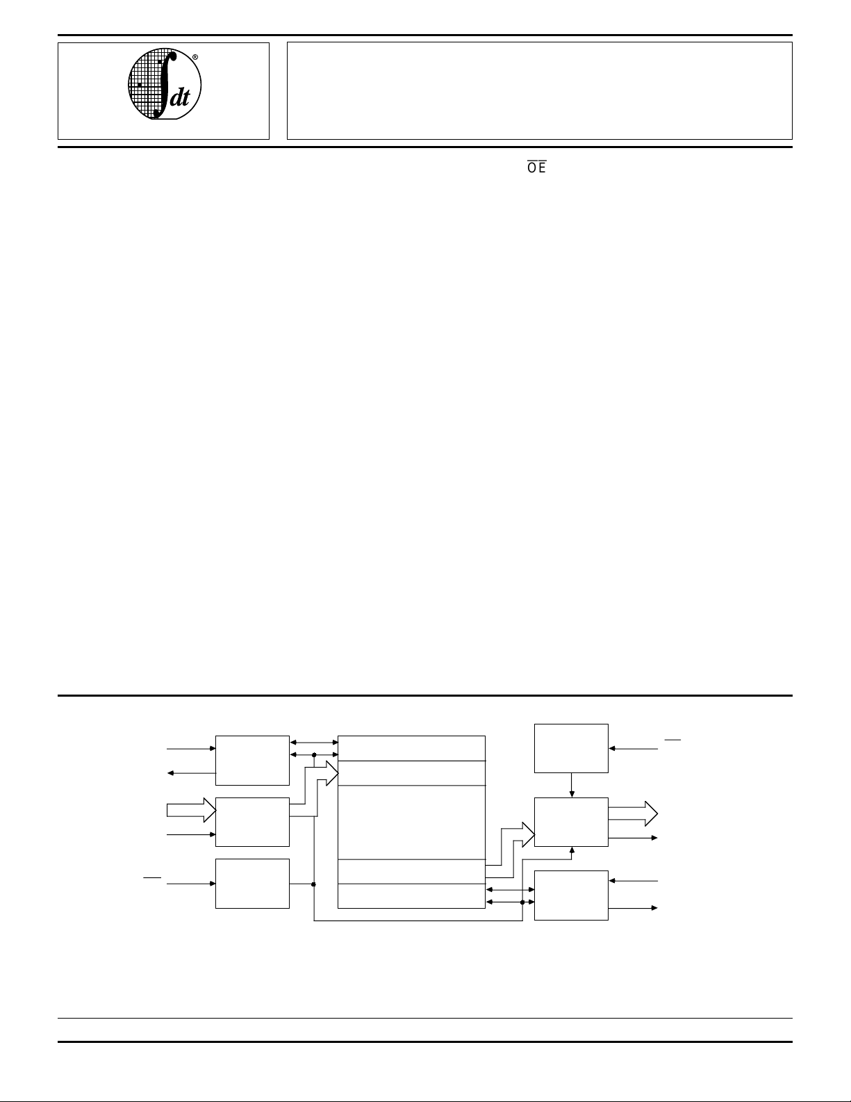
FUNCTIONAL BLOCK DIAGRAM
SI
IR
D
0-3
D
4
(IDT72402
and IDT72404)
MR
The IDT logo is a registered trademark of Integrated Device Technology, Inc.
FAST is a trademark of National Semiconductor, Inc.
INPUT
CONTROL
LOGIC
DATA
IN
MASTER
RESET
WRITE POINTER
WRITE MULTIPLEXER
MEMORY
ARRAY
READ MULTIPLEXER
READ POINTER
MILITARY AND COMMERCIAL TEMPERATURE RANGES SEPTEMBER 1996
1996 Integrated Device Technology, Inc. DSC-2747/7
For latest information contact IDT's web site at www.idt.com or fax-on-demand at 408-492-8391.
5.01 1
OUTPUT
ENABLE
DATA
OUT
OUTPUT
CONTROL
LOGIC
OE (IDT72403 and
IDT72404)
Q
0-3
Q4
(IDT72402 and
IDT72404)
SO
OR
2747 drw 01
Page 2
IDT72401, IDT72402, IDT72403, IDT72404
CMOS PARALLEL FIFO 64 x 4-BIT AND 64 x 5-BIT MILITARY AND COMMERCIAL TEMPERATURE RANGES
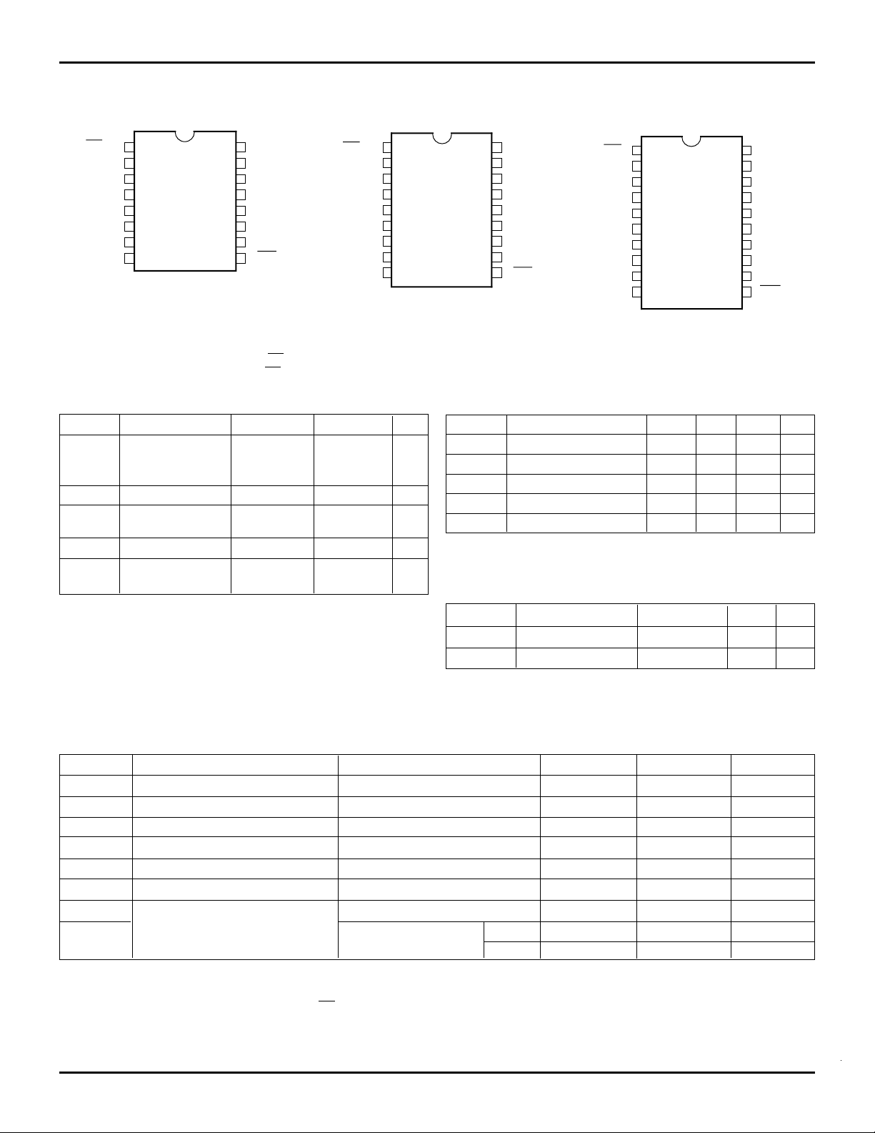
PIN CONFIGURATIONS
IDT72401/IDT72403
(1)
NC/OE
GND
NOTES:
1. Pin 1: NC - No Connection IDT72401,
2. Pin 1: NC - No Connection IDT72402,
1
2
IR
3
SI
0
D
D1
D2
D
3 3
P16-1,
4
5
S016-1
6
7
8
DIP/SOIC
TOP VIEW
D16-1
16
Vcc
15
SO
14
OR
13
Q
&
12
11
10
9
0
Q1
Q
2
Q
MR
2747 drw 02
OE - IDT72403
OE - IDT72404
ABSOLUTE MAXIMUM RATINGS
NC/OE
GND
(1)
IDT72402/IDT72404
(2)
1
2
IR
3
SI
4
0
D
5
D
1
6
D
2
7
D
3 3
8
D
4
9
DIP/SOIC
TOP VIEW
Symbol Rating Commercial Military Unit
V
TERM Terminal Voltage –0.5 to +7.0 –0.5 to +7.0 V
with Respect
to GND
T
A Operating Temp. 0 to +70 –55 to +125 ° C
BIAS Temperature –55 to +125 –65 to +135 °C
T
Under Bias
T
STG Storage Temp. –55 to +125 –65 to +150 ° C
OUT DC Output 50 50 mA
I
Current
NOTE: 2747 tbl 01
1. Stresses greater than those listed under ABSOLUTE MAXIMUM
RATINGS may cause permanent damage to the device. This is a stress
rating only and functional operation of the device at these or any other
conditions above those indicated in the operational sections of this
specification is not implied. Exposure to absolute maximum rating
conditions for extended periods may affect reliability.
(IDT72404 Only)
18
P18-1,
D18-1
&
S018-1
17
16
15
14
13
12
11
10
Vcc
SO
OR
Q
0
Q
1
Q
2
Q
Q
4
MR
2747 drw 03
OE
NC
GND
IR
SI
D0
D1
D2
D3
D4
1
2
3
4
5
6
7
8
9
10
CERPACK
TOP VIEW
20
19
18
17
16
15
14
13
12
11
RECOMMENDED OPERATING CONDITIONS
Symbol Parameter Min. Typ. Max. Unit
CC Mil. Supply Voltage 4.5 5.0 5.5 V
V
V
CC Com'l. Supply Voltage 4.5 5.0 5.5 V
GND Supply Voltage 0 0 0 V
IH Input High Voltage 2.0 — — V
V
(1)
IL
V
NOTE: 2747 tbl 02
1. 1.5V undershoots are allowed for 10ns once per cycle.
Input High Voltage — — 0.8 V
CAPACITANCE (TA = +25°C, f = 1.0MHz)
Symbol Parameter
IN Input Capacitance VIN = 0V 5 pF
C
OUT Output Capacitance VOUT = 0V 7 pF
C
NOTE: 2747 tbl 03
1. This parameter is sampled and not 100% tested.
(1)
Conditions Max. Unit
Vcc
NC
SO
OR
0
Q
Q1
Q2
Q3
4
Q
MR
2747 drw 04
DC ELECTRICAL CHARACTERISTICS
(Commercial: VCC = 5.0V ± 10%, TA = 0°C to +70°C; Military: VCC = 5.0V ± 10%, TA = –55°C to +125°C)
Symbol Parameter Test Conditions Min. Max. Unit
IL Low-Level Input Current VCC = Max., GND ≤ VI ≤ VCC –10 — µA
I
I
IH High-Level Input Current VCC = Max., GND ≤ VI ≤ VCC —10µA
OL Low-Level Output Voltage VCC = Min., IOL = 8mA — 0.4 V
V
OH High-Level Output Voltage VCC = Min., IOH = -4mA 2.4 — V
V
(1)
I
OS
HZ Off-State Output Current VCC = Max., VO = 2.4V — 20 µA
I
LZ (IDT72403 and IDT72404) VCC = Max., VO = 0.4V –20 — µA
I
(2,3)
CC
I
NOTES: 2747 tbl 04
1. Not more than one output should be shorted at a time and duration of the short-circuit should not exceed one second. Guaranteed but not tested.
CC measurements are made with outputs open. OE is HIGH for IDT72403/72404.
2. I
3 For frequencies greater than 10MHZ, I
Output Short-Circuit Current VCC = Max., VO = GND –20 –110 mA
Supply Current VCC = Max., f = 10MHz Com'l. — 35 mA
Military — 45 mA
CC = 35mA + (1.5mA x [f - 10MHz]) commercial, and ICC = 45mA + (1.5mA x [f - 10MHz]) military.
5.01 2
Page 3
IDT72401, IDT72402, IDT72403, IDT72404
CMOS PARALLEL FIFO 64 x 4-BIT AND 64 x 5-BIT MILITARY AND COMMERCIAL TEMPERATURE RANGES
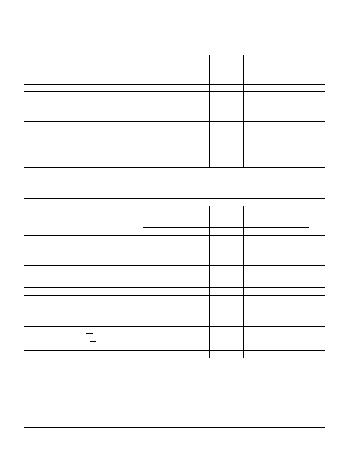
OPERATING CONDITIONS
(Commercial: VCC = 5.0V ± 10%, TA = 0°C to +70°C; Military: VCC = 5.0V ± 10%, TA = –55°C to +125°C)
Commercial Military and Commercial
IDT72401L45 IDT72401L35 IDT72401L25 IDT72401L15 IDT72401L10
IDT72402L45 IDT72402L35 IDT72402L25 IDT72402L15 IDT72402L10
IDT72403L45 IDT72403L35 IDT72403L25 IDT72403L15 IDT72403L10
IDT72404L45 IDT72404L35 IDT72404L25 IDT72404L15 IDT72404L10
Symbol Parameters FIgure Min. Max. Min. Max. Min. Max. Min. Max. Min. Max. Unit
(1)
t
SIH
SIL Shift in LOW TIme 2 11 — 17 — 24 — 25 — 30 — ns
t
t
IDS Input Data Set-up 2 0 — 0 — 0 — 0 — 0 — ns
t
IDH Input Data Hold Time 2 13 — 15 — 20 — 30 — 40 — ns
SOH
t
t
SOL Shift Out LOW Time 5 11 — 17 — 24 — 25 — 25 — ns
MRW Master Reset Pulse 8 20 — 25 — 25 — 25 — 30 — ns
t
t
MRS Master Reset Pulse to SI 8 10 — 10 — 10 — 25 — 35 — ns
t
SIR Data Set-up to IR 4 3 — 3 — 5 — 5 — 5 — ns
HIR Data Hold from IR 4 13 — 15 — 20 — 30 — 30 — ns
t
t
SOR
Shift in HIGH Time 2 9 — 9 — 11 — 11 — 11 — ns
(1)
Shift Out HIGH Time 5 9 — 9 — 11 — 11 — 11 — ns
(4)
Data Set-up to OR HIGH 7 0 — 0 — 0 — 0 — 0 — ns
2747 tbl 05
AC ELECTRICAL CHARACTERISTICS
(Commercial: VCC = 5.0V ± 10%, TA = 0°C to +70°C; Military: VCC = 5.0V ± 10%, TA = –55°C to +125°C)
Commercial Military and Commercial
IDT72401L45 IDT72401L35 IDT72401L25 IDT72401L15 IDT72401L10
IDT72402L45 IDT72402L35 IDT72402L25 IDT72402L15 IDT72402L10
IDT72403L45 IDT72403L35 IDT72403L25 IDT72403L15 IDT72403L10
IDT72404L45 IDT72404L35 IDT72404L25 IDT72404L15 IDT72404L10
Symbol Parameters FIgure Min. Max. Min. Max. Min. Max. Min. Max. Min. Max. Unit
t
IN Shift In Rate 2 — 45 — 35 — 25 — 15 — 10 MHz
(1)
t
IRL
t
IRH
OUT Shift Out Rate 5 — 45 — 35 — 25 — 15 — 10 MHz
t
t
ORL
ORH
t
t
ODH Output Data Hold (Previous Word) 5 5 — 5 — 5 — 5 — 5 — ns
ODS Output Data Shift (Next Word) 5 — 19 — 20 — 34 — 40 — 55 ns
t
t
PT Data Throughput or "Fall-Through" 4, 7 — 30 — 34 — 40 — 65 — 65 ns
t
MRORL Master Reset to OR LOW 8 — 25 — 28 — 35 — 35 — 40 ns
MRIRH Master Reset to IR HIGH 8 — 25 — 28 — 35 — 35 — 40 ns
t
MRQ Master Reset to Data Output LOW 8 — 20 — 20 — 25 — 35 — 40 ns
t
OOE
t
t
HZOE
IPH
t
OPH
t
NOTES:
1. Since the FIFO is a very high-speed device, care must be excercised in the design of the hardware and timing utilized within the design. Device grounding
and decoupling are crucial to correct operation as the FIFO will respond to very small glitches due to long reflective lines, high capacitances and/or poor
supply decoupling and grounding. A monolithic ceramic capacitor of 0.1µF directly between V
2. This parameter applies to FIFOs communicating with each other in a cascaded mode. IDT FIFOs are guaranteed to cascade with other IDT FIFOs of
like speed grades.
3. IDT72403 and IDT72404 only.
4. Guaranteed by design but not currently tested.
Shift In to Input Ready LOW 2 — 18 — 18 — 21 — 35 — 40 ns
(1)
Shift In to Input Ready HIGH 2 — 18 — 20 — 28 — 40 — 45 ns
(1)
Shift Out to Output Ready LOW 5 — 18 — 18 — 19 — 35 — 40 ns
(1)
Shift Out to Output Ready HIGH 5 — 19 — 20 — 34 — 40 — 55 ns
(3)
Output Valid from OE LOW 9 — 12 — 15 — 20 — 30 — 35 ns
(3,4)
Output High-Z from OE HIGH 9 — 12 — 12 — 15 — 25 — 30 ns
(2,4)
Input Ready Pulse HIGH 4 9 — 9 — 11 — 11 — 11 — ns
(2,4)
Ouput Ready Pulse HIGH 7 9 — 9 — 11 — 11 — 11 — ns
CC and GND with very short lead length is recommended.
2747 tbl 06
5.01 3
Page 4
IDT72401, IDT72402, IDT72403, IDT72404
CMOS PARALLEL FIFO 64 x 4-BIT AND 64 x 5-BIT MILITARY AND COMMERCIAL TEMPERATURE RANGES
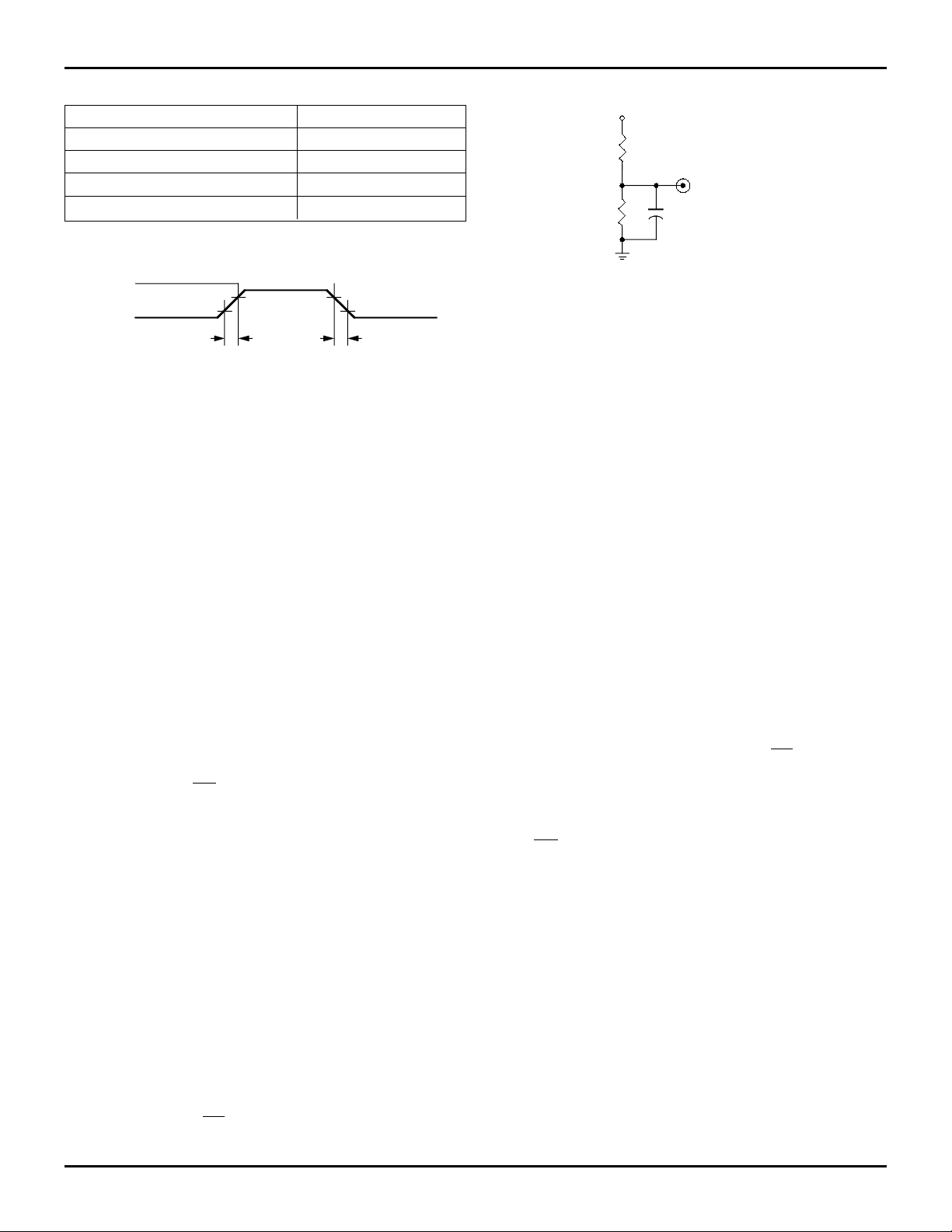
AC TEST CONDITIONS
Input Pulse Levels GND to 3.0V
Input Rise/Fall Times 3ns
Input Timing Reference Levels 1.5V
Output Reference Levels 1.5V
Output Load See Figure 1
2747 tbl 07
ALL INPUT PULSES:
3.0V
GND
90%
10%
<3ns <3ns
90%
10%
2747 drw 05
SIGNAL DESCRIPTIONS
INPUTS:
DATA INPUT (D0-3, 4)
Data input lines. The IDT72401 and IDT72403 have a 4-bit
data input. The IDT72402 and IDT72404 have a 5-bit data
input.
5V
560
Ω
OUTPUT
1.1K
Ω
Figure 1. AC Test Load
30pF*
or equivalent
*Including scope and jig
circuit
2747 drw 06
OUTPUTS:
DATA OUTPUT (Q0-3, 4)
Data Output lines. The IDT72401 and IDT72403 have a 4bit data output. The IDT72402 and IDT72404 have a 5-bit data
output.
FUNCTIONAL DESCRIPTION
CONTROLS:
SHIFT IN (SI)
Shift In controls the input of the data into the FIFO. When
SI is HIGH, data can be written to the FIFO via the D0-3, 4 lines.
SHIFT OUT (SO)
Shift Out controls the output of data of the FIFO. When SO
is HIGH, data can be read from the FIFO via the Data Output
(Q
0-3, 4) lines.
MASTER RESET (MR)
Master Reset clears the FIFO of any data stored within.
Upon power up, the FIFO should be cleared with a Master
Reset. Master Reset is active LOW.
INPUT READY (IR)
When Input Ready is HIGH, the FIFO is ready for new input
data to be written to it. When IR is LOW the FIFO is unavailable
for new input data. Input Ready is also used to cascade many
FlFOs together, as shown in Figures 10 and 11 in the Applications section.
OUTPUT READY (OR)
When Output Ready is HIGH, the output (Q0-3, 4) contains
valid data. When OR is LOW, the FIFO is unavailable for new
output data. Output Ready is also used to cascade many
FlFOs together, as shown in Figures 10 and 11.
These 64 x 4 and 64 x 5 FIFOs are designed using a dual
port RAM architecture as opposed to the traditional shift
register approach. This FIFO architecture has a write pointer,
a read pointer and control logic, which allow simultaneous
read and write operations. The write pointer is incremented by
the falling edge of the Shift In (Sl) control; the read pointer is
incremented by the falling edge of the Shift Out (SO). The
Input Ready (IR) signals when the FIFO has an available
memory location; Output Ready (OR) signals when there is
valid data on the output. Output Enable (
OE) provides the
capability of three-stating the FIFO outputs.
FIFO Reset
The FIFO must be reset upon power up using the Master
Reset (MR) signal. This causes the FlFO to enter an empty
state, signified by Output Ready (OR) being LOW and Input
Ready (IR) being HIGH. In this state, the data outputs (Q0-3,
4) will be LOW.
Data Input
Data is shifted in on the LOW-to-HlGH transition of Shift In
(Sl). This loads input data into the first word location of the
FIFO and causes Input Ready to go LOW. On the HlGH-toLOW transition of Shift In, the write pointer is moved to the next
word position and Input Ready (IR) goes HIGH, indicating the
readiness to accept new data. If the FIFO is full, Input Ready
will remain LOW until a word of data is shifted out.
OUTPUT ENABLE (
OE) (IDT72403 AND IDT72404 ONLY)
Output enable is used to read FIFO data onto a bus. Output
Enable is active LOW.
5.01 4
Page 5
IDT72401, IDT72402, IDT72403, IDT72404
CMOS PARALLEL FIFO 64 x 4-BIT AND 64 x 5-BIT MILITARY AND COMMERCIAL TEMPERATURE RANGES
Data Output
Data is shifted out on the HlGH-to-LOW transition of Shift
Out (SO). This causes the internal read pointer to be
advanced to the next word location. If data is present, valid
data will appear on the outputs and Output Ready (OR) will
go HIGH. If data is not present, Output Ready will stay
LOW indicating the FIFO is empty. The last valid word read
from the FIFO will remain at the FlFOs output when it is empty.
When the FIFO is not empty, Output Ready (OR) goes LOW
on the LOW-to-HIGH transition of Shift Out. Previous data
remains on the output until the HIGH-to-LOW transition of
Shift Out (SO).
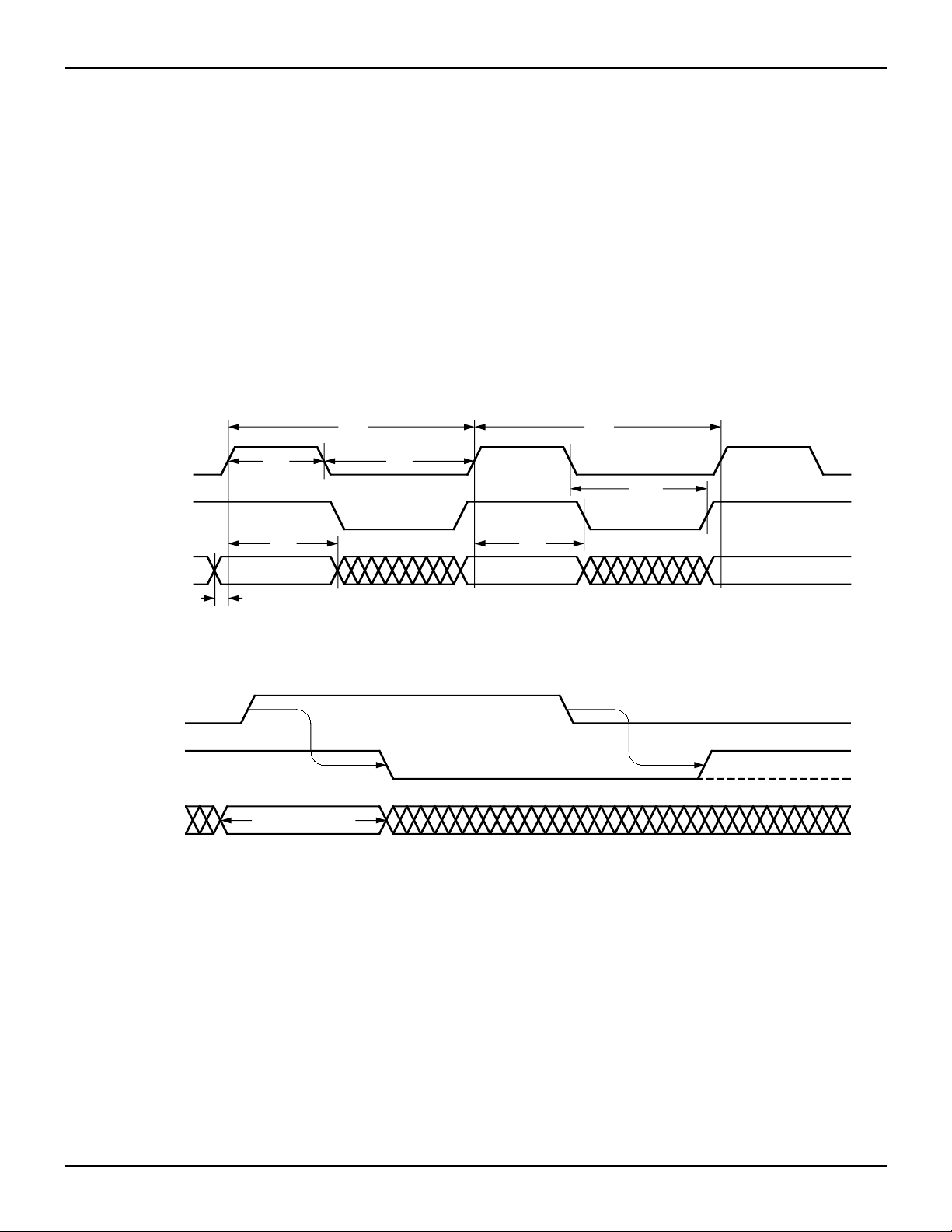
TIMING DIAGRAMS
1/f
IN
t
SHIFT IN
INPUT READY
SIH
t
IDH
t
SIL
Fall-Through Mode
The FIFO operates in a fall-through mode when data gets
shifted into an empty FIFO. After a fall-through delay the data
propagates to the output. When the data reaches the output,
the Output Ready (OR) goes HIGH. Fall-through mode also
occurs when the FIFO is completely full. When data is shifted
out of the full FIFO, a location is available for new data. After
a fall-through delay, the Input Ready goes HIGH. If Shift In is
HIGH, the new data can be written to the FIFO.
Since these FlFOs are based on an internal dual-port RAM
architecture with separate read and write pointers, the fallthrough time (tPT) is one cycle long. A word may be written
into the FIFO on a clock cycle and can be accessed on the next
clock cycle.
1/f
IN
t
IRH
t
IRL
INPUT DATA
t
IDS
Figure 2. Input Timing
SHIFT IN
(7)
INPUT READY
INPUT DATA
NOTES:
1. Input Ready HIGH indicates space is available and a Shift In pulse may be applied.
2. Input Data is loaded into the first word.
3. Input Ready goes LOW indicating the first word is full.
4. The write pointer is incremented.
5. The FIFO is ready for the next word.
6. If the FIFO is full then the Input Ready remains LOW.
7. Shift In pulses applied while Input Ready is LOW will be ignored (see Figure 4).
(2)
(1)
(3)
STABLE DATA
Figure 3. The Mechanism of Shifting Data Into the FIFO
2747 drw 07
(4)
(5)
(6)
2747 drw 08
5.01 5
Page 6
IDT72401, IDT72402, IDT72403, IDT72404
CMOS PARALLEL FIFO 64 x 4-BIT AND 64 x 5-BIT MILITARY AND COMMERCIAL TEMPERATURE RANGES
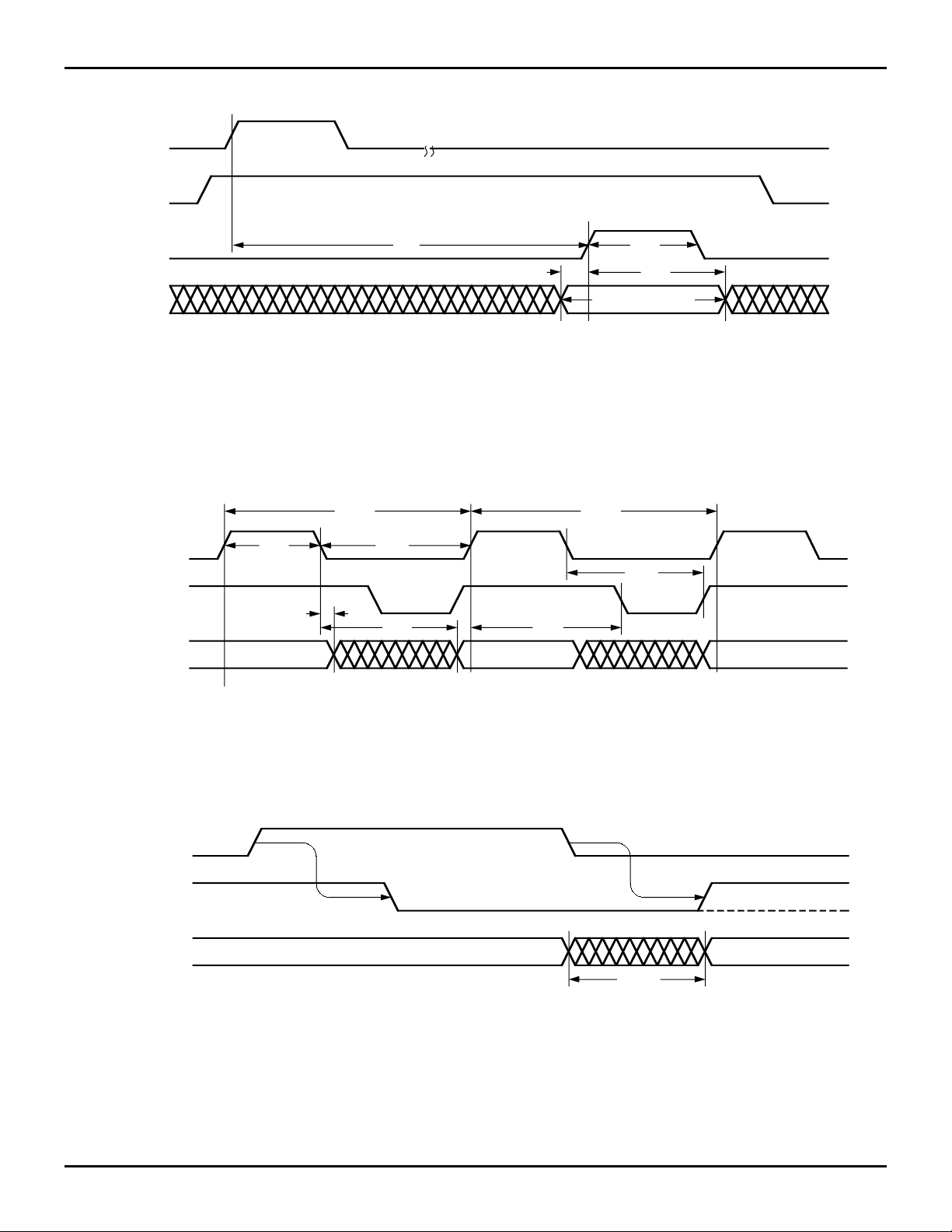
TIMING DIAGRAMS (Continued)
(2)
SHIFT OUT
(3)
SHIFT IN
(5)
INPUT READY
(1)
tPT
INPUT DATA
NOTES:
1. FIFO is initially full.
2. Shift Out pulse is applied.
3. Shift In is held HIGH.
4. As soon as Input Ready becomes HIGH the Input Data is loaded into the FIFO.
5. The write pointer is incremented. Shift In should not go LOW until (tPT + tIPH).
Figure 4. Data is Shifted In Whenever Shift In and Input Ready are Both HIGH
1/fOUT
SHIFT OUT
OUTPUT READY
OUTPUT DATA
NOTES:
1. This data is loaded consecutively A, B, C.
2. Data is shifted out when Shift Out makes a HIGH to LOW transition.
tSOH
tODH
A-DATA B-DATA
(1)
tSOL
(4)
t
SIR
t
IPH
t
HIR
STABLE DATA
2747 drw 09
1/fOUT
(2)
tORH
tORLtODS
C-DATA
2747 drw 10
Figure 5. Output TIming
SHIFT OUT
OUTPUT READY
OUTPUT DATA
(7)
(1)
(2)
A-DATA
(3)
(4)
(5)
(6)
B-DATA
A or B
NOTES:
1. Output Ready HIGH indicates that data is available and a Shift Out pulse may be applied.
2. Shift Out goes HIGH causing the next step.
3. Output Ready goes LOW.
4. The read pointer is incremented.
5. Output Ready goes HIGH indicating that new data (B) is now available at the FIFO outputs.
6. If the FIFO has only one word loaded (A DATA) then Output Ready stays LOW and the A DATA remains unchanged at the outputs.
7. Shift Out pulses applied when Output Ready is LOW will be ignored.
Figure 6. The Mechanism of Shifting Data Out of the FIFO
5.01 6
2747 drw 11
Page 7
IDT72401, IDT72402, IDT72403, IDT72404
CMOS PARALLEL FIFO 64 x 4-BIT AND 64 x 5-BIT MILITARY AND COMMERCIAL TEMPERATURE RANGES
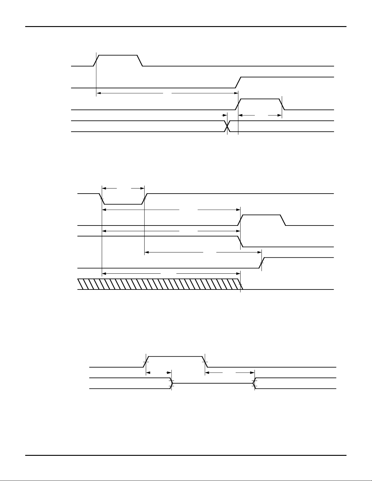
TIMING DIAGRAMS (Continued)
SHIFT IN
SHIFT OUT
tPT
OUTPUT READY
DATA OUTPUT
NOTE:
1. FIFO initially empty.
MASTER RESET
INPUT READY
OUTPUT READY
SHIFT IN
(1)
t
SOR
t
OPH
DATA VALID
2747 drw 12
Figure 7. t
-
PT and tOPH Specification
tMRW
tMRIRH
(1)
(1)
tMRORL
tMRS
tMRQ
DATA OUTPUT
NOTE:
1. Worst case, FIFO initially full..
OUTPUT ENABLE
DATA OUT
NOTE:
1. High-Z transitions are referenced to the steady-state V
instead of 30pF as shown in Figure 1.
Figure 9. Output Enable Timing, IDT72403 and IDT72404 Only
2747 drw 13
Figure 8. Master Reset Timing
HZOE
t
OH -500mV and VOL +500mV levels on the output. tHZOE is tested with 5pF load capacitance
OOE
t
2747 drw 14
5.01 7
Page 8
IDT72401, IDT72402, IDT72403, IDT72404
CMOS PARALLEL FIFO 64 x 4-BIT AND 64 x 5-BIT MILITARY AND COMMERCIAL TEMPERATURE RANGES
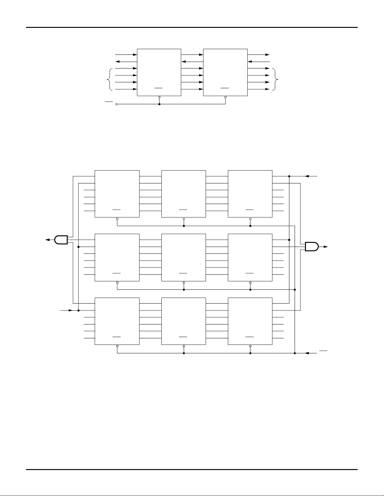
APPLICATIONS
SHIFT IN
INPUT READY
DATA IN
SI
IR
D0
D
D2
D
OR
SO
Q
0
1
Q1
Q2
3
MR
Q3
SI
IR
D0
D
D2
D
OR
SO
Q
0
1
Q1
Q2
3
MR
Q3
OUTPUT READY
SHIFT OUT
DATA OUT
2747 drw 15
MR
NOTE:
1. FIFOs can be easily cascaded to any desired path. The handshaking and associated timing between the FIFOs are handled by the inherent timing of
the devices.
Figure 10. 128 x 4 Depth Expansion
IR
SI
D
D
D
D
SO
OR
MR
Q
0
Q
1
Q
2
Q
3
0
1
2
3
IR
SI
D
D
D
D
SO
OR
0
1
2
3
MR
Q
0
Q
1
Q
2
Q
3
IR
SI
D
D
D
D
SO
OR
0
1
2
3
MR
Q
0
Q
1
Q
2
Q
3
SHIFT OUT
COMPOSITE
INPUT
READY
SHIFT IN
IR
SI
D
D
D
D
IR
SI
D
D
D
D
0
1
2
3
0
1
2
3
MR
MR
SO
OR
Q
Q
Q
Q
SO
OR
Q
Q
Q
Q
IR
SI
0
1
2
3
D
0
D
1
D
2
D
3
IR
SI
0
1
2
3
D
0
D
1
D
2
D
3
MR
MR
SO
OR
Q
Q
Q
Q
SO
OR
Q
Q
Q
Q
IR
SI
0
1
2
3
D
0
D
1
D
2
D
3
IR
SI
0
1
2
3
D
0
D
1
D
2
D
3
MR
MR
SO
OR
Q
Q
Q
Q
SO
OR
Q
Q
Q
Q
0
1
2
3
0
1
2
3
COMPOSITE
OUTPUT
READY
MR
2747 drw 16
NOTES:
1. When the memory is empty, the last word will remain on the outputs until the Master Reset is strobed or a new data word falls through to the output.
However, OR will remain LOW, indicating data at the output is not valid.
2. When the output data changes as a result of a pulse on SO, the OR signal always goes LOW before there is any change in output data and stays
LOW until the new data has appeared on the outputs. Anytime OR is HIGH, there is valid stable data on the outputs.
3. If SO is held HIGH while the memory is empty and a word is written into the input, that word will appear at the output after a fall-through time. OR will
go HIGH for one internal cycle (at least t
into the FIFO, they will line up behind the first word and will not appear on the outputs until SO has been brought LOW.
4. When the Master Reset is brought Low, the outputs are cleared to LOW, IR goes HIGH and OR goes LOW. If SI is HIGH when the Master Reset
goes HIGH, the data on the inputs will be written into the memory and IR will return to the LOW state until SI is brought LOW. If SI is LOW when the
Master Reset is ended, IR will go HIGH, but the data in the inputs will not enter the memory until SI goes HIGH.
5. FIFOs are expandable on depth and width. However, in forming wider words, two external gates are required to generate composite Input and
Output Ready flags. This is due to the variation of delays of the FIFOs.
ORL) and then go back LOW again. The stored word will remain on the outputs. If more words are written
Figure 11. 192 x 12 Depth and Width Expansion
5.01 8
Page 9
IDT72401, IDT72402, IDT72403, IDT72404
CMOS PARALLEL FIFO 64 x 4-BIT AND 64 x 5-BIT MILITARY AND COMMERCIAL TEMPERATURE RANGES
ORDERING INFORMATION
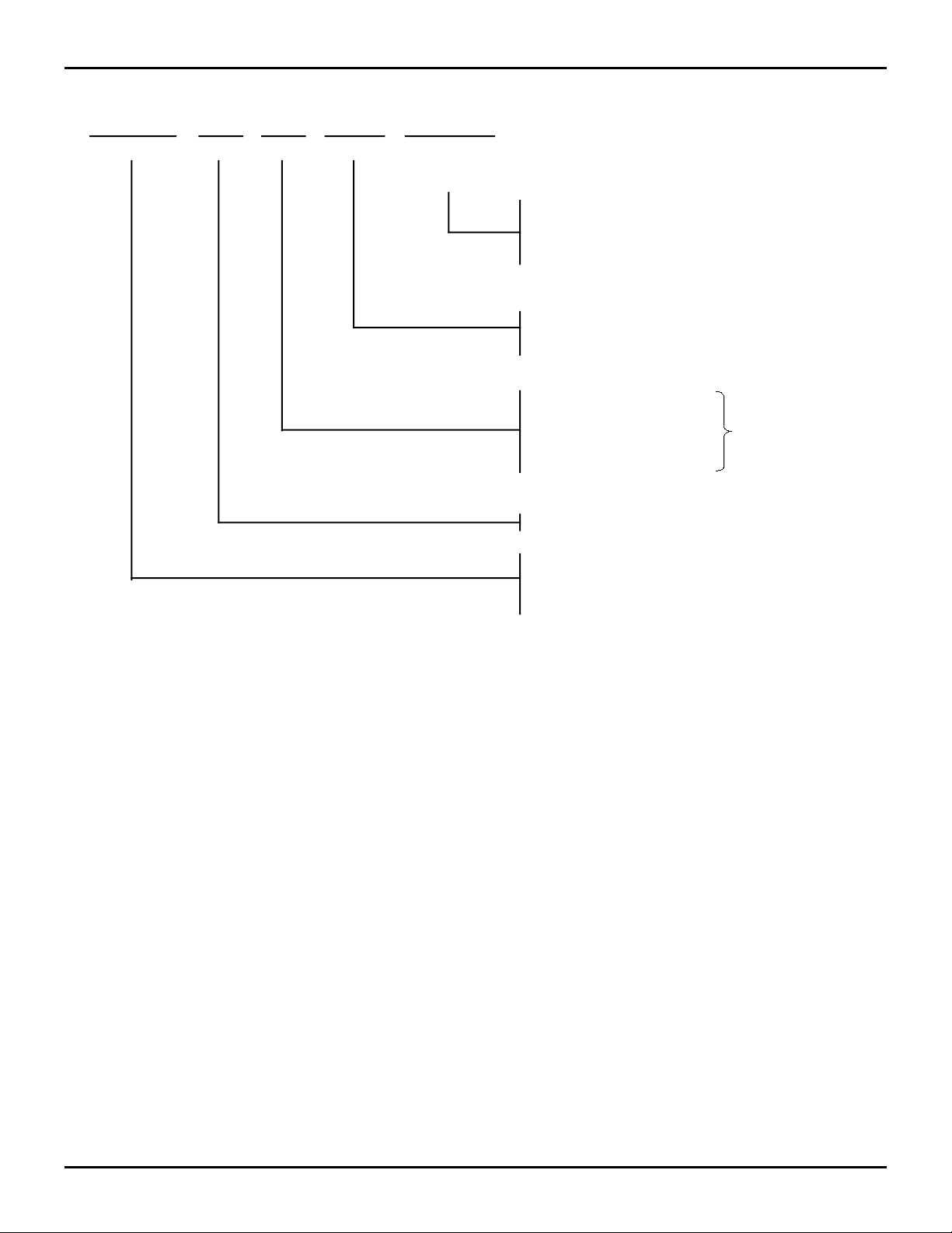
IDT XXXXX
X
X
X
X
Device Type
Power
Speed
Package
Process/
Temperature
Range
Blank
B
P
D
SO
Commercial (0°C to+70°C)
Military (–55°C to+125°C)
Compliant to MIL-STD-883, Class B
Plastic DIP (300 mils wide)
Ceramic DIP (300 mils wide)
Small Outline IC
45
35
25
15
10
L
72401
72402
72403
72404
Com’l. Only
Com'l. and Mil
Com’l. and Mil
Com'l. and Mil
Com'l. and Mil
Low Power
64 x 4 FIFO
64 x 5 FIFO
64 x 4 FIFO
64 x 5 FIFO
Shift Frequency (fs)
Speed in MHz
2747 drw 17
5.01 9
Page 10

WWW.ALLDATASHEET.COM
Copyright © Each Manufacturing Company.
All Datasheets cannot be modified without permission.
This datasheet has been download from :
www.AllDataSheet.com
100% Free DataSheet Search Site.
Free Download.
No Register.
Fast Search System.
www.AllDataSheet.com
 Loading...