

查询IDT72V72100供应商
3.3 VOLT HIGH-DENSITY SUPERSYNC II™ 72-BIT FIFO
512 x 72, 1,024 x 72
2,048 x 72, 4,096 x 72
8,192 x 72, 16,384 x 72
32,768 x 72, 65,536 x 72
FEATURES:
••
Choose among the following memory organizations:
•
••
IDT72V7230
IDT72V7240
IDT72V7250
IDT72V7260
IDT72V7270
IDT72V7280
IDT72V7290
IDT72V72100
••
• 100 MHz operation (10 ns read/write cycle time)
••
••
User selectable input and output port bus-sizing
•
••
- x72 in to x72 out
- x72 in to x36 out
- x72 in to x18 out
- x36 in to x72 out
- x18 in to x72 out
••
•
Big-Endian/Little-Endian user selectable word representation
••
••
• Fixed, low first word latency
••
••
• Zero latency retransmit
••
••
• Auto power down minimizes standby power consumption
••
512 x 72
1,024 x 72
2,048 x 72
4,096 x 72
8,192 x 72
16,384 x 72
32,768 x 72
65,536 x 72
IDT72V7230, IDT72V7240
IDT72V7250, IDT72V7260
IDT72V7270, IDT72V7280
IDT72V7290, IDT72V72100
••
•
Master Reset clears entire FIFO
••
••
•
Partial Reset clears data, but retains programmable settings
••
••
•
Empty, Full and Half-Full flags signal FIFO status
••
••
• Programmable Almost-Empty and Almost-Full flags, each flag can
••
default to one of eight preselected offsets
••
• Selectable synchronous/asynchronous timing modes for Almost-
••
Empty and Almost-Full flags
••
• Program programmable flags by either serial or parallel means
••
••
• Select IDT Standard timing (using EF and FF flags) or First Word
••
Fall Through timing (using OR and IR flags)
••
Output enable puts data outputs into high impedance state
•
••
••
• Easily expandable in depth and width
••
••
• Independent Read and Write Clocks (permit reading and writing
••
simultaneously)
••
• Asynchronous operation of Output Enable, OE
••
••
•
Read Chip Select ( RCS ) on Read Side
••
••
• Available in a 256-pin Fine Pitch Ball Grid Array package (PBGA)
••
••
• Features JTAG (Boundary Scan)
••
••
• High-performance submicron CMOS technology
••
••
• Industrial temperature range (–40
••
°°
°C to +85
°°
°°
°C) is available
°°
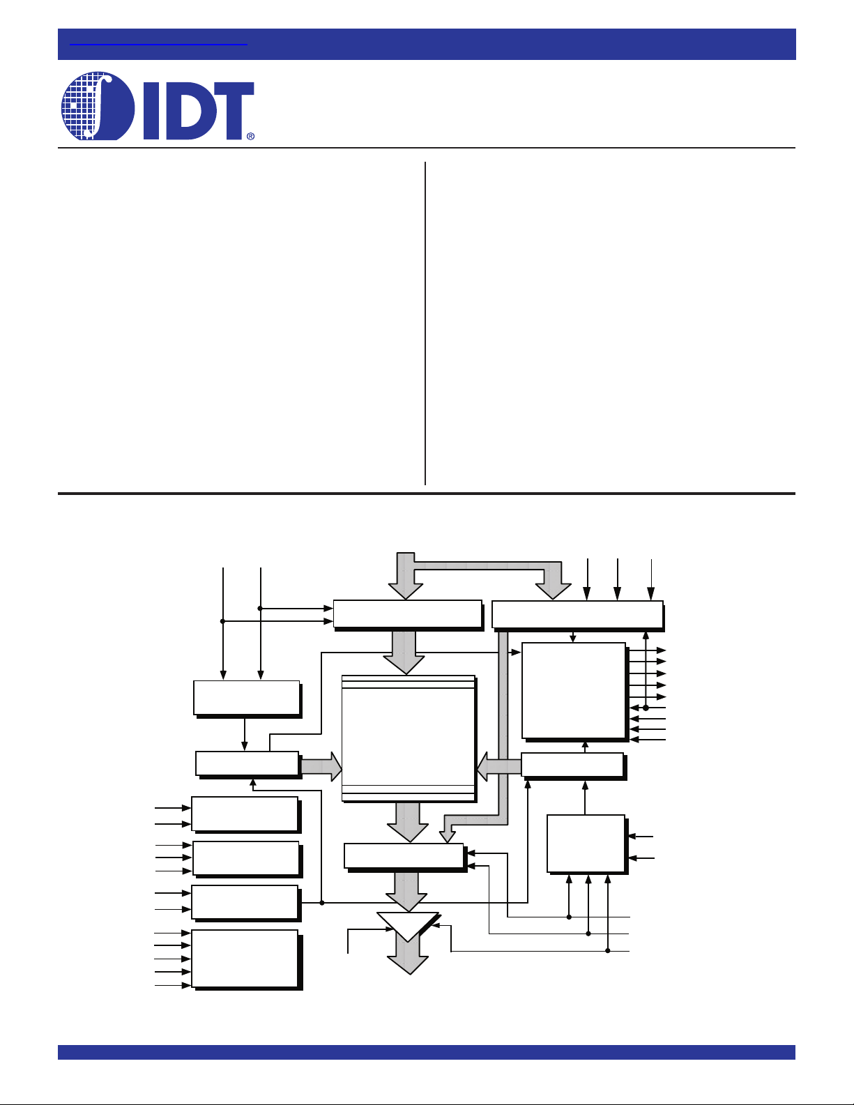
FUNCTIONAL BLOCK DIAGRAM
WEN
WCLK
WRITE CONTROL
LOGIC
WRITE POINTER
BE
IP
BM
IW
OW
MRS
PRS
TCK
TRST
TMS
TDO
TDI
CONTROL
LOGIC
BUS
CONFIGURATION
RESET
LOGIC
JTAG
CONTROL
(BOUNDARY SCAN)
OE
0
-D
n
(x72, x36 or x18)
D
INPUT REGISTER
RAM ARRAY
512 x 72
1,024 x 72
2,048 x 72
4,096 x 72
8,192 x 72
16,384 x 72
32,768 x 72
65,536 x 72
OUTPUT REGISTER
Q0 -Qn (x72, x36 or x18)
LD
SEN
OFFSET REGISTER
FLAG
LOGIC
READ POINTER
READ
CONTROL
LOGIC
SCLK
RCLK
REN
RCS
FF/IR
PAF
EF/OR
PAE
HF
FWFT/SI
PFM
FSEL0
FSEL1
RT
RM
4680 drw01
IDT and the IDT logo are registered trademarks of Integrated Device Technology, Inc. SuperSync II FIFO is a trademark of Integrated Device Technology, Inc.
COMMERCIAL TEMPERATURE RANGE
1
2003 Integrated Device Technology, Inc. All rights reserved. Product specifications subject to change without notice.
DECEMBER 2003
DSC-4680/9
IDT72V7230/7240/7250/7260/7270/7280/7290/72100 3.3V HIGH DENSITY SUPERSYNC IITM FIFO
512 x 72, 1K x 72, 2K x 72, 4K x 72, 8K x 36, 16K x 72, 32K x 72, 64K x 72
COMMERCIAL TEMPERATURE RANGE
DESCRIPTION:
The IDT72V7230/72V7240/72V7250/72V7260/72V7270/72V7280/
72V7290/72V72100 are exceptionally deep, high speed, CMOS First-In-FirstOut (FIFO) memories with clocked read and write controls and a flexible BusMatching x72/x36/x18 data flow.
These FIFOs offer several key user benefits:
• Flexible x72/x36/x18 Bus-Matching on both read and write ports
• The period required by the retransmit operation is fixed and short.
• The first word data latency period, from the time the first word is written to an
empty FIFO to the time it can be read, is fixed and short.
• High density offerings up to 4 Mbit
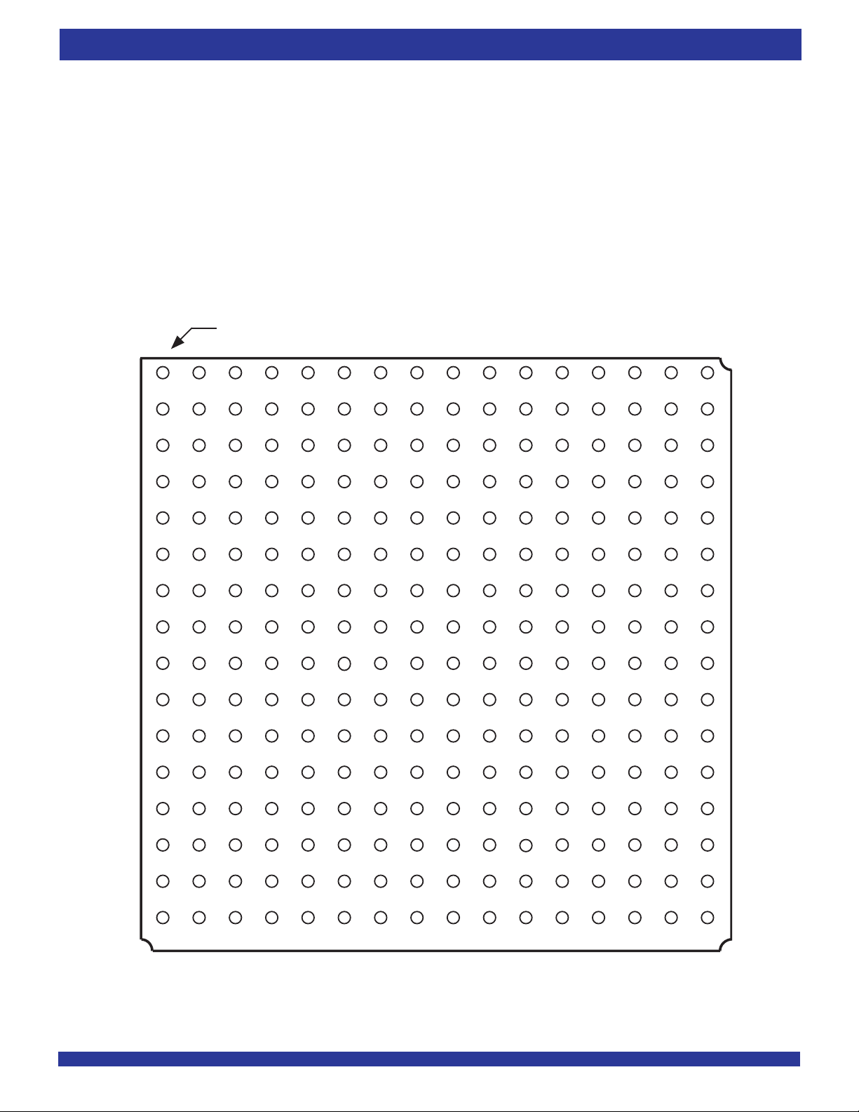
PIN CONFIGURATION
A1 BALL PAD CORNER
A
Q33
Q35
Q47
Q50
Q53
Q65
B
Q32
Q34
Q46
Q49
Q52
Q64
C
Q30
Q45
Q31
Q48
Q51
Q63
D
Q29
Q28
Q27
VCC
GND
VCC
E
GND
Q17
Q16
Q15
VCC
VCC
F
VCC
Q14
Q13
Q12
GND
VCC
G
Q11
Q10
Q9
VCC
GND
VCC
H
VCC
GND
Q62
Q61
Q60
VCC
J
VCC
GND
Q59
Q58
Q57
VCC
K
VCC
GND
Q56
Q55
Q54
VCC
L
Q44
Q43
Q42
VCC
GND
VCC
M
Q41
Q40
Q39
VCC
GND
VCC
N
RT
RM
Q38
Q37
Q36
PFM
P
Q26
Q25
Q18
Q6
Q3
Q0
R
Q24
Q21
Q19
Q7
Q4
Q1
T
Q23
Q22
Q20
Q8
Q5
Q2
Q68
Q67
Q66
GND
GND
GND
GND
GND
GND
GND
GND
GND
BM
RCS
OE
REN
Q71
Q70
Q69
TCK
VCC
VCC
VCC
VCC
VCC
VCC
GND
PAE
RCLK
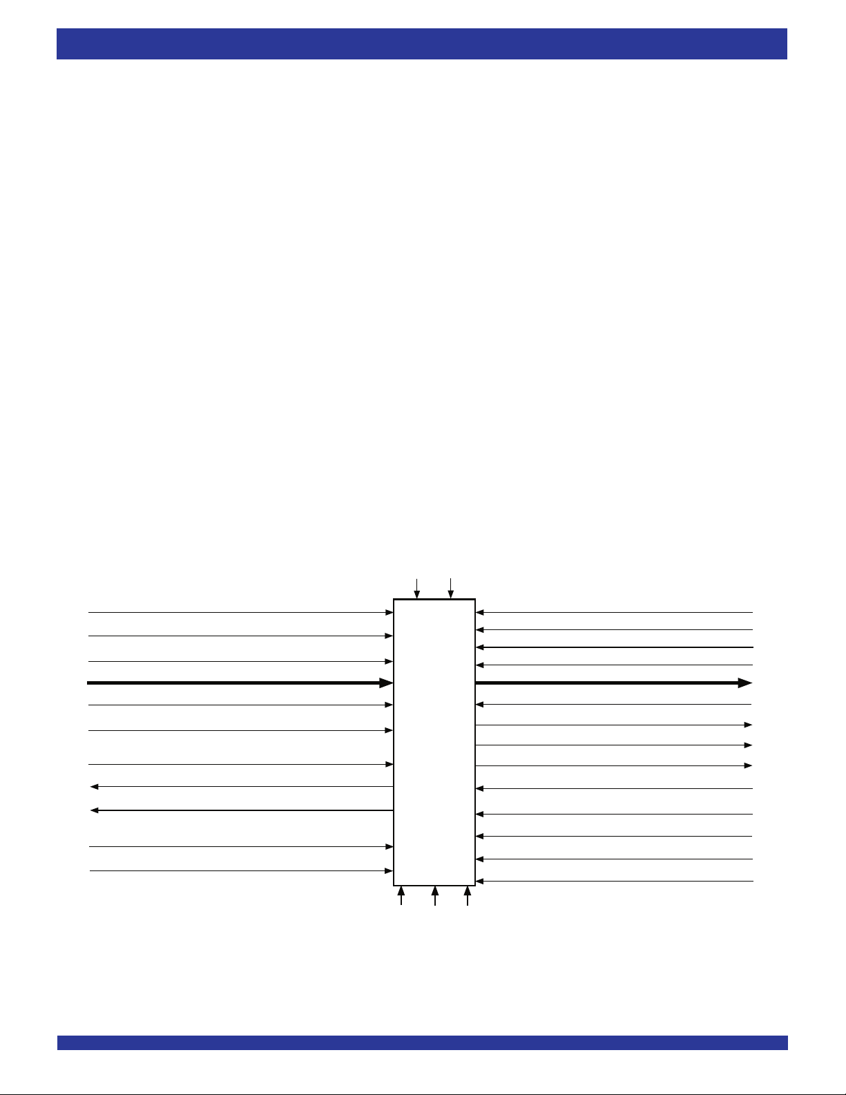
Bus-Matching Sync FIFOs are particularly appropriate for network, video,
telecommunications, data communications and other applications that need to
buffer large amounts of data and match busses of unequal sizes.
Each FIFO has a data input port (D
n) and a data output port (Qn), both of
which can assume either a 72-bit, 36-bit or a 18-bit width as determined by the
state of external control pins Input Width (IW), Output Width (OW), and BusMatching (BM) pin during the Master Reset cycle.
The input port is controlled by a Write Clock (WCLK) input and a Write Enable
(WEN) input. Data is written into the FIFO on every rising edge of WCLK when
WEN is asserted. The output port is controlled by a Read Clock (RCLK) input
IP
EF
D71
D70
D69
TDI
GND
GND
GND
GND
GND
GND
GND
FS1
BE
MRS
PAF
FF
D68
D67
D66
TRST
VCC
VCC
VCC
VCC
VCC
VCC
VCC
FS0
HF
PRS
WEN
WCLK
D65
D64
D63
TDO
GND
GND
GND
GND
GND
GND
GND
OW
FWFT/
SI
D0
D1
D2
D50
D53
D49
D52
D48
D51
TMS
GND
VCC
GND
VCC
GND
GND
VCC
VCC
GND
VCC
GND
VCC
GND
GNDVCC
IW
GND SCLK
SEN
LD
D3
D6
D4
D7
D5
D8
D47
D46
D45
D27
D15
D12
D9
D60
D57
D54
D42
D39
D36
D18
D19
D20
D35
D34
D30
D28
D16
D13
D10
D61
D58
D55
D43
D40
D37
D25
D21
D22
D33
D32
D31
D29
D17
D14
D11
D62
D59
D56
D44
D41
D38
D26
D24
D23
12 3456 78910111213141516
4680 drw02
PBGA (BB256-1, order code: BB)
TOP VIEW
2
IDT72V7230/7240/7250/7260/7270/7280/7290/72100 3.3V HIGH DENSITY SUPERSYNC IITM FIFO
512 x 72, 1K x 72, 2K x 72, 4K x 72, 8K x 36, 16K x 72, 32K x 72, 64K x 72
COMMERCIAL TEMPERATURE RANGE
DESCRIPTION (CONTINUED)
and Read Enable (REN) input. Data is read from the FIFO on every rising edge
of RCLK when REN is asserted. An Output Enable (OE) input is provided for
three-state control of the outputs.
A Read Chip Select (RCS) input is also provided for synchronous enable
and disable of the read port control input, REN. The RCS input is synchronized
to the read clock, and also provides three-state control of the Q
RCS is disable, REN will be disabled internally and data outputs will be in
High-Impedance state.
The frequencies of both the RCLK and the WCLK signals may vary from 0
to fMAX with complete independence. There are no restrictions on the frequency
of the one clock input with respect to the other.
There are two possible timing modes of operation with these devices: IDT
Standard mode and First Word Fall Through (FWFT) mode.
In IDT Standard mode, the first word written to an empty FIFO will not appear
on the data output lines unless a specific read operation is performed. A read
operation, which consists of activating REN and enabling a rising RCLK edge,
will shift the word from internal memory to the data output lines.
In FWFT mode, the first word written to an empty FIFO is clocked directly
to the data output lines after three transitions of the RCLK signal. A REN does
not have to be asserted for accessing the first word. However, subsequent
words written to the FIFO do require a LOW on REN for access. The state of
the FWFT/SI input during Master Reset determines the timing mode in use.
n outputs. When
For applications requiring more data storage capacity than a single FIFO
can provide, the FWFT timing mode permits depth expansion by chaining FIFOs
in series (i.e. the data outputs of one FIFO are connected to the corresponding
data inputs of the next). No external logic is required.
These FIFOs have five flag pins, EF/OR (Empty Flag or Output Ready),
FF/IR (Full Flag or Input Ready), HF (Half-full Flag), PAE (Programmable
Almost-Empty flag) and PAF (Programmable Almost-Full flag). The EF and FF
functions are selected in IDT Standard mode. The IR and OR functions are
selected in FWFT mode. HF, PAE and PAF are always available for use,
irrespective of timing mode.
PAE and PAF can be programmed independently to switch at any point in
memory. Programmable offsets determine the flag switching threshold and can
be loaded by two methods: parallel or serial. Eight default offset settings are also
provided, so that PAE can be set to switch at a predefined number of locations
from the empty boundary and the PAF threshold can also be set at similar
predefined values from the full boundary. The default offset values are set during
Master Reset by the state of the FSEL0, FSEL1, and LD pins.
For serial programming, SEN together with LD on each rising edge of
SCLK, are used to load the offset registers via the Serial Input (SI). For parallel
programming, WEN together with LD on each rising edge of WCLK, are used
to load the offset registers via D
n. REN together with LD on each rising edge
of RCLK can be used to read the offsets in parallel from Qn regardless of whether
serial or parallel offset loading has been selected.
PARTIAL RESET (PRS)
WRITE CLOCK (WCLK)
WRITE ENABLE (WEN)
LOAD (LD)
(x72, x36, x18) DATA IN (D
0 - Dn)
SERIAL IN CLOCK(SCLK)
SERIAL ENABLE(SEN)
FIRST WORD FALL THROUGH/SERIAL INPUT
(FWFT/SI)
FULL FLAG/INPUT READY (FF/IR)
PROGRAMMABLE ALMOST-FULL (PAF)
INTERSPERSED/
NON-INTERSPERSED PARITY (IP)
BIG-ENDIAN/LITTLE-ENDIAN (BE)
INPUT WIDTH (IW)
MASTER RESET (MRS)
IDT
72V7230
72V7240
72V7250
72V7260
72V7270
72V7280
72V7290
72V72100
BUS-
MATCHING
(BM)
READ CLOCK (RCLK)
READ ENABLE (REN)
READ CHIP SELECT (RCS)
OUTPUT ENABLE (OE)
(x72, x36, x18) DATA OUT (Q0 - Qn)
RETRANSMIT (RT)
EMPTY FLAG/OUTPUT READY (EF/OR)
PROGRAMMABLE ALMOST-EMPTY (PAE)
HALF-FULL FLAG (HF)
JTAG CLOCK (TCLK)
JTAG RESET (TRST)
JTAG MODE (TMS)
(TDO)
(TDI)
OUTPUT WIDTH (OW)
4680 drw03
Figure 1. Single Device Configuration Signal Flow Diagram
3

IDT72V7230/7240/7250/7260/7270/7280/7290/72100 3.3V HIGH DENSITY SUPERSYNC IITM FIFO
512 x 72, 1K x 72, 2K x 72, 4K x 72, 8K x 36, 16K x 72, 32K x 72, 64K x 72
COMMERCIAL TEMPERATURE RANGE
During Master Reset (MRS) the following events occur: the read and write
pointers are set to the first location of the FIFO. The FWFT pin selects IDT
Standard mode or FWFT mode.
The Partial Reset (PRS) also sets the read and write pointers to the first
location of the memory. However, the timing mode, programmable flag
programming method, and default or programmed offset settings existing before
Partial Reset remain unchanged. The flags are updated according to the timing
mode and offsets in effect. PRS is useful for resetting a device in mid-operation,
when reprogramming programmable flags would be undesirable.
It is also possible to select the timing mode of the PAE (Programmable AlmostEmpty flag) and PAF (Programmable Almost-Full flag) outputs. The timing
modes can be set to be either asynchronous or synchronous for the PAE and
PAF flags.
If asynchronous PAE/PAF configuration is selected, the PAE is asserted
LOW on the LOW-to-HIGH transition of RCLK. PAE is reset to HIGH on the LOWto-HIGH transition of WCLK. Similarly, the PAF is asserted LOW on the LOWto-HIGH transition of WCLK and PAF is reset to HIGH on the LOW-to-HIGH
transition of RCLK.
If synchronous PAE/PAF configuration is selected , the PAE is asserted and
updated on the rising edge of RCLK only and not WCLK. Similarly, PAF is
asserted and updated on the rising edge of WCLK only and not RCLK. The
mode desired is configured during master reset by the state of the Programmable
Flag Mode (PFM) pin.
The Retransmit function allows data to be reread from the FIFO more than
once. A LOW on the RT input during a rising RCLK edge initiates a retransmit
operation by setting the read pointer to the first location of the memory array.
A zero-latency retransmit timing mode can be selected using the Retransmit
timing Mode pin (RM). During Master Reset, a LOW on RM will select zero
latency retransmit. A HIGH on RM during Master Reset will select normal
latency.
If zero latency retransmit operation is selected, the first data word to be
retransmitted will be placed on the output register with respect to the same RCLK
edge that initiated the retransmit based on RT being LOW.
Refer to Figure 16 and 17 for Retransmit Timing with normal latency. Refer
to Figure 18 and 19 for Zero Latency Retransmit Timing.
The device can be configured with different input and output bus widths as
shown in Table 1.
A Big-Endian/Little-Endian data word format is provided. This function is
useful when the FIFO is used in Bus-Matching mode, to determine order of the
words. As an example, if Big-Endian mode is selected, then the most significant
word of the long word written into the FIFO will be read out of the FIFO first,
followed by the least significant word. If Little-Endian format is selected, then the
least significant word of the long word written into the FIFO will be read out first,
followed by the most significant word. The mode desired is configured during
master reset by the state of the Big-Endian (BE) pin.
The Interspersed/Non-Interspersed Parity (IP) bit function allows the user
to select the parity bit in the word loaded into the parallel port (D0-Dn) when
programming the flag offsets. If Interspersed Parity mode is selected, then the
FIFO will assume that the parity bit is located in bit position D8 during the parallel
programming of the flag offsets. If Non-Interspersed Parity mode is selected,
then D8 is assumed to be a valid bit and D16 and D17 are ignored. IP mode
is selected during Master Reset by the state of the IP input pin.
If, at any time, the FIFO is not actively performing an operation, the chip will
automatically power down. Once in the power down state, the standby supply
current consumption is minimized. Initiating any operation (by activating control
inputs) will immediately take the device out of the power down state.
Both an Asynchronous Output Enable pin (OE) and Synchronous Read
Chip Select pin (RCS) are provided on the FIFO. The Synchronous Read
Chip Select is synchronized to the RCLK. Both the output enable and read chip
select control the output buffer of the FIFO, causing the buffer to be either HIGH
impedance or LOW impedance.
JTAG test pins are also provided, the FIFO has fully functional Boundary
Scan feature, compliant with IEEE 1149.1 Standard Test Access Port and
Boundary Scan Architecture.
The IDT72V7230/72V7240/72V7250/72V7260/72V7270/72V7280/
72V7290/72V72100 are fabricated using IDT’s high speed submicron CMOS
technology.
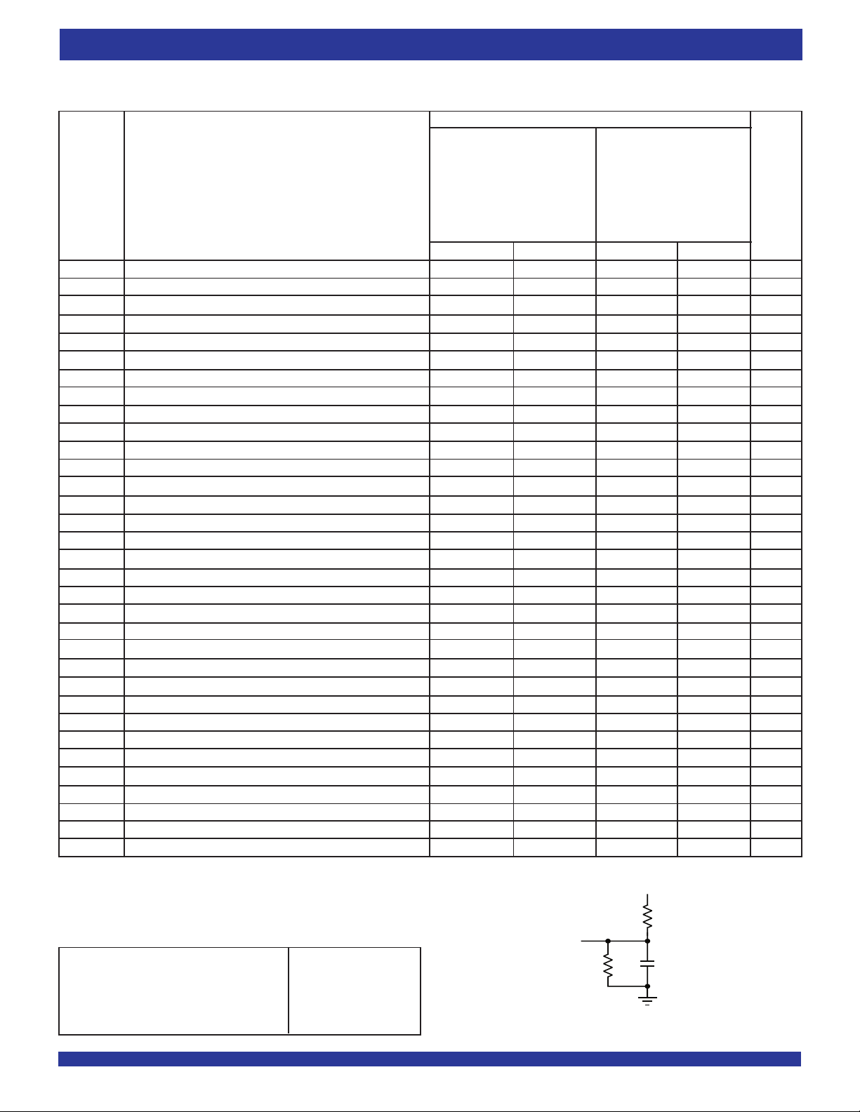
TABLE 1 — BUS-MATCHING CONFIGURATION MODES
BM IW OW Write Port Width Read Port Width
L X X x72 x72
H H L x36 x72
H H H x18 x72
H L L x72 x36
H L H x72 x18
4

IDT72V7230/7240/7250/7260/7270/7280/7290/72100 3.3V HIGH DENSITY SUPERSYNC IITM FIFO
512 x 72, 1K x 72, 2K x 72, 4K x 72, 8K x 36, 16K x 72, 32K x 72, 64K x 72
COMMERCIAL TEMPERATURE RANGE
PIN DESCRIPTION
Symbol Name I/O Description
D
0–D71 Data Inputs I Data inputs for a 72-, 36- or 18-bit bus. When in 36- or 18-bit mode, the unused input pins should be tied
LOW.
MRS Master Reset I MRS initializes the read and write pointers to zero and sets the output register to all zeroes. During Master Reset,
the FIFO is configured for either FWFT or IDT Standard mode, Bus-Matching configurations, one of eight
programmable flag default settings, serial or parallel programming of the offset settings, Big-Endian/Little-Endian
format, zero latency timing mode, interspersed parity, and synchronous versus asynchronous programmable
flag timing modes.
PRS Partial Reset I PRS initializes the read and write pointers to zero and sets the output register to all zeroes. During Partial Reset,
the existing mode (IDT or FWFT), programming method (serial or parallel), and programmable flag settings
are all retained.
RT Retransmit I RT asserted on the rising edge of RCLK initializes the READ pointer to zero, sets the EF flag to LOW (OR to
HIGH in FWFT mode) and does not disturb the write pointer, programming method, existing timing mode or
programmable flag settings. RT is useful to reread data from the first physical location of the FIFO.
FWFT/SI First Word Fall I During Master Reset, selects First Word Fall Through or IDT Standard mode. After Master Reset, this pin functions
Through/Serial In as a serial input for loading offset registers.
O W Output Width I This pin, along with IW and BM, selects the bus width of the read port. See Table 1 for bus size configuration.
I W Input Width I This pin, along with OW and BM, selects the bus width of the write port. See Table 1 for bus size configuration.
BM Bus-Matching I BM works with IW and OW to select the bus sizes for both write and read ports. See Table 1 for bus size
configuration.
BE Big-Endian/ I During Master Reset, a LOW on BE will select Big-Endian operation. A HIGH on BE during Master Reset
Little-Endian will select Little-Endian format.
RM Retransmit Timing I During Master Reset, a LOW on RM will select zero latency Retransmit timing Mode. A HIGH on RM will select
Mode normal latency mode.
PFM Programmable I During Master Reset, a LOW on PFM will select Asynchronous Programmable flag timing mode. A HIGH on
Flag Mode PFM will select Synchronous Programmable flag timing mode.
IP Interspersed Parity I During Master Reset, a LOW on IP will select Non-Interspersed Parity mode. A HIGH will select Interspersed
Parity mode.
FSEL0 Flag Select Bit 0 I During Master Reset, this input along with FSEL1 and the LD pin, will select the default offset values for the
programmable flags PAE and PAF. There are up to eight possible settings available.
FSEL1 Flag Select Bit 1 I During Master Reset, this input along with FSEL0 and the LD pin will select the default offset values for the
programmable flags PAE and PAF. There are up to eight possible settings available.
WCLK Write Clock I When enabled by WEN, the rising edge of WCLK writes data into the FIFO and offsets into the programmable
registers for parallel programming.
WEN Write Enable I WEN enables WCLK for writing data into the FIFO memory and offset registers.
RCLK Read Clock I When enabled by REN, the rising edge of RCLK reads data from the FIFO memory and offsets from the
programmable registers. (RCS must be active).
REN Read Enable I REN enables RCLK for reading data from the FIFO memory and offset registers. (RCS must be active).
OE Output Enable I OE provides asynchronous control of the output impedance of Q
input is the only input that provide High-Impedance control of the data outputs.
RCS Read Chip Select I RCS provides synchronous control of the read port and output impedance of Q
a Master or Partial Reset the RCS input is don’t care, if OE is LOW the data outputs will be Low-Impedance
regardless of RCS.
SCLK Serial Input Clock I when enabled by SEN, the rising edge of SCLK writes one bit of data (present on the SI input), into the
programmable register for serial programming.
SEN Serial Enable I SEN enables serial loading of programmable flag offsets.
LD Load I This is a dual purpose pin. During Master Reset, the state of the LD input along with FSEL0 and FSEL1,
determines one of eight default offset values for the PAE and PAF flags, along with the method by which these
offset registers can be programmed, parallel or serial (see Table 2). After Master Reset, this pin enables writing
to and reading from the offset registers.
FF/IR Full Flag/ O In the IDT Standard mode, the FF function is selected. FF indicates whether or not the FIFO memory is full.
Input Ready In the FWFT mode, the IR function is selected. IR indicates whether or not there is space available for writing
to the FIFO memory.
n. During a Master or Partial Reset the OE
n, synchronous to RCLK. During
5

IDT72V7230/7240/7250/7260/7270/7280/7290/72100 3.3V HIGH DENSITY SUPERSYNC IITM FIFO
512 x 72, 1K x 72, 2K x 72, 4K x 72, 8K x 36, 16K x 72, 32K x 72, 64K x 72
COMMERCIAL TEMPERATURE RANGE
PIN DESCRIPTION (CONTINUED)
Symbol Name I/O Description
EF/OR Empty Flag/ O In the IDT Standard mode, the EF function is selected. EF indicates whether or not the FIFO memory is empty.
Output Ready In FWFT mode, the OR function is selected. OR indicates whether or not there is valid data available at the outputs.
PAF Programmable O PAF goes HIGH if the number of free locations in the FIFO memory is more than offset m, which is stored in
Almost-Full Flag the Full Offset register. PAF goes LOW if the number offree locations in the FIFO memory is less than or
equal to m.
PAE Programmable O PAE goes LOW if the number of words in the FIFO memory is less than offset n, which is stored in the Empty
Almost-Empty Offset register. PAE goes HIGH if the number of Flag words in the FIFO memory is greater than or equal to
offset n.
HF Half-Full Flag O HF indicates whether the FIFO memory is more or less than half-full.
0–Q71 Data Outputs O Data outputs for an 72-, 36- or 18-bit bus. When in 36- or 18-bit mode, the unused output pins should not
Q
be connected. Data Outputs are not 5V tolerant regardless of the state of the OE and RCS.
(1)
TCK
TDI
TDO
TMS
TRST
NOTE:
1. These pins are for the JTAG port. Please refer to pages 22-25 and Figures 5-7.
JTAG Clock I Clock input for JTAG function. One of four terminals required by IEEE Standard 1149.1-1990. Test operations
of the device are synchronous to TCK. Data from TMS and TDI are sampled on the rising edge of TCK and
outputs change on the falling edge of TCK. If the JTAG function is not used this signal needs to be tied to GND.
(1)
JTAG Test Data Input I One of four terminals required by IEEE Standard 1149.1-1990. During the JTAG boundary scan operation,
test data serially loaded via the TDI on the rising edge of TCK to either the Instruction Register, ID Register
and Bypass Register. An internal pull-up resistor forces TDI HIGH if left unconnected.
(1)
JTAG Test Data Output O One of four terminals required by IEEE Standard 1149.1-1990. During the JTAG boundary scan operation,
test data serially loaded output via the TDO on the falling edge of TCK from either the Instruction Register, ID
Register and Bypass Register. This output is high impedance except when shifting, while in SHIFT-DR and
SHIFT-IR controller states.
(1)
JTAG Mode Select I TMS is a serial input pin. One of four terminals required by IEEE Standard 1149.1-1990. TMS directs the
the device through its TAP controller states. An internal pull-up resistor forces TMS HIGH if left unconnected.
(1)
JTAG Reset I TRST is an asynchronous reset pin for the JTAG controller. The JTAG TAP controller does not automatically
reset upon power-up, thus it must be reset by either this signal or by setting TMS= HIGH for five TCK cycles.
If the TAP controller is not properly reset then the FIFO outputs will always be in high-impedance. If the JTAG
function is used but the user does not want to use TRST, then TRST can be tied with MRS to ensure proper
FIFO operation. If the JTAG function is not used then this signal needs to be tied to GND.
6
IDT72V7230/7240/7250/7260/7270/7280/7290/72100 3.3V HIGH DENSITY SUPERSYNC IITM FIFO
512 x 72, 1K x 72, 2K x 72, 4K x 72, 8K x 36, 16K x 72, 32K x 72, 64K x 72
COMMERCIAL TEMPERATURE RANGE
ABSOLUTE MAXIMUM RATINGS
Symbol Rating Commercial Unit
TERM Terminal Voltage –0.5 to +4.5 V
V
with respect to GND
STG Storage –55 to +125 °C
T
Temperature
OUT DC Output Current –50 to +50 mA
I
NOTE:
1. Stresses greater than those listed under ABSOLUTE MAXIMUM RATINGS may cause
permanent damage to the device. This is a stress rating only and functional operation
of the device at these or any other conditions above those indicated in the operational
sections of this specification is not implied. Exposure to absolute maximum rating
conditions for extended periods may affect reliability.
RECOMMENDED DC OPERATING
CONDITIONS
Symbol Parameter Min. Typ. Max. Unit
CC Supply Voltage 3.15 3.3 3.45 V
V
GND Supply Voltage 0 0 0 V
IH Input High Voltage 2.0 — VCC+0.3 V
V
(1)
IL
V
T
NOTES:
1. V
2. 1.5V undershoots are allowed for 10ns once per cycle.
Input Low Voltage — — 0.8 V
A Operating Temperature 0 — 70 °C
Commercial
CC = 3.3V ± 0.15V, JEDEC JESD8-A compliant.
DC ELECTRICAL CHARACTERISTICS
(Commercial: VCC = 3.3V ± 0.15V, TA = 0°C to +70°C; JEDEC JESD8-A compliant)
IDT72V7230L
IDT72V7240L
IDT72V7250L
IDT72V7260L
IDT72V7270L
IDT72V7280L
IDT72V7290L
IDT72V72100L
Commercial
CLK = 10, 15 ns
t
Symbol Parameter Min. Max. Unit
(1)
LI
I
(2)
LO
I
V
OH Output Logic “1” Voltage, IOH = –2 mA 2.4 — V
OL Output Logic “0” Voltage, IOL = 4 mA — 0.4 V
V
(3,4,5)
I
CC1
(3,6)
CC2
I
NOTES:
1. Measurements with 0.4 ≤ VIN ≤ VCC.
2. OE
≥ VIH, 0.4 ≤ VOUT ≤ VCC.
3. Tested with outputs open (IOUT = 0).
4. RCLK and WCLK toggle at 20 MHz and data inputs switch at 10 MHz.
5. Typical I
f
S/2, CL = capacitive load (in pF).
6. All Inputs = V
Input Leakage Current –1 0 1 0 µ A
Output Leakage Current –1 0 1 0 µA
Active Power Supply Current — 7 5 mA
Standby Current — 15 mA
CC1 = 15.5 + 2.275*fS + 0.002*CL*fS (in mA) with VCC = 3.3V, tA = 25°C, fS = WCLK frequency = RCLK frequency (in MHz, using TTL levels), data switching at
CC - 0.2V or GND + 0.2V, except RCLK and WCLK, which toggle at 20 MHz.
CAPACITANCE (TA = +25°C, f = 1.0MHz)
Symbol Parameter
(2)
IN
C
Capacitance
(1,2)
OUT
C
Capacitance
NOTES:
1. With output deselected, (OE ≥ V
2. Characterized values, not currently tested.
(1)
Conditions Max. Unit
Input VIN = 0V 10 pF
Output VOUT = 0V 10 pF
IH).
7
IDT72V7230/7240/7250/7260/7270/7280/7290/72100 3.3V HIGH DENSITY SUPERSYNC IITM FIFO
512 x 72, 1K x 72, 2K x 72, 4K x 72, 8K x 36, 16K x 72, 32K x 72, 64K x 72
AC ELECTRICAL CHARACTERISTICS
(1)
COMMERCIAL TEMPERATURE RANGE
(Commercial: VCC = 3.3V ± 0.15V, TA = 0°C to +70°C; JEDEC JESD8-A compliant)
Commercial
IDT72V7230L10 IDT72V7230L15
IDT72V7240L10 IDT72V7240L15
IDT72V7250L10 IDT72V7250L15
IDT72V7260L10 IDT72V7260L15
IDT72V7270L10 IDT72V7270L15
IDT72V7280L10 IDT72V7280L15
IDT72V7290L10 IDT72V7290L15
IDT72V72100L10 IDT72V72100L15
Symbol Parameter Min. Max. Min. Max. Unit
f
S Clock Cycle Frequency — 100 — 66.7 MHz
A Data Access Time 1 6.5 1 10 ns
t
CLK Clock Cycle Time 10 — 15 — ns
t
CLKH Clock High Time 4.5 — 6 — ns
t
CLKL Clock Low Time 4.5 — 6 — ns
t
DS Data Setup Time 3.5 — 4 — ns
t
DH Data Hold Time 0.5 — 1 — ns
t
ENS Enable Setup Time 3.5 — 4 — ns
t
ENH Enable Hold Time 0.5 — 1 — ns
t
LDS Load Setup Time 3 .5 — 4 — ns
t
LDH Load Hold Time 0.5 — 1 — ns
t
RS Reset Pulse Width
t
RSS Reset Setup Time 10 — 15 — ns
t
RSR Reset Recovery Time 1 0 — 15 — ns
t
RSF Reset to Flag and Output Time — 15 — 1 5 ns
t
FWFT Mode Select Time 0 — 0 — ns
t
RTS Retransmit Setup Time 3.5 — 4 — ns
t
OLZ Output Enable to Output in Low Z
t
OE Output Enable to Output Valid 1 6 1 8 ns
t
OHZ Output Enable to Output in High Z
t
WFF Write Clock to FF or IR — 6.5 — 10 ns
t
REF Read Clock to EF or OR — 6.5 — 10 ns
t
PAFA Clock to Asynchronous Programmable Almost-Full Flag — 16 — 20 ns
t
PAFS Write Clock to Synchronous Programmable Almost-Full Flag — 6.5 — 1 0 ns
t
PAEA Clock to Asynchronous Programmable Almost-Empty Flag — 1 6 — 2 0 ns
t
PAES Read Clock to Synchronous Programmable Almost-Empty Flag — 6.5 — 10 ns
t
HF Clock to HF —16—20ns
t
RCSS RCS Setup Time 3.5 — 5 — ns
t
RCSH RCS Hold Time 0.5 — 1 — ns
t
RCSLZ RCLK to Active from High-Z
t
RCSHZ RCLK to High-Z
t
SKEW1 Skew time between RCLK and WCLK for EF/OR and FF/IR 7—9—ns
t
SKEW2 Skew time between RCLK and WCLK for PAE and PAF 10 — 14 — ns
t
NOTES:
1. All AC timings apply to both Standard IDT mode and First Word Fall Through mode.
2. Pulse widths less than minimum values are not allowed.
3. Values guaranteed by design, not currently tested.
4. Data Sheet slow conditions: 85°c, 3.0V. Data Sheet fast conditions: -40°c, 3.6V.
AC TEST CONDITIONS
Input Pulse Levels GND to 3.0V
Input Rise/Fall Times 3ns
Input Timing Reference Levels 1.5V
Output Reference Levels 1.5V
Output Load See Figure 2
(2)
(3)
(3)
(3)
(3)
10 — 15 — ns
1—1—ns
1618ns
1 6.5 1 10 ns
1 6.5 1 10 ns
3.3V
330Ω
D.U.T.
510Ω
Figure 2. Output Load
* Includes jig and scope capacitances
30pF*
4680 drw04
8

IDT72V7230/7240/7250/7260/7270/7280/7290/72100 3.3V HIGH DENSITY SUPERSYNC IITM FIFO
512 x 72, 1K x 72, 2K x 72, 4K x 72, 8K x 36, 16K x 72, 32K x 72, 64K x 72
COMMERCIAL TEMPERATURE RANGE
FUNCTIONAL DESCRIPTION
TIMING MODES: IDT STANDARD vs FIRST WORD FALL THROUGH
(FWFT) MODE
The IDT72V7230/72V7240/72V7250/72V7260/72V7270/72V7280/
72V7290/72V72100 support two different timing modes of operation: IDT
Standard mode or First Word Fall Through (FWFT) mode. The selection of
which mode will operate is determined during Master Reset, by the state of the
FWFT/SI input.
If, at the time of Master Reset, FWFT/SI is LOW, then IDT Standard mode
will be selected. This mode uses the Empty Flag (EF) to indicate whether or
not there are any words present in the FIFO. It also uses the Full Flag function
(FF) to indicate whether or not the FIFO has any free space for writing. In IDT
Standard mode, every word read from the FIFO, including the first, must be
requested using the Read Enable (REN) and RCLK.
If, at the time of Master Reset, FWFT/SI is HIGH, then FWFT mode will be
selected. This mode uses Output Ready (OR) to indicate whether or not there
is valid data at the data outputs (Qn). It also uses Input Ready (IR) to indicate
whether or not the FIFO has any free space for writing. In the FWFT mode,
the first word written to an empty FIFO goes directly to Qn after three RCLK rising
edges, REN = LOW is not necessary. Subsequent words must be accessed
using the Read Enable (REN) and RCLK.
Various signals, both input and output signals operate differently depending
on which timing mode is in effect.
IDT STANDARD MODE
In this mode, the status flags, FF, PAF, HF, PAE, and EF operate in the
manner outlined in Table 3. To write data into to the FIFO, Write Enable (WEN)
must be LOW. Data presented to the DATA IN lines will be clocked into the FIFO
on subsequent transitions of the Write Clock (WCLK). After the first write is
performed, the Empty Flag (EF) will go HIGH. Subsequent writes will continue
to fill up the FIFO. The Programmable Almost-Empty flag (PAE) will go HIGH
after n + 1 words have been loaded into the FIFO, where n is the empty offset
value. The default setting for these values are stated in the footnote of Table
2. This parameter is also user programmable. See section on Programmable
Flag Offset Loading.
If one continued to write data into the FIFO, and we assumed no read
operations were taking place, the Half-Full flag (HF) would toggle to LOW once
the 257th word for IDT72V7230, 513rd word for IDT72V7240, 1,025th word
for IDT72V7250, 2,049th word for IDT72V7260, 4,097th word for IDT72V7270,
8,193th word for the IDT72V7280, 16,385th word for the IDT72V7290 and
32,769th word for the IDT72V72100, respectively was written into the FIFO.
Continuing to write data into the FIFO will cause the Programmable Almost-Full
flag (PAF) to go LOW. Again, if no reads are performed, the PAF will go LOW
after (512-m) writes for the IDT72V7230, (1,024-m) writes for the IDT72V7240,
(2,048-m) writes for the IDT72V7250, (4,096-m) writes for the IDT72V7260,
(8,192-m) writes for the IDT72V7270, (16,384-m) writes for the IDT72V7280,
(32,768-m) writes for the IDT72V7290 and (65,536-m) writes for the
IDT72V72100. The offset “m” is the full offset value. The default setting for these
values are stated in the footnote of Table 2. This parameter is also user
programmable. See section on Programmable Flag Offset Loading.
When the FIFO is full, the Full Flag (FF) will go LOW, inhibiting further write
operations. If no reads are performed after a reset, FF will go LOW after D writes
to the FIFO. D = 512 writes for the IDT72V7230, 1,024 writes for the
IDT72V7240, 2,048 writes for the IDT72V7250, 4,096 writes for the IDT72V7260,
8,192 writes for the IDT72V7270, 16,384 writes for the IDT72V7280, 32,768
writes for the IDT72V7290, 65,536 writes for the IDT72V72100, respectively.
If the FIFO is full, the first read operation will cause FF to go HIGH.
Subsequent read operations will cause PAF and HF to go HIGH at the conditions
described in Table 3. If further read operations occur, without write operations,
PAE will go LOW when there are n words in the FIFO, where n is the empty
offset value. Continuing read operations will cause the FIFO to become empty.
When the last word has been read from the FIFO, the EF will go LOW inhibiting
further read operations. REN is ignored when the FIFO is empty.
When configured in IDT Standard mode, the EF and FF outputs are double
register-buffered outputs.
Relevant timing diagrams for IDT Standard mode can be found in Figure
10,11,12,16 and 18.
FIRST WORD FALL THROUGH MODE (FWFT)
In this mode, the status flags, IR, PAF, HF, PAE, and OR operate in the
manner outlined in Table 4. To write data into to the FIFO, WEN must be LOW.
Data presented to the DATA IN lines will be clocked into the FIFO on subsequent
transitions of WCLK. After the first write is performed, the Output Ready (OR)
flag will go LOW. Subsequent writes will continue to fill up the FIFO. PAE will
go HIGH after n + 2 words have been loaded into the FIFO, where n is the empty
offset value. The default setting for these values are stated in the footnote of Table
2. This parameter is also user programmable. See section on Programmable
Flag Offset Loading.
If one continued to write data into the FIFO, and we assumed no read
operations were taking place, the HF would toggle to LOW once the 258th word
for the IDT72V7230, 514th word for the IDT72V7240, 1,026th word for the
IDT72V7250, 2,050th word for the IDT72V7260, 4,098th word for the
IDT72V7270, 8,194th word for the IDT72V7280, 16,386th word for the
IDT72V7290 and 32,770th word for the IDT72V72100, respectively was
written into the FIFO. Continuing to write data into the FIFO will cause the PAF
to go LOW. Again, if no reads are performed, the PAF will go LOW after (513-m)
writes for the IDT72V7230, (1,025-m) writes for the IDT72V7240, (2,049-m)
writes for the IDT72V7250, (4,097-m) writes for the IDT72V7260 and (8,193-m)
writes for the IDT72V7270, 16,385 writes for the IDT72V7280, 32,769 writes
for the IDT72V7290 and 65,537 writes for the IDT72V72100, where m is the
full offset value. The default setting for these values are stated in the footnote
of Table 2.
When the FIFO is full, the Input Ready (IR) flag will go HIGH, inhibiting further
write operations. If no reads are performed after a reset, IR will go HIGH after
D writes to the FIFO. D = 513 writes for the IDT72V7230, 1,025 writes for the
IDT72V7240, 2,049 writes for the IDT72V7250, 4,097 writes for the IDT72V7260
and 8,193 writes for the IDT72V7270, 16,385 writes for the IDT72V7280,
32,769 writes for the IDT72V7290, 65,537 writes for the IDT72V72100,
respectively. Note that the additional word in FWFT mode is due to the capacity
of the memory plus output register.
If the FIFO is full, the first read operation will cause the IR flag to go LOW.
Subsequent read operations will cause the PAF and HF to go HIGH at the
conditions described in Table 4. If further read operations occur, without write
operations, the PAE will go LOW when there are n + 1 words in the FIFO, where
n is the empty offset value. Continuing read operations will cause the FIFO to
become empty. When the last word has been read from the FIFO, OR will go
HIGH inhibiting further read operations. REN is ignored when the FIFO is
empty.
When configured in FWFT mode, the OR flag output is triple registerbuffered, and the IR flag output is double register-buffered.
Relevant timing diagrams for FWFT mode can be found in Figure 13, 14,15,
17, and 19.
9
IDT72V7230/7240/7250/7260/7270/7280/7290/72100 3.3V HIGH DENSITY SUPERSYNC IITM FIFO
512 x 72, 1K x 72, 2K x 72, 4K x 72, 8K x 36, 16K x 72, 32K x 72, 64K x 72
COMMERCIAL TEMPERATURE RANGE
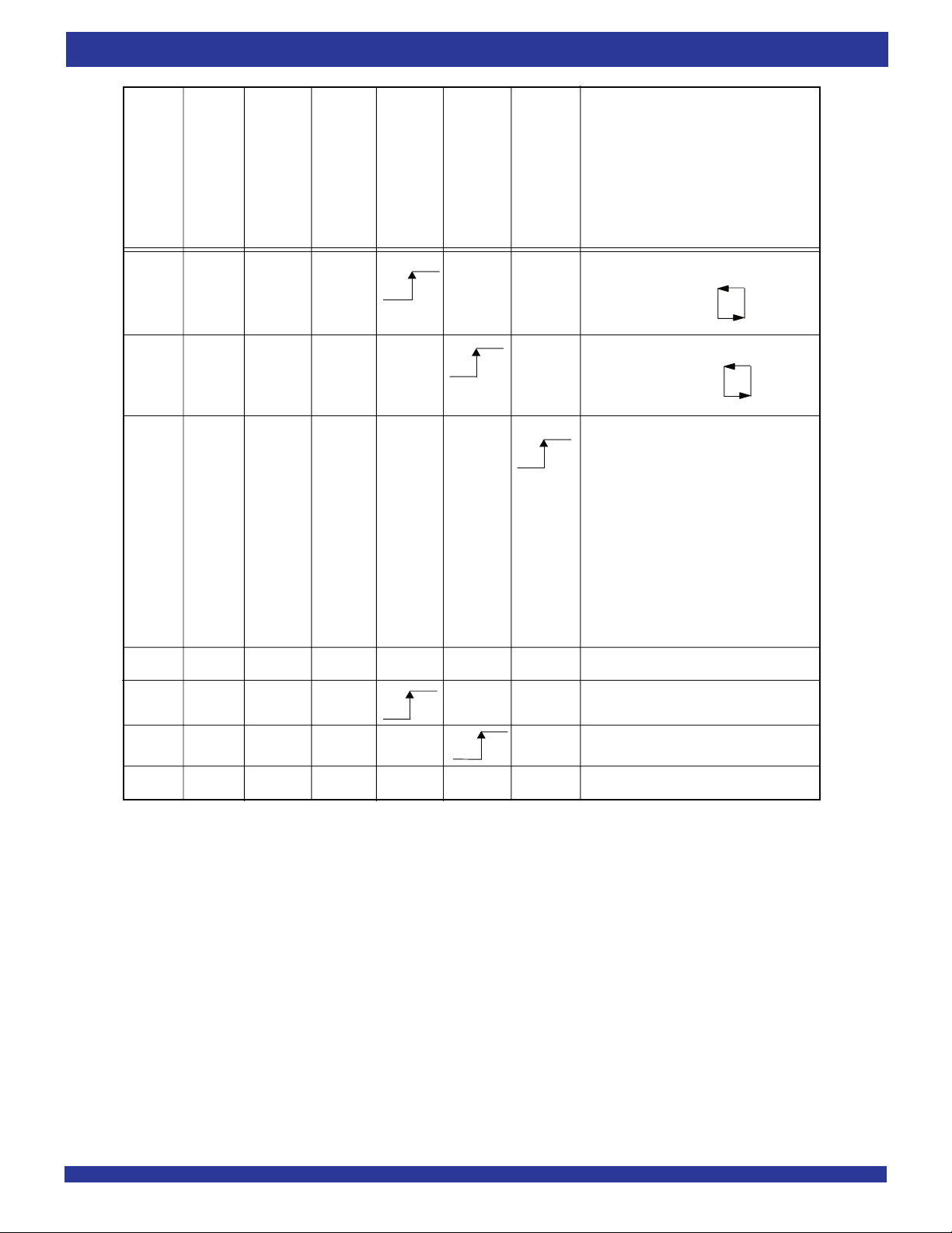
TABLE 2 — DEFAULT PROGRAMMABLE
FLAG OFFSETS
IDT72V7230, 72V7240
LD FSEL1 FSEL0 Offsets n,m
LH L511
L L H 255
L L L 127
LHH63
HL L31
HH L15
HLH7
HH H3
LD FSEL1 FSEL0 Program Mode
H X X Serial
L X X Parallel
IDT72V7250, 72V7260, 72V7270, 72V7280
LD FSEL1 FSEL0 Offsets n,m
H L L 1,023
LH L511
L L H 255
L L L 127
LHH63
HH L31
HLH15
HH H7
LD FSEL1 FSEL0 Program Mode
H X X Serial
L X X Parallel
IDT72V7290, 72V72100
LD FSEL1 FSEL0 Offsets n,m
L H L 16,383
L L H 8,191
L H H 4,095
H H L 2,047
H L L 1,023
HLH511
HHH255
LLL127
(3)
(4)
(3)
(4)
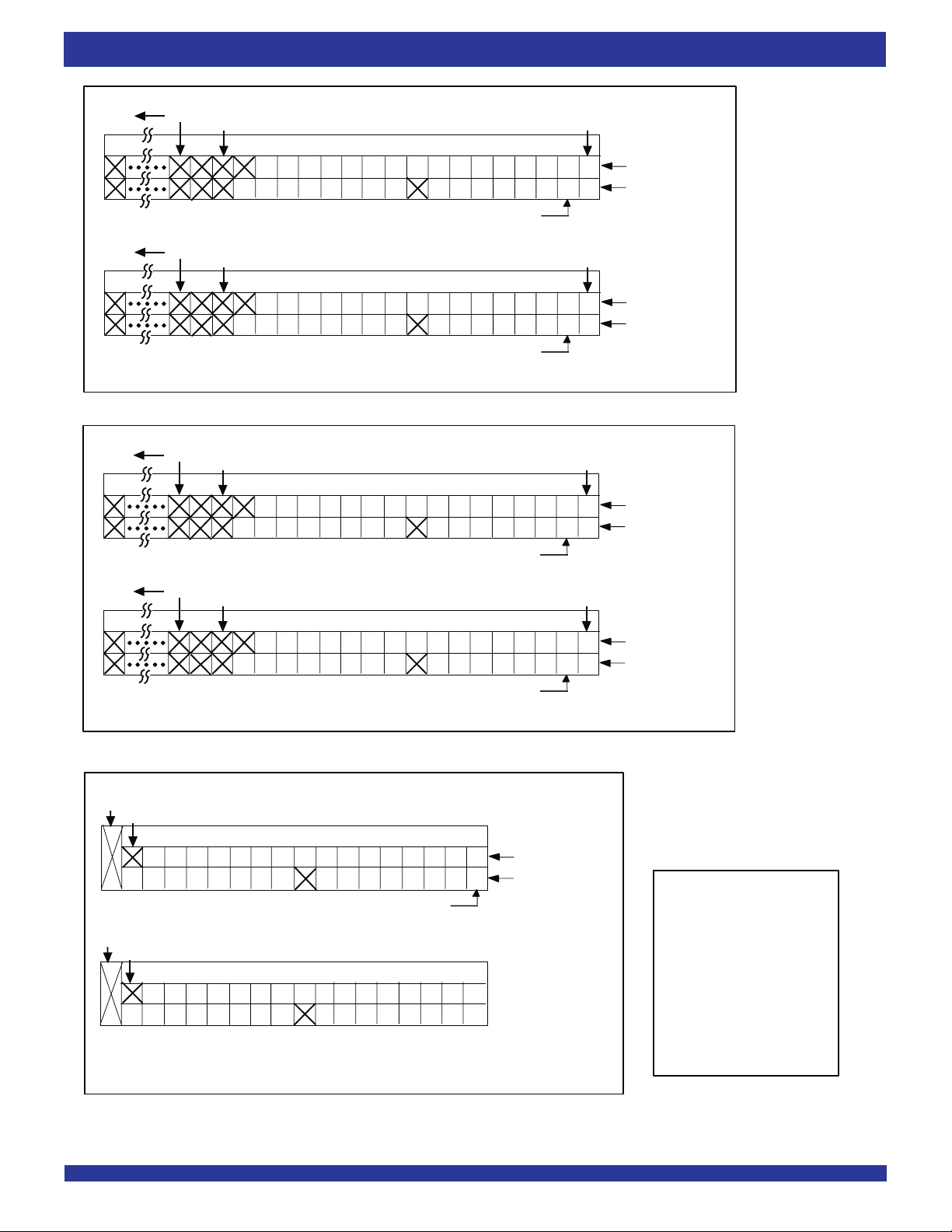
PROGRAMMING FLAG OFFSETS
Full and Empty Flag offset values are user programmable. The IDT72V7230/
72V7240/72V7250/72V7260/72V7270/72V7280/72V7290/72V72100 have
internal registers for these offsets. There are eight default offset values selectable
during Master Reset. These offset values are shown in Table 2. Offset values
can also be programmed into the FIFO in one of two ways; serial or parallel
loading method. The selection of the loading method is done using the LD (Load)
pin. During Master Reset, the state of the LD input determines whether serial
or parallel flag offset programming is enabled. A HIGH on LD during Master
Reset selects serial loading of offset values. A LOW on LD during Master Reset
selects parallel loading of offset values.
In addition to loading offset values into the FIFO, it is also possible to read
the current offset values. Offset values can be read via the parallel output port
Q
0-Qn, regardless of the programming mode selected (serial or parallel). It is
not possible to read the offset values in serial fashion.
Figure 3, Programmable Flag Offset Programming Sequence, summaries
the control pins and sequence for both serial and parallel programming modes.
For a more detailed description, see discussion that follows.
The offset registers may be programmed (and reprogrammed) any time after
Master Reset, regardless of whether serial or parallel programming has been
selected. Valid programming ranges are from 0 to D-1.
SYNCHRONOUS vs ASYNCHRONOUS PROGRAMMABLE FLAG
TIMING SELECTION
The IDT72V7230/72V7240/72V7250/72V7260/72V7270/72V7280/
72V7290/72V72100 can be configured during the Master Reset cycle with
either synchronous or asynchronous timing for PAF and PAE flags by use of
the PFM pin.
If synchronous PAF/PAE configuration is selected (PFM, HIGH during
MRS), the PAF is asserted and updated on the rising edge of WCLK only and
not RCLK. Similarly, PAE is asserted and updated on the rising edge of RCLK
only and not WCLK. For detail timing diagrams, see Figure 23 for synchronous
PAF timing and Figure 24 for synchronous PAE timing.
If asynchronous PAF/PAE configuration is selected (PFM, LOW during
MRS), the PAF is asserted LOW on the LOW-to-HIGH transition of WCLK and
PAF is reset to HIGH on the LOW-to-HIGH transition of RCLK. Similarly, PAE
is asserted LOW on the LOW-to-HIGH transition of RCLK. PAE is reset to HIGH
on the LOW-to-HIGH transition of WCLK. For detail timing diagrams, see Figure
25 for asynchronous PAF timing and Figure 26 for asynchronous PAE timing.
LD FSEL1 FSEL0 Program Mode
H X X Serial
L X X Parallel
NOTES:
1. n = empty offset for PAE.
2. m = full offset for PAF.
3. As well as selecting serial programming mode, one of the default values will also
be loaded depending on the state of FSEL0 & FSEL1.
4. As well as selecting parallel programming mode, one of the default values will
also be loaded depending on the state of FSEL0 & FSEL1.
(3)
(4)
10
IDT72V7230/7240/7250/7260/7270/7280/7290/72100 3.3V HIGH DENSITY SUPERSYNC IITM FIFO
512 x 72, 1K x 72, 2K x 72, 4K x 72, 8K x 36, 16K x 72, 32K x 72, 64K x 72
COMMERCIAL TEMPERATURE RANGE
H
PAE EF
HL L
HL
HF
HH
HH
FF PAF
(1)
0
1 to n
IDT72V7260
(1)
0
1 to n
HH
H
LHH
LHH
L
HH
(n+1) to 2,048
(n+1) to 1,024
LL
HHLH H
H
4,096
(4,096-m) to 4,095
2,049 to (4,096-(m+1))
to 2,047
2,048
(2048-m)
1,025 to (2048-(m+1))
H
PAE EF
HL L
HL
HF
HH
HH
FF PAF
(1)
0
1 to n
IDT72V72100
(1)
1 to n
IDT72V7290
HH
LH H
H
HH
(n+1) to 32,768
LH H
L
LL
HHLH H
H
to 65,535
65,536
(65,536-m)
32,769 to (65,536-(m+1))
(32,768-m) to 32,767
16,385 to (32,768-(m+1))
L
PAE OR
HF
IR PAF
IDT72V7250 IDT72V7260IDT72V7230
HL
LH L
HL H
HL
H
LH
LH
LH
1 to n+1
00
1 to n+1
(n+2) to 1,025 (n+2) to 2,049
LH L
L
HL
LHLHL
L
to 4,096
(4,097-m)
2,049 4,097
(2,049-m) to 2,048
1,026 to (2,049-(m+1)) 2,050 to (4,097-(m+1))
L
PAE OR
HL H
HL
HF
IR PAF
H
LH
LH
0
1 to n+1
1 to n+1
IDT72V7290 IDT72V72100
HL
LH
(n+2) to 32,769
4680 drw 05
LHL
LHL
L
L
HL
LHLH L
65,537
(65,537-m) to 65,536
32,770 to (65,537-(m+1))
to 32,768
(32,769-m)
16,386 to (32,769-(m+1))
1)
(1)
0
1 to n
(1)
0
1 to n
Number of
(n+1) to 512
(n+1) to 256
Words in
IDT72V7240 IDT72V7250
IDT72V7230
TABLE 3 STATUS FLAGS FOR IDT STANDARD MODE
1,024
(1024-m) to 1,023
513 to (1,024-(m+1))
512
(512-m) to 511
257 to (512-(m+1))
FIFO
(
00
1 to n
(1)
0
1 to n
IDT72V7270 IDT72V7280
Number of
to 16,383
(n+1) to 8,192 (n+1) to 16,384
(16,384-m)
8,193 to (16,384-(m+1))
to 8,191
(n+1) to 4,096
(8,192-m)
4,097 to (8,192-(m+1))
Words in
FIFO
16,384 32,768
8,192
NOTE:
1. See table 2 for values for n, m.
0
1 to n+1
IDT72V7240
0
1 to n+1
TABLE 4 STATUS FLAGS FOR FWFT MODE
Number of
to 1,024
(n+2) to 513
(1,025-m)
514 to (1,025-(m+1))
to 512
(n+2) to 257
(513-m)
258 to (513-(m+1))
Words in
FIFO
1,025
513
00
1 to n+1
0
1 to n+1
IDT72V7270 IDT72V7280
Number of
Words in
to 16,384
16,385 32,769
(n+2) to 8,193 (n+2) to 16,385
(16,385-m)
8,194 to (16,385-(m+1))
to 8,192
8,193
(n+2) to 4,097
(8,193-m)
4,098 to (8,193-(m+1))
FIFO
NOTE:
1. See table 2 for values for n, m.
11
IDT72V7230/7240/7250/7260/7270/7280/7290/72100 3.3V HIGH DENSITY SUPERSYNC IITM FIFO
512 x 72, 1K x 72, 2K x 72, 4K x 72, 8K x 36, 16K x 72, 32K x 72, 64K x 72
LD
WEN
REN
SEN
WCLK RCLK
SCLK
COMMERCIAL TEMPERATURE RANGE
IDT72V7230
IDT72V7240
IDT72V7250
IDT72V7260
IDT72V7270
IDT72V7280
IDT72V7290
IDT72V72100
0
0
1
1
X
X
Parallel write to registers:
Empty Offset
Full Offset
0
1
0
1
X
X
Parallel read from registers:
Empty Offset
Full Offset
Serial shift into registers:
0
1
1X
0
X
18 bits for the IDT72V7230
20 bits for the IDT72V7240
22 bits for the IDT72V7250
24 bits for the IDT72V7260
26 bits for the IDT72V7270
28 bits for the IDT72V7280
30 bits for the IDT72V7290
32 bits for the IDT72V72100
1 bit for each rising WCLK edge
Starting with Empty Offset (LSB)
Ending with Full Offset (MSB)
X
1
1
0
1
X
1
X
XX
X
X
X
No Operation
Write Memory
1
1
NOTES:
1. The programming method can only be selected at Master Reset.
2. Parallel reading of the offset registers is always permitted regardless of which programming method has been selected.
3. The programming sequence applies to both IDT Standard and FWFT modes.
X
1
0
1
X
X
Figure 3. Programmable Flag Offset Programming Sequence
X
XX
12
X
X
Read Memory
No Operation
4680 drw06
IDT72V7230/7240/7250/7260/7270/7280/7290/72100 3.3V HIGH DENSITY SUPERSYNC IITM FIFO
512 x 72, 1K x 72, 2K x 72, 4K x 72, 8K x 36, 16K x 72, 32K x 72, 64K x 72
COMMERCIAL TEMPERATURE RANGE
D/Q71 D/Q19
D/Q71 D/Q19
D/Q35 D/Q19
1st Parallel Offset Write/Read Cycle
D/Q17
D/Q8
EMPTY OFFSET REGISTER (PAE)
16
16
15
1415
14
11
10
9
910111213
2nd Parallel Offset Write/Read Cycle
D/Q17
D/Q8
FULL OFFSET REGISTER (PAF)
11
10
9
910111213
16
16
15
1415
14
x72 Bus Width
1st Parallel Offset Write/Read Cycle
D/Q17
EMPTY OFFSET REGISTER (PAE)
16
1415
14
15
16
11
10
910111213
D/Q8
9
8
# of Bits Used
8
# of Bits Used
8
# of Bits Used
D/Q0
Non-Interspersed
56781213
67
5
56781213
67
5
56781213
67
5
234
234
D/Q0
234
234
D/Q0
234
234
1
1
1
1
1
1
Parity
Interspersed
Parity
Non-Interspersed
Parity
Interspersed
Parity
Non-Interspersed
Parity
Interspersed
Parity
D/Q35 D/Q19
D/Q17
FULL OFFSET REGISTER (PAF)
2nd Parallel Offset Write/Read Cycle
16
1415
14
15
16
1st Parallel Offset Write/Read Cycle
D/Q17
Data Inputs/Outputs
EMPTY OFFSET (LSB) REGISTER (PAE)
16
16
1415
10
1213
11
9
D/Q8
2nd Parallel Offset Write/Read Cycle
D/Q17
D/Q16
Data Inputs/Outputs
FULL OFFSET (LSB) REGISTER (PAF)
13
1112
1011121314
9
D/Q8
16
141516
15
x18 Bus Width
D/Q8
11
10
9
8
910111213
x36 Bus Width
56789101112131415
5678
# of Bits Used
2345678
56781213
67
5
# of Bits Used
D/Q0D/Q16
Non-Interspersed
Parity
1234
Interspersed
1234
Parity
D/Q0
12345678910
1
234
234
D/Q0
1
1
Non-Interspersed
Parity
Interspersed
Parity
# of Bits Used:
09 bits for the IDT72V7230
10 bits for the IDT72V7240
11 bits for the IDT72V7250
12 bits for the IDT72V7260
13 bits for the IDT72V7270
14 bits for the IDT72V7280
15 bits for the IDT72V7290
16 bits for the IDT72V72100
Note: All unused input bits
are don’t care.
4680 drw07
Figure 3. Programmable Flag Offset Programming Sequence (Continued)
13

IDT72V7230/7240/7250/7260/7270/7280/7290/72100 3.3V HIGH DENSITY SUPERSYNC IITM FIFO
512 x 72, 1K x 72, 2K x 72, 4K x 72, 8K x 36, 16K x 72, 32K x 72, 64K x 72
COMMERCIAL TEMPERATURE RANGE
FUNCTIONAL DESCRIPTION
(CONTINUED)
SERIAL PROGRAMMING MODE
If Serial Programming mode has been selected, as described above, then
programming of PAE and PAF values can be achieved by using a combination
of the LD, SEN, SCLK and SI input pins. Programming PAE and PAF proceeds
as follows: when LD and SEN are set LOW, data on the SI input are written, one
bit for each SCLK rising edge, starting with the Empty Offset LSB and ending
with the Full Offset MSB. A total of 18 bits for the IDT72V7230, 20 bits for the
IDT72V7240, 22 bits for the IDT72V7250, 24 bits for the IDT72V7260, 26 bits
for the IDT72V7270, 28 bits for the IDT72V7280, 30 bits for the IDT72V7290
and 32 bits for the IDT72V72100. See Figure 20, Serial Loading of
Programmable Flag Registers, for the timing diagram for this mode.
Using the serial method, individual registers cannot be programmed
selectively. PAE and PAF can show a valid status only after the complete set
of bits (for all offset registers) has been entered. The registers can be
reprogrammed as long as the complete set of new offset bits is entered. When
LD is LOW and SEN is HIGH, no serial write to the registers can occur.
Write operations to the FIFO are allowed before and during the serial
programming sequence. In this case, the programming of all offset bits does not
have to occur at once. A select number of bits can be written to the SI input and
then, by bringing LD and SEN HIGH, data can be written to FIFO memory via
Dn by toggling WEN. When WEN is brought HIGH with LD and SEN restored
to a LOW, the next offset bit in sequence is written to the registers via SI. If an
interruption of serial programming is desired, it is sufficient either to set LD LOW
and deactivate SEN or to set SEN LOW and deactivate LD. Once LD and SEN
are both restored to a LOW level, serial offset programming continues.
From the time serial programming has begun, neither programmable flag
will be valid until the full set of bits required to fill all the offset registers has been
written. Measuring from the rising SCLK edge that achieves the above criteria;
PAF will be valid after three more rising WCLK edges plus tPAF, PAE will be valid
after the next three rising RCLK edges plus tPAE.
It is only possible to read the flag offset values via the parallel output port Qn.
PARALLEL MODE
If Parallel Programming mode has been selected, as described above, then
programming of PAE and PAF values can be achieved by using a combination
of the LD, WCLK, WEN and Dn input pins. Programming PAE and PAF
proceeds as follows: LD and WEN must be set LOW. For x72, x36 or x18 bit
input bus widths, data on the inputs Dn are written into the Empty Offset Register
on the first LOW-to-HIGH transition of WCLK. Upon the second LOW-to-HIGH
transition of WCLK, data are written into the Full Offset Register. The third
transition of WCLK writes, once again, to the Empty Offset Register. See Figure
3, Programmable Flag Offset Programming Sequence. See Figure 21,
Parallel Loading of Programmable Flag Registers, for the timing diagram for
this mode.
The act of writing offsets in parallel employs a dedicated write offset register
pointer. The act of reading offsets employs a dedicated read offset register
pointer. The two pointers operate independently; however, a read and a write
should not be performed simultaneously to the offset registers. A Master Reset
initializes both pointers to the Empty Offset register. A Partial Reset has no effect
on the position of these pointers.
Write operations to the FIFO are allowed before and during the parallel
programming sequence. In this case, the programming of all offset registers does
not have to occur at one time. One offset register can be written and then by
bringing LD HIGH, write operations can be redirected to the FIFO memory.
When LD is set LOW again, and WEN is LOW, the next offset register in sequence
is written to. As an alternative to holding WEN LOW and toggling LD, parallel
programming can also be interrupted by setting LD LOW and toggling WEN.
Note that the status of a programmable flag (PAE or PAF) output is invalid
during the programming process. From the time parallel programming has
begun, a programmable flag output will not be valid until the appropriate offset
word has been written to the register pertaining to that flag. Measuring from the
rising WCLK edge that achieves the above criteria; PAF will be valid after two
more rising WCLK edges plus t
PAF, PAE will be valid after the next two rising
RCLK edges plus tPAE plus tSKEW2.
The act of reading the offset registers employs a dedicated read offset
register pointer. The contents of the offset registers can be read on the Q
0-Q16
pins when LD is set LOW and REN is set LOW. For x72, x36 or x18 output bus
width, data are read via Q0-Q16 from the Empty Offset Register on the first
LOW-to-HIGH transition of RCLK. Upon the second LOW-to-HIGH transition
of RCLK, data are read from the Full Offset Register. The third transition of RCLK
reads, once again, from the Empty Offset Register. See Figure 3, Program-
mable Flag Offset Programming Sequence. See Figure 22, Parallel Read of
Programmable Flag Registers, for the timing diagram for this mode.
It is permissible to interrupt the offset register read sequence with reads or
writes to the FIFO. The interruption is accomplished by deasserting REN, LD,
or both together. When REN and LD are restored to a LOW level, reading of
the offset registers continues where it left off. It should be noted, and care should
be taken from the fact that when a parallel read of the flag offsets is performed,
the data word that was present on the output lines Qn will be overwritten.
Parallel reading of the offset registers is always permitted regardless of
which timing mode (IDT Standard or FWFT modes) has been selected.
RETRANSMIT OPERATION
The Retransmit operation allows data that has already been read to be
accessed again. There are 2 modes of Retransmit operation, normal latency
and zero latency. There are two stages to Retransmit: first, a setup procedure
that resets the read pointer to the first location of memory, then the actual
retransmit, which consists of reading out the memory contents, starting at the
beginning of memory.
Retransmit setup is initiated by holding RT LOW during a rising RCLK edge.
REN and WEN must be HIGH before bringing RT LOW. When zero latency is
utilized, REN does not need to be HIGH before bringing RT LOW. At least two words,
but no more than D - 2 words should have been written into the FIFO, and read
from the FIFO, between Reset (Master or Partial) and the time of Retransmit
setup. D = 512 for the IDT72V7230, 1,024 for the IDT72V7240, 2,048 for the
IDT72V7250, 4,096 for the IDT72V7260, 8,192 for the IDT72V7270, 16,384
for the IDT72V7280, 32,768 for the IDT72V7290 and 65,536 for the
IDT72V72100. In FWFT mode, D = 513 for the IDT72V7230, 1,025 for the
IDT72V7240, 2,049 for the IDT72V7250, 4,097 for the IDT72V7260, 8,193 for
the IDT72V7270, 16,385 for the IDT72V7280, 32,769 for the IDT72V7290 and
65,537 for the IDT72V72100.
If IDT Standard mode is selected, the FIFO will mark the beginning of the
Retransmit setup by setting EF LOW. The change in level will only be noticeable
if EF was HIGH before setup. During this period, the internal read pointer is
initialized to the first location of the RAM array.
When EF goes HIGH, Retransmit setup is complete and read operations
may begin starting with the first location in memory. Since IDT Standard mode
is selected, every word read including the first word following Retransmit setup
requires a LOW on REN to enable the rising edge of RCLK. See Figure 16,
Retransmit Timing (IDT Standard Mode), for the relevant timing diagram.
14

IDT72V7230/7240/7250/7260/7270/7280/7290/72100 3.3V HIGH DENSITY SUPERSYNC IITM FIFO
512 x 72, 1K x 72, 2K x 72, 4K x 72, 8K x 36, 16K x 72, 32K x 72, 64K x 72
COMMERCIAL TEMPERATURE RANGE
If FWFT mode is selected, the FIFO will mark the beginning of the Retransmit
setup by setting OR HIGH. During this period, the internal read pointer is set
to the first location of the RAM array.
When OR goes LOW, Retransmit setup is complete; at the same time, the
contents of the first location appear on the outputs. Since FWFT mode is selected,
the first word appears on the outputs, no LOW on REN is necessary. Reading
all subsequent words requires a LOW on REN to enable the rising edge of
RCLK. See Figure 17, Retransmit Timing (FWFT Mode), for the relevant timing
diagram.
For either IDT Standard mode or FWFT mode, updating of the PAE, HF
and PAF flags begin with the rising edge of RCLK that RT is setup. PAE is
synchronized to RCLK, thus on the second rising edge of RCLK after RT is setup,
the PAE flag will be updated. HF is asynchronous, thus the rising edge of RCLK
that RT is setup will update HF. PAF is synchronized to WCLK, thus the second
rising edge of WCLK that occurs t
SKEW after the rising edge of RCLK that RT
is setup will update PAF. RT is synchronized to RCLK.
The Retransmit function has the option of two modes of operation, either
“normal latency” or “zero latency”. Figure 16 and Figure 17 mentioned
previously, relate to “normal latency”. Figure 18 and Figure 19 show “zero
latency” retransmit operation. Zero latency basically means that the first data
word to be retransmitted, is placed onto the output register with respect to the
RCLK pulse that initiated the retransmit.
15

IDT72V7230/7240/7250/7260/7270/7280/7290/72100 3.3V HIGH DENSITY SUPERSYNC IITM FIFO
512 x 72, 1K x 72, 2K x 72, 4K x 72, 8K x 36, 16K x 72, 32K x 72, 64K x 72
COMMERCIAL TEMPERATURE RANGE
SIGNAL DESCRIPTION
INPUTS:
DATA IN (D0 - Dn)
Data inputs for 72-bit wide data (D0 - D71), data inputs for 36-bit wide data
(D0 - D35) or data inputs for 18-bit wide data (D0 - D17).
CONTROLS:
MASTER RESET ( MRS )
A Master Reset is accomplished whenever the MRS input is taken to a LOW
state. This operation sets the internal read and write pointers to the first location
of the RAM array. PAE will go LOW, PAF will go HIGH, and HF will go HIGH.
If FWFT/SI is LOW during Master Reset then the IDT Standard mode,
along with EF and FF are selected. EF will go LOW and FF will go HIGH. If
FWFT/SI is HIGH, then the First Word Fall Through mode (FWFT), along with
IR and OR, are selected. OR will go HIGH and IR will go LOW.
All control settings such as OW, IW, BM, BE, RM, PFM and IP are defined
during the Master Reset cycle.
During a Master Reset, the output register is initialized to all zeroes. A Master
Reset is required after power up, before a write operation can take place. MRS
is asynchronous.
See Figure 8, Master Reset Timing, for the relevant timing diagram.
PARTIAL RESET ( PRS )
A Partial Reset is accomplished whenever the PRS input is taken to a LOW
state. As in the case of the Master Reset, the internal read and write pointers
are set to the first location of the RAM array, PAE goes LOW, PAF goes HIGH,
and HF goes HIGH.
Whichever mode is active at the time of Partial Reset, IDT Standard mode
or First Word Fall Through, that mode will remain selected. If the IDT Standard
mode is active, then FF will go HIGH and EF will go LOW. If the First Word Fall
Through mode is active, then OR will go HIGH, and IR will go LOW.
Following Partial Reset, all values held in the offset registers remain
unchanged. The programming method (parallel or serial) currently active at
the time of Partial Reset is also retained. The output register is initialized to all
zeroes. PRS is asynchronous.
A Partial Reset is useful for resetting the device during the course of
operation, when reprogramming programmable flag offset settings may not be
convenient.
See Figure 9, Partial Reset Timing, for the relevant timing diagram.
RETRANSMIT ( RT )
The Retransmit operation allows data that has already been read to be
accessed again. There are 2 modes of Retransmit operation, normal latency
and zero latency. There are two stages to Retransmit: first, a setup procedure
that resets the read pointer to the first location of memory, then the actual
retransmit, which consists of reading out the memory contents, starting at the
beginning of the memory.
Retransmit setup is initiated by holding RT LOW during a rising RCLK edge.
REN and WEN must be HIGH before bringing RT LOW. When zero latency is
utilized, REN does not need to be HIGH before bringing RT LOW.
If IDT Standard mode is selected, the FIFO will mark the beginning of the
Retransmit setup by setting EF LOW. The change in level will only be noticeable
if EF was HIGH before setup. During this period, the internal read pointer is
initialized to the first location of the RAM array.
When EF goes HIGH, Retransmit setup is complete and read operations
may begin starting with the first location in memory. Since IDT Standard mode
is selected, every word read including the first word following Retransmit setup
requires a LOW on REN to enable the rising edge of RCLK. See Figure 16,
Retransmit Timing (IDT Standard Mode), for the relevant timing diagram.
If FWFT mode is selected, the FIFO will mark the beginning of the Retransmit
setup by setting OR HIGH. During this period, the internal read pointer is set
to the first location of the RAM array.
When OR goes LOW, Retransmit setup is complete; at the same time, the
contents of the first location appear on the outputs. Since FWFT mode is selected,
the first word appears on the outputs, no LOW on REN is necessary. Reading
all subsequent words requires a LOW on REN to enable the rising edge of
RCLK. See Figure 17, Retransmit Timing (FWFT Mode), for the relevant timing
diagram.
In Retransmit operation, zero latency mode can be selected using the
Retransmit Mode (RM) pin during a Master Reset. This can be applied to both
IDT Standard mode and FWFT mode.
Note, the Read Chip Select (RCS) input must be LOW during Retransmit.
The RCS input enables/disables the REN input.
FIRST WORD FALL THROUGH/SERIAL IN (FWFT/SI)
This is a dual purpose pin. During Master Reset, the state of the FWFT/
SI input determines whether the device will operate in IDT Standard mode or
First Word Fall Through (FWFT) mode.
If, at the time of Master Reset, FWFT/SI is LOW, then IDT Standard mode
will be selected. This mode uses the Empty Flag (EF) to indicate whether or
not there are any words present in the FIFO memory. It also uses the Full Flag
function (FF) to indicate whether or not the FIFO memory has any free space
for writing. In IDT Standard mode, every word read from the FIFO, including
the first, must be requested using the Read Enable (REN) and RCLK.
If, at the time of Master Reset, FWFT/SI is HIGH, then FWFT mode will be
selected. This mode uses Output Ready (OR) to indicate whether or not there
is valid data at the data outputs (Q
whether or not the FIFO memory has any free space for writing. In the FWFT
mode, the first word written to an empty FIFO goes directly to Qn after three RCLK
rising edges, REN = LOW is not necessary. Subsequent words must be
accessed using the Read Enable (REN) and RCLK.
After Master Reset, FWFT/SI acts as a serial input for loading PAE and PAF
offsets into the programmable registers. The serial input function can only be
used when the serial loading method has been selected during Master Reset.
Serial programming using the FWFT/SI pin functions the same way in both IDT
Standard and FWFT modes.
WRITE CLOCK (WCLK)
A write cycle is initiated on the rising edge of the WCLK input. Data setup
and hold times must be met with respect to the LOW-to-HIGH transition of the
WCLK. It is permissible to stop the WCLK. Note that while WCLK is idle, the FF/
IR, PAF and HF flags will not be updated. (Note that WCLK is only capable of
updating HF flag to LOW.) The Write and Read Clocks can either be
independent or coincident.
WRITE ENABLE ( WEN )
When the WEN input is LOW, data may be loaded into the FIFO RAM array
on the rising edge of every WCLK cycle if the device is not full. Data is stored
in the RAM array sequentially and independently of any ongoing read
operation.
When WEN is HIGH, no new data is written in the RAM array on each WCLK
cycle.
To prevent data overflow in the IDT Standard mode, FF will go LOW,
inhibiting further write operations. Upon the completion of a valid read cycle,
n). It also uses Input Ready (IR) to indicate
16

IDT72V7230/7240/7250/7260/7270/7280/7290/72100 3.3V HIGH DENSITY SUPERSYNC IITM FIFO
512 x 72, 1K x 72, 2K x 72, 4K x 72, 8K x 36, 16K x 72, 32K x 72, 64K x 72
COMMERCIAL TEMPERATURE RANGE
FF will go HIGH allowing a write to occur. The FF is updated by two WCLK
cycles + tSKEW after the RCLK cycle.
To prevent data overflow in the FWFT mode, IR will go HIGH, inhibiting
further write operations. Upon the completion of a valid read cycle, IR will go
LOW allowing a write to occur. The IR flag is updated by two WCLK cycles +
tSKEW after the valid RCLK cycle.
WEN is ignored when the FIFO is full in either FWFT or IDT Standard mode.
READ CLOCK (RCLK)
A read cycle is initiated on the rising edge of the RCLK input. Data can be
read on the outputs, on the rising edge of the RCLK input. It is permissible to
stop the RCLK. Note that while RCLK is idle, the EF/OR, PAE and HF flags will
not be updated. (Note that RCLK is only capable of updating the HF flag to
HIGH.) The Write and Read Clocks can be independent or coincident.
READ ENABLE ( REN )
When Read Enable is LOW, data is loaded from the RAM array into the output
register on the rising edge of every RCLK cycle if the device is not empty.
When the REN input is HIGH, the output register holds the previous data
and no new data is loaded into the output register. The data outputs Q0-Qn
maintain the previous data value.
In the IDT Standard mode, every word accessed at Qn, including the first
word written to an empty FIFO, must be requested using REN provided that RCS
is LOW. When the last word has been read from the FIFO, the Empty Flag (EF)
will go LOW, inhibiting further read operations. REN is ignored when the FIFO
is empty. Once a write is performed, EF will go HIGH allowing a read to occur.
The EF flag is updated by two RCLK cycles + tSKEW after the valid WCLK cycle.
In the FWFT mode, the first word written to an empty FIFO automatically goes
to the outputs Qn, on the third valid LOW-to-HIGH transition of RCLK + tSKEW
after the first write. REN and RCS do not need to be asserted LOW. In order
to access all other words, a read must be executed using REN and RCS must
be enabled LOW. The RCLK LOW-to-HIGH transition after the last word has
been read from the FIFO, Output Ready (OR) will go HIGH with a true read
(RCLK with REN = LOW; RCS = LOW), inhibiting further read operations. REN
is ignored when the FIFO is empty.
SERIAL CLOCK ( SCLK )
During serial loading of the programmable flag offset registers, a rising edge
on the SCLK input is used to load serial data present on the SI input provided
that the SEN input is LOW.
READ CHIP SELECT ( RCS )
The Read Chip Select input provides synchronous control of the Read
output port. When RCS goes LOW, the next rising edge of RCLK causes the
Qn outputs to go to the LOW Z state. When RCS goes HIGH, the next RCLK
rising edge causes the Qn outputs to return to HIGH Z. During a Master or Partial
Reset the RCS input can be HIGH or LOW. OE provides High-Impedance
control of the data outputs. If OE is LOW the data outputs will be Low-Impedance
regardless of RCS until the first rising edge of RCLK after reset is complete. Then
if RCS is HIGH the data outputs will go to High-Impedance.
During the time while RCS is HIGH (disabled) all read operations are
ignored. That is, the REN input is disabled and data is not clocked from the RAM
array to the output register.
The RCS input does not effect the operation of the flags. For example, when
the first word is written to an empty FIFO, the EF will still go from LOW to HIGH
based on a rising edge of RCLK, regardless of the state of the RCS input.
Also, when operating the FIFO in FWFT mode the first word written to an
empty FIFO will still be clocked through to the output register based on RCLK,
regardless of the state of RCS. The RCS pin must also be active (LOW) in order
to perform a Retransmit. See figure 12 for Read Cycle and Read Chip Select
Timing (IDT Standard Mode). See figure 15 for Read Cycle and Read Chip
Select Timing (First Word Fall Through Mode).
LOAD ( LD )
This is a dual purpose pin. During Master Reset, the state of the LD input,
along with FSEL0 and FSEL1, determines one of eight default offset values for
the PAE and PAF flags, along with the method by which these offset registers
can be programmed, parallel or serial (see Table 2). After Master Reset, LD
enables write operations to and read operations from the offset registers. Only
the offset loading method currently selected can be used to write to the registers.
Offset registers can be read only in parallel.
After Master Reset, the LD pin is used to activate the programming process
of the flag offset values PAE and PAF. Pulling LD LOW will begin a serial loading
or parallel load or read of these offset values.
BUS-MATCHING (BM, IW, OW)
The pins BM, IW and OW are used to define the input and output bus widths.
During Master Reset, the state of these pins is used to configure the device bus
sizes. See Table 1 for control settings. All flags will operate on the word/byte
size boundary as defined by the selection of bus width. See Figure 4 for Bus-
Matching Byte Arrangement.
SERIAL ENABLE ( SEN )
The SEN input is an enable used only for serial programming of the offset
registers. The serial programming method must be selected during Master
Reset. SEN is always used in conjunction with LD. When these lines are both
LOW, data at the SI input can be loaded into the program register one bit for each
LOW-to-HIGH transition of SCLK.
When SEN is HIGH, the programmable registers retains the previous
settings and no offsets are loaded. SEN functions the same way in both IDT
Standard and FWFT modes.
OUTPUT ENABLE ( OE )
When Output Enable is enabled (LOW), the parallel output buffers receive
data from the output register. When OE is HIGH, the output data bus (Qn) goes
into a high impedance state. Note, during a Master or Partial Reset RCS can
be HIGH or LOW, OE is the only input that can place the output bus into HighImpedance.
BIG-ENDIAN/LITTLE-ENDIAN ( BE )
During Master Reset, a LOW on BE will select Big-Endian operation. A
HIGH on BE during Master Reset will select Little-Endian format. This function
is useful when the following input to output bus widths are implemented: x72 to
x36, x72 to x18, x36 to x72 and x18 to x72. If Big-Endian mode is selected,
then the most significant byte (word) of the long word written into the FIFO will
be read out of the FIFO first, followed by the least significant long word. If LittleEndian format is selected, then the least significant word of the long word written
into the FIFO will be read out first, followed by the most significant word. The
mode desired is configured during master reset by the state of the Big-Endian
(BE) pin. See Figure 4 for Bus-Matching Byte Arrangement.
PROGRAMMABLE FLAG MODE (PFM)
During Master Reset, a LOW on PFM will select Asynchronous Programmable flag timing mode. A HIGH on PFM will select Synchronous Programmable
17

IDT72V7230/7240/7250/7260/7270/7280/7290/72100 3.3V HIGH DENSITY SUPERSYNC IITM FIFO
512 x 72, 1K x 72, 2K x 72, 4K x 72, 8K x 36, 16K x 72, 32K x 72, 64K x 72
COMMERCIAL TEMPERATURE RANGE
flag timing mode. If asynchronous PAF/PAE configuration is selected (PFM,
LOW during MRS), the PAE is asserted LOW on the LOW-to-HIGH transition
of RCLK. PAE is reset to HIGH on the LOW-to-HIGH transition of WCLK.
Similarly, the PAF is asserted LOW on the LOW-to-HIGH transition of WCLK and
PAF is reset to HIGH on the LOW-to-HIGH transition of RCLK.
If synchronous PAE/PAF configuration is selected (PFM, HIGH during
MRS) , the PAE is asserted and updated on the rising edge of RCLK only and
not WCLK. Similarly, PAF is asserted and updated on the rising edge of WCLK
only and not RCLK. The mode desired is configured during master reset by
the state of the Programmable Flag Mode (PFM) pin.
INTERSPERSED PARITY (IP)
During Master Reset, a LOW on IP will select Non-Interspersed Parity mode.
A HIGH will select Interspersed Parity mode. The IP bit function allows the user
to select the parity bit in the long word loaded into the parallel port (D0-Dn) when
programming the flag offsets. If Interspersed Parity mode is selected, then the
FIFO will assume that the parity bits are located in bit position D8, D17, D26, D35,
D44, D53, D62 and D71 during the parallel programming of the flag offsets. If
Non-Interspersed Parity mode is selected, then D
to be valid bits and D
64, D65, D66, D67, D68, D69, D70 and D71 are ignored.
8, D17 and D28 are is assumed
IP mode is selected during Master Reset by the state of the IP input pin.
OUTPUTS:
FULL FLAG ( FF/IR )
This is a dual purpose pin. In IDT Standard mode, the Full Flag (FF) function
is selected. When the FIFO is full, FF will go LOW, inhibiting further write
operations. When FF is HIGH, the FIFO is not full. If no reads are performed
after a reset (either MRS or PRS), FF will go LOW after D writes to the FIFO
(D = 512 for the IDT72V7230, 1,024 for the IDT72V7240, 2,048 for the
IDT72V7250, 4,096 for the IDT72V7260, 8,192 for the IDT72V7270, 16,384
for the IDT72V7280, 32,768 for the IDT72V7290 and 65,536 for the
IDT72V72100). See Figure10, Write Cycle and Full Flag Timing (IDT
Standard Mode), for the relevant timing information.
In FWFT mode, the Input Ready (IR) function is selected. IR goes LOW
when memory space is available for writing in data. When there is no longer
any free space left, IR goes HIGH, inhibiting further write operations. If no reads
are performed after a reset (either MRS or PRS), IR will go HIGH after D writes
to the FIFO (D = 513 for the IDT72V7230, 1,025 for the IDT72V7240, 2,049
for the IDT72V7250, 4,097 for the IDT72V7260, 8,193 for the IDT72V7270,
16,385 for the IDT72V7280, 32,769 for the IDT72V7290 and 65,537 for the
IDT72V72100). See Figure 13, Write Timing (FWFT Mode), for the relevant
timing information.
The IR status not only measures the contents of the FIFO memory, but also
counts the presence of a word in the output register. Thus, in FWFT mode, the
total number of writes necessary to deassert IR is one greater than needed to
assert FF in IDT Standard mode.
FF/IR is synchronous and updated on the rising edge of WCLK. FF/IR are
double register-buffered outputs.
EMPTY FLAG ( EF/OR )
This is a dual purpose pin. In the IDT Standard mode, the Empty Flag (EF)
function is selected. When the FIFO is empty, EF will go LOW, inhibiting further
read operations. When EF is HIGH, the FIFO is not empty. See Figure 11,
Read Cycle, Output Enable, Empty Flag and First Word Latency Timing (IDT
Standard Mode), for the relevant timing information.
In FWFT mode, the Output Ready (OR) function is selected. OR goes LOW
at the same time that the first word written to an empty FIFO appears valid on
the outputs. OR stays LOW after the RCLK LOW to HIGH transition that shifts
the last word from the FIFO memory to the outputs. OR goes HIGH only with
a true read (RCLK with REN = LOW). The previous data stays at the outputs,
indicating the last word was read. Further data reads are inhibited until OR goes
LOW again. See Figure 10, Read Timing (FWFT Mode), for the relevant timing
information.
EF/OR is synchronous and updated on the rising edge of RCLK.
In IDT Standard mode, EF is a double register-buffered output. In FWFT
mode, OR is a triple register-buffered output.
PROGRAMMABLE ALMOST-FULL FLAG ( PAF )
The Programmable Almost-Full flag (PAF) will go LOW when the FIFO
reaches the almost-full condition. In IDT Standard mode, if no reads are
performed after reset (MRS), PAF will go LOW after (D - m) words are written
to the FIFO. The PAF will go LOW after (512-m) writes for the IDT72V7230,
(1,024-m) writes for the IDT72V7240, (2,048-m) writes for the IDT72V7250,
(4,096-m) writes for the IDT72V7260, (8,192-m) writes for the IDT72V7270,
(16,384-m) writes for the IDT72V7280, (32,768-m) writes for the IDT72V7290,
and (65,536-m) writes for the IDT72V72100. The offset “m” is the full offset value.
The default setting for this value is stated in the footnote of Table 1.
In FWFT mode, the PAF will go LOW after (513-m) writes for the IDT72V7230,
(1,025-m) writes for the IDT72V7240, (2,049-m) writes for the IDT72V7250,
(4,097-m) writes for the IDT72V7260 and (8,193-m) writes for the IDT72V7270,
(16,385-m) writes for the IDT72V7280, (32,769-m) writes for the IDT72V7290
and (65,537-m) writes for the IDT72V72100, where “m” is the full offset value.
The default setting for this value is stated in Table 2.
See Figure 23, Synchronous Programmable Almost-Full Flag Timing (IDT
Standard and FWFT Modes), for the relevant timing information.
If asynchronous PAF configuration is selected, the PAF is asserted LOW
on the LOW-to-HIGH transition of the Write Clock (WCLK). PAF is reset to HIGH
on the LOW-to-HIGH transition of the Read Clock (RCLK). If synchronous PAF
configuration is selected, the PAF is updated on the rising edge of WCLK. See
Figure 25, Asynchronous Almost-Full Flag Timing (IDT Standard and FWFT
Modes).
PROGRAMMABLE ALMOST-EMPTY FLAG ( PAE )
The Programmable Almost-Empty flag (PAE) will go LOW when the FIFO
reaches the almost-empty condition. In IDT Standard mode, PAE will go LOW
when there are n words or less in the FIFO. The offset “n” is the empty offset
value. The default setting for this value is stated in the footnote of Table 1.
In FWFT mode, the PAE will go LOW when there are n+1 words or less
in the FIFO. The default setting for this value is stated in Table 2.
See Figure 24, Synchronous Programmable Almost-Empty Flag Timing
(IDT Standard and FWFT Modes), for the relevant timing information.
If asynchronous PAE configuration is selected, the PAE is asserted LOW
on the LOW-to-HIGH transition of the Read Clock (RCLK). PAE is reset to HIGH
on the LOW-to-HIGH transition of the Write Clock (WCLK). If synchronous PAE
configuration is selected, the PAE is updated on the rising edge of RCLK. See
Figure 26, Asynchronous Programmable Almost-Empty Flag Timing (IDT
Standard and FWFT Modes).
HALF-FULL FLAG ( HF )
This output indicates a half-full FIFO. The rising WCLK edge that fills the FIFO
beyond half-full sets HF LOW. The flag remains LOW until the difference between
the write and read pointers becomes less than or equal to half of the total depth
of the device; the rising RCLK edge that accomplishes this condition sets HF
HIGH.
18

IDT72V7230/7240/7250/7260/7270/7280/7290/72100 3.3V HIGH DENSITY SUPERSYNC IITM FIFO
512 x 72, 1K x 72, 2K x 72, 4K x 72, 8K x 36, 16K x 72, 32K x 72, 64K x 72
COMMERCIAL TEMPERATURE RANGE
In IDT Standard mode, if no reads are performed after reset (MRS or PRS),
HF will go LOW after (D/2 + 1) writes to the FIFO, where D = 512 for the
IDT72V7230, 1,024 for the IDT72V7240, 2,048 for the IDT72V7250, 4,096 for
the IDT72V7260, 8,192 for the IDT72V7270, 16,384 for the IDT72V7280,
32,768 for the IDT72V7290 and 65,536 for the IDT72V72100.
In FWFT mode, if no reads are performed after reset (MRS or PRS), HF
will go LOW after (D-1/2 + 2) writes to the FIFO, where D = 513 for the
IDT72V7230, 1,025 for the IDT72V7240, 2,049 for the IDT72V7250, 4,097 for
the IDT72V7260, 8,193 for the IDT72V7270, 16,385 for the IDT72V7280,
32,769 for the IDT72V7290 and 65,537 for the IDT72V72100.
See Figure 27, Half-Full Flag Timing (IDT Standard and FWFT Modes),
for the relevant timing information. Because HF is updated by both RCLK and
WCLK, it is considered asynchronous.
DATA OUTPUTS (Q
0-Qn)
(Q0-Q71) are data outputs for 72-bit wide data, (Q0 - Q35) are data outputs
for 36-bit wide data or (Q0-Q17) are data outputs for 18-bit wide data.
19

IDT72V7230/7240/7250/7260/7270/7280/7290/72100 3.3V HIGH DENSITY SUPERSYNC IITM FIFO
512 x 72, 1K x 72, 2K x 72, 4K x 72, 8K x 36, 16K x 72, 32K x 72, 64K x 72
COMMERCIAL TEMPERATURE RANGE
BYTE ORDER ON INPUT PORT:
BYTE ORDER ON OUTPUT PORT:
BE BM IW OW
X L X X
BE BM IW OW
L H L L
BE BM IW OW
H H L L
D71-D54 D53-D36 D35-D18 D17-D0
A
B
C
D
Q71-Q54 Q53-Q36 Q35-Q18 Q17-Q0
A
B
(a) x72 INPUT to x72 OUTPUT
C
D
Q71-Q54 Q53-Q36 Q35-Q18 Q17-Q0
A
B
Q71-Q54 Q53-Q36 Q35-Q18 Q17-Q0
C
(b) x72 INPUT to x36 OUTPUT - BIG-ENDIAN
D
Q71-Q54 Q53-Q36 Q35-Q18 Q17-Q0
C
D
Q71-Q54 Q53-Q36 Q35-Q18 Q17-Q0
A
(c) x72 INPUT to x36 OUTPUT - LITTLE-ENDIAN
B
Write to FIFO
Read from FIFO
1st: Read from FIFO
2nd: Read from FIFO
1st: Read from FIFO
2nd: Read from FIFO
BE BM IW OW
L H L H
BE BM IW OW
H H L H
Q71-Q54 Q53-Q36 Q35-Q18 Q17-Q0
A
Q71-Q54 Q53-Q36 Q35-Q18 Q17-Q0
B
Q71-Q54 Q53-Q36 Q35-Q18 Q17-Q0
C
Q71-Q54 Q53-Q36 Q35-Q18 Q17-Q0
D
(d) x72 INPUT to x18 OUTPUT - BIG-ENDIAN
Q71-Q54 Q53-Q36 Q35-Q18 Q17-Q0
D
Q71-Q54 Q53-Q36 Q35-Q18 Q17-Q0
C
Q71-Q54 Q53-Q36 Q35-Q18 Q17-Q0
B
Q71-Q54 Q53-Q36 Q35-Q18 Q17-Q0
A
1st: Read from FIFO
2nd: Read from FIFO
3rd: Read from FIFO
4th: Read from FIFO
1st: Read from FIFO
2nd: Read from FIFO
3rd: Read from FIFO
4th: Read from FIFO
(e) x72 INPUT to x18 OUTPUT - LITTLE-ENDIAN
Figure 4. Bus-Matching Byte Arrangement
20
4680 drw08

IDT72V7230/7240/7250/7260/7270/7280/7290/72100 3.3V HIGH DENSITY SUPERSYNC IITM FIFO
512 x 72, 1K x 72, 2K x 72, 4K x 72, 8K x 36, 16K x 72, 32K x 72, 64K x 72
COMMERCIAL TEMPERATURE RANGE
BYTE ORDER ON INPUT PORT:
BYTE ORDER ON OUTPUT PORT:
BE BM IW OW
L H H L
BE BM IW OW
H H H L
D71-D54 D53-D36 D35-D18 D17-D0
A
B
D71-D54 D53-D36 D35-D18 D17-D0
C
D
Q71-Q54 Q53-Q36 Q35-Q18 Q17-Q0
A
(a) x36 INPUT to x72 OUTPUT - BIG-ENDIAN
B
C
D
Q71-Q54 Q53-Q36 Q35-Q18 Q17-Q0
C
(b) x36 INPUT to x72 OUTPUT - LITTLE-ENDIAN
D
A
B
1st: Write to FIFO
2nd: Write to FIFO
Read from FIFO
Read from FIFO
BYTE ORDER ON INPUT PORT:
BYTE ORDER ON OUTPUT PORT:
BE BM IW OW
L H H H
Q71-Q54 Q53-Q36 Q35-Q18 Q17-Q0
A
Q71-Q54 Q53-Q36 Q35-Q18 Q17-Q0
B
Q71-Q54 Q53-Q36 Q35-Q18 Q17-Q0
C
Q71-Q54 Q53-Q36 Q35-Q18 Q17-Q0
D
Q71-Q54 Q53-Q36 Q35-Q18 Q17-Q0
ABCD
(a) x18 INPUT to x72 OUTPUT - BIG-ENDIAN
1st: Write to FIFO
2nd: Write to FIFO
3rd: Write to FIFO
4th: Write to FIFO
Read from FIFO
BE BM IW OW
H H H H
Q71-Q54 Q53-Q36 Q35-Q18 Q17-Q0
D
(b) x18 INPUT to x72 OUTPUT - LITTLE-ENDIAN
Figure 4. Bus-Matching Byte Arrangement (Continued)
C
21
B
A
Read from FIFO
4680 drw09

IDT72V7230/7240/7250/7260/7270/7280/7290/72100 3.3V HIGH DENSITY SUPERSYNC IITM FIFO
512 x 72, 1K x 72, 2K x 72, 4K x 72, 8K x 36, 16K x 72, 32K x 72, 64K x 72
JTAG TIMING SPECIFICATION
t
TCK
t
t
1
4
t
DStDH
t
2
TCK
TDI/
TMS
t
3
COMMERCIAL TEMPERATURE RANGE
TDO
t
6
TRST
t
5
Notes to diagram:
t
TCKLOW
t1 =
t2 = t
TCKHIGH
t3 = t
TCKFALL
t4 = t
TCKRise
t5 = tRST
t6 = tRSR (reset recovery)
Figure 5. Standard JTAG Timing
SYSTEM INTERFACE PARAMETERS
IDT72V7230
IDT72V7240
IDT72V7250
IDT72V7260
IDT72V7270
IDT72V7280
IDT72V7290
IDT72V72100
Parameter Symbol Test Conditions Min. Max. Units
Data Output t
Data Output Hold tDOH
Data Input tDS trise=3ns 10 – ns
DO = Max – 20 ns
(1)
0–ns
tDH tfall=3ns 10 –
(reset pulse width)
JTAG AC ELECTRICAL
CHARACTERISTICS
(vcc = 3.3V ± 5%; Tcase = 0°C to +85°C)
JTAG Clock Input Period tTCK - 100 - ns
JTAG Clock HIGH tTCKHIGH -40-ns
JTAG Clock Low tTCKLOW -40-ns
JTAG Clock Rise Time tTCKRise --5
JTAG Clock Fall Time tTCKFall --5
JTAG Reset tRST -50-ns
JTAG Reset Recovery tRSR -50-ns
t
DO
Parameter Symbol Test
Conditions
TDO
4680 drw10
Min. Max. Units
(1)
(1)
ns
ns
NOTE:
1. 50pf loading on external output signals.
NOTE:
1. Guaranteed by design.
22
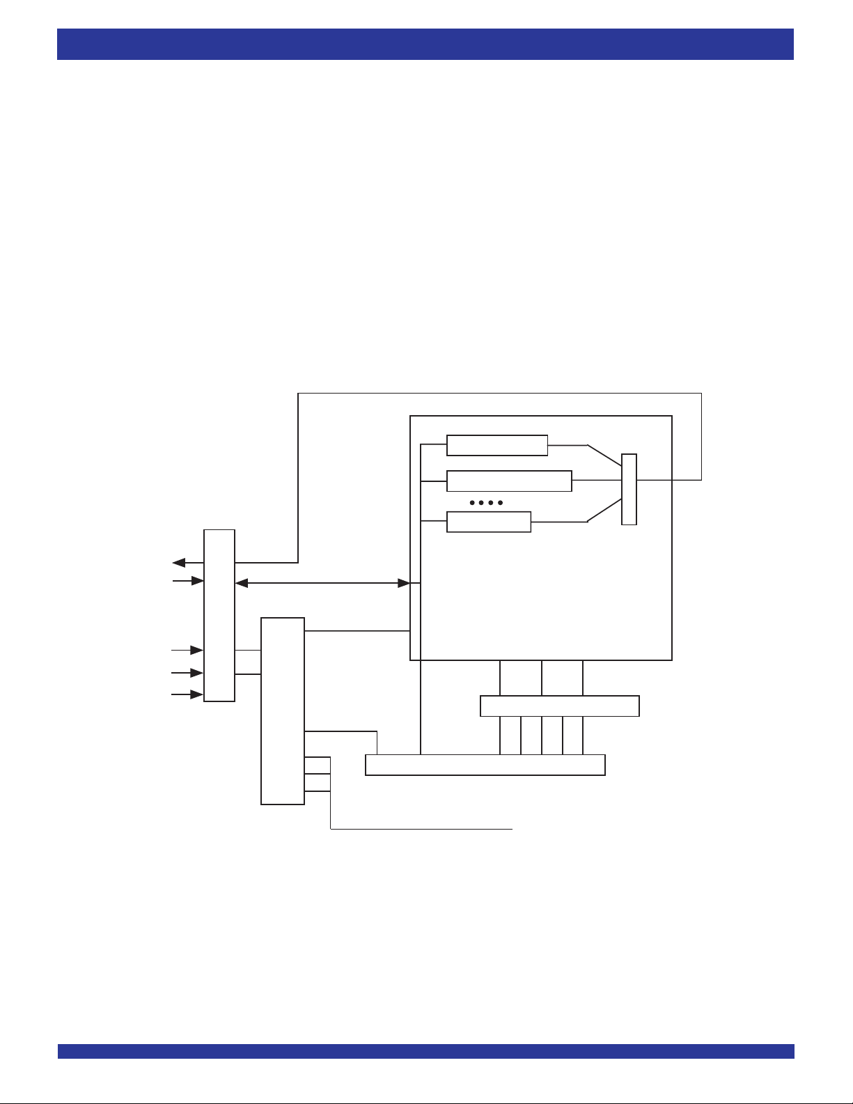
IDT72V7230/7240/7250/7260/7270/7280/7290/72100 3.3V HIGH DENSITY SUPERSYNC IITM FIFO
512 x 72, 1K x 72, 2K x 72, 4K x 72, 8K x 36, 16K x 72, 32K x 72, 64K x 72
COMMERCIAL TEMPERATURE RANGE
JTAG INTERFACE
Five additional pins (TDI, TDO, TMS, TCK and TRST) are provided to
support the JTAG boundary scan interface. The IDT72V7230/72V7240/
72V7250/72V7260/72V7270/72V7280/72V7290/72V72100 incorporates
the necessary tap controller and modified pad cells to implement the JTAG facility.
Note that IDT provides appropriate Boundary Scan Description Language
program files for these devices.
The Standard JTAG interface consists of four basic elements:
••
•
Test Access Port (TAP)
••
••
• TAP controller
••
••
• Instruction Register (IR)
••
••
• Data Register Port (DR)
••
The following sections provide a brief description of each element. For a
complete description refer to the IEEE Standard Test Access Port Specification
(IEEE Std. 1149.1-1990).
The Figure below shows the standard Boundary-Scan Architecture
DeviceID Reg.
Boundary Scan Reg.
Mux
TDO
TDI
TMS
TCLK
TRST
T
A
P
TAP
Controller
Bypass Reg.
clkDR, ShiftDR
UpdateDR
clklR, ShiftlR
UpdatelR
Instruction Register
Control Signals
Figure 6. Boundary Scan Architecture
Instruction Decode
4680 drw11
TEST ACCESS PORT (TAP)
The Tap interface is a general-purpose port that provides access to the
internal of the processor. It consists of four input ports (TCLK, TMS, TDI, TRST)
and one output port (TDO).
THE TAP CONTROLLER
The Tap controller is a synchronous finite state machine that responds to
TMS and TCLK signals to generate clock and control signals to the Instruction
and Data Registers for capture and update of data.
23
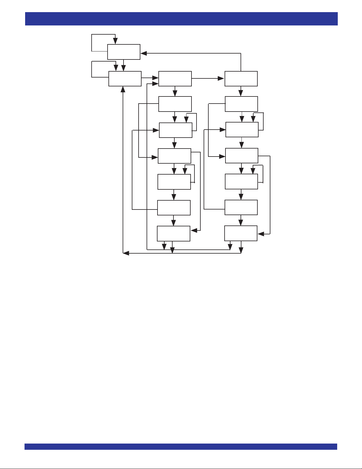
IDT72V7230/7240/7250/7260/7270/7280/7290/72100 3.3V HIGH DENSITY SUPERSYNC IITM FIFO
512 x 72, 1K x 72, 2K x 72, 4K x 72, 8K x 36, 16K x 72, 32K x 72, 64K x 72
1
Test-Logic
Reset
COMMERCIAL TEMPERATURE RANGE
0
Run-Test/
Idle
Input = TMS
0
1
Select-
1
DR-Scan
0
1
Capture-DR
0
0
1
Shift-DR
1
1
EXit1-DR
0
0
Pause-DR
1
0
Exit2-DR
0
1
Update-DR
1
SelectIR-Scan
0
Capture-IR
0
Shift-IR
1
Exit1-IR
0
Pause-IR
1
Exit2-IR
1
Update-IR
0
1
0
01
NOTES:
1. Five consecutive TCK cycles with TMS = 1 will reset the TAP.
2. TAP controller does not automatically reset upon power-up. The user must provide a reset to the TAP controller (either by TRST or TMS).
3. TAP controller must be reset before normal FIFO operations can begin.
1
0
4680 drw12
Figure 7. TAP Controller State Diagram
Refer to the IEEE Standard Test Access Port Specification (IEEE Std.
1149.1) for the full state diagram
All state transitions within the TAP controller occur at the rising edge of the
UPDATE-DR
The shifting process has been completed. The data is latched into their
parallel outputs in this state to be accessed through the internal bus.
TCLK pulse. The TMS signal level (0 or 1) determines the state progression
that occurs on each TCLK rising edge. The TAP controller takes precedence
over the FIFO memory and must be reset after power up of the device. See
TRST description for more details on TAP controller reset.
EXIT1-DR / EXIT2-DR
This is a temporary controller state. If TMS is held high, a rising edge applied
to TCK while in this state causes the controller to enter the Update-DR state. This
terminates the scanning process. All test data registers selected by the current
CAPTURE-DR
instruction retain their previous state unchanged.
Data is loaded from the parallel input pins or core outputs into the Data
Register.
PAUSE-DR
This controller state allows shifting of the test data register in the serial path
SHIFT-DR
The previously captured data is shifted in serially, LSB first at the rising edge
between TDI and TDO to be temporarily halted. All test data registers selected
by the current instruction retain their previous state unchanged.
of TCLK in the TDI/TDO path and shifted out serially, LSB first at the falling edge
of TCLK towards the output.
Capture-IR, Shift-IR and Update-IR, Exit-IR and Pause-IR are
similar to Data registers. These instructions operate on the instruction registers.
24

IDT72V7230/7240/7250/7260/7270/7280/7290/72100 3.3V HIGH DENSITY SUPERSYNC IITM FIFO
512 x 72, 1K x 72, 2K x 72, 4K x 72, 8K x 36, 16K x 72, 32K x 72, 64K x 72
COMMERCIAL TEMPERATURE RANGE
THE INSTRUCTION REGISTER
The Instruction register allows an instruction to be shifted in serially into the
processor at the rising edge of TCLK.
The Instruction is used to select the test to be performed, or the test data
register to be accessed, or both. The instruction shifted into the register is latched
at the completion of the shifting process when the TAP controller is at UpdateIR state.
The instruction register must contain 4 bit instruction register-based cells
which can hold instruction data. These mandatory cells are located nearest the
serial outputs they are the least significant bits.
TEST DATA REGISTER
The Test Data register contains three test data registers: the Bypass, the
Boundary Scan register and Device ID register.
These registers are connected in parallel between a common serial input
and a common serial data output.
The following sections provide a brief description of each element. For a
complete description, refer to the IEEE Standard Test Access Port Specification
(IEEE Std. 1149.1-1990).
TEST BYPASS REGISTER
The register is used to allow test data to flow through the device from TDI
to TDO. It contains a single stage shift register for a minimum length in serial path.
When the bypass register is selected by an instruction, the shift register stage
is set to a logic zero on the rising edge of TCLK when the TAP controller is in
the Capture-DR state.
The operation of the bypass register should not have any effect on the
operation of the device in response to the BYPASS instruction.
THE BOUNDARY-SCAN REGISTER
The Boundary Scan Register allows serial data TDI be loaded in to or read
out of the processor input/output ports. The Boundary Scan Register is a part
of the IEEE 1149.1-1990 Standard JTAG Implementation.
THE DEVICE IDENTIFICATION REGISTER
The Device Identification Register is a Read Only 32-bit register used to
specify the manufacturer, part number and version of the processor to be
determined through the TAP in response to the IDCODE instruction.
IDT JEDEC ID number is 0xB3. This translates to 0x33 when the parity
is dropped in the 11-bit Manufacturer ID field.
For the IDT72V7230/72V7240/72V7250/72V7260/72V7270/72V7280/
72V7290/72V72100, the Part Number field contains the following values:
Device Part# Field
IDT72V7230 0x57
IDT72V7240 0x51
IDT72V7250 0x52
IDT72V7260 0x53
IDT72V7270 0x54
IDT72V7280 0x55
IDT72V7290 0x56
IDT72V72100 0x50
31(MSB) 28 27 12 11 1 0(LSB)
Version (4 bits) Part Number (16-bit) Manufacturer ID (1 1-bit)
0X0 0X33 1
IDT72V7230/40/50/60/70/80/90/100
JTAG DEVICE IDENTIFICATION REGISTER
JTAG INSTRUCTION REGISTER
The Instruction register allows instruction to be serially input into the device
when the TAP controller is in the Shift-IR state. The instruction is decoded to
perform the following:
••
•
Select test data registers that may operate while the instruction is
••
current. The other test data registers should not interfere with chip
operation and the selected data register.
••
• Define the serial test data register path that is used to shift data between
••
TDI and TDO during data register scanning.
The Instruction Register is a 4 bit field (i.e.IR3, IR2, IR1, IR0) to decode 16
different possible instructions. Instructions are decoded as follows.
Hex Instruction Function
Value
0x00 EXTEST Select Boundary Scan Register
0x02 IDCODE Select Chip Identification data register
0x01 SAMPLE/PRELOAD Select Boundary Scan Register
0x03 HI-Z JTAG
0x0F BYPASS Select Bypass Register
JTAG INSTRUCTION REGISTER DECODING
The following sections provide a brief description of each instruction. For
a complete description refer to the IEEE Standard Test Access Port Specification
(IEEE Std. 1149.1-1990).
EXTEST
The mandatory EXTEST instruction is provided for external circuity and
board level interconnection check.
IDCODE
This instruction is provided to select Device Identification Register to read
out manufacture’s identity, part number and version number.
SAMPLE/PRELOAD
The mandatory SAMPLE/PRELOAD instruction allows data values to be
loaded onto the latched parallel outputs of the boundary-scan shift register prior
to selection of the boundary-scan test instruction. The SAMPLE instruction
allows a snapshot of data flowing from the system pins to the on-chip logic or
vice versa.
HIGH Z
This instruction places all the output pins on the device into a high impedance
state.
BYPASS
The Bypass instruction contains a single shift-register stage and is set to
provide a minimum-length serial path between the TDI and the TDO pins of the
device when no test operation of the device is required.
25

IDT72V7230/7240/7250/7260/7270/7280/7290/72100 3.3V HIGH DENSITY SUPERSYNC IITM FIFO
512 x 72, 1K x 72, 2K x 72, 4K x 72, 8K x 36, 16K x 72, 32K x 72, 64K x 72
t
RS
MRS
t
t
RSS
RSR
REN
t
t
RSS
RSR
WEN
t
RSS
t
FWFT/SI
t
RSS
t
RSR
LD
t
RSS
FSEL0,
FSEL1
t
RSS
BM,
OW, IW
t
RSS
BE
COMMERCIAL TEMPERATURE RANGE
RSR
RM
PFM
IP
RT
SEN
EF/OR
FF/IR
PAE
PAF, HF
t
t
t
t
RSS
t
RSS
RSS
RSS
RSS
t
t
t
RSF
t
RSF
RSF
RSF
If FWFT = HIGH, OR = HIGH
If FWFT = LOW, EF = LOW
If FWFT = LOW, FF = HIGH
If FWFT = HIGH, IR = LOW
t
RSF
(1)
Q
0
- Q
n
NOTE:
1. During Master Reset the High-Impedance control of the Qn data outputs is provided by OE only, RCS can be HIGH or LOW until the first rising edge of RCLK after Master Reset
is complete.
OE = HIGH
OE = LOW
4680 drw13
Figure 8. Master Reset Timing
26

IDT72V7230/7240/7250/7260/7270/7280/7290/72100 3.3V HIGH DENSITY SUPERSYNC IITM FIFO
512 x 72, 1K x 72, 2K x 72, 4K x 72, 8K x 36, 16K x 72, 32K x 72, 64K x 72
t
RS
PRS
t
RSS
REN
t
RSS
WEN
t
RSS
RT
t
RSS
SEN
COMMERCIAL TEMPERATURE RANGE
t
RSR
t
RSR
If FWFT = HIGH, OR = HIGH
If FWFT = LOW, EF = LOW
If FWFT = LOW, FF = HIGH
If FWFT = HIGH, IR = LOW
EF/OR
FF/IR
t
RSF
t
RSF
t
RSF
PAE
t
RSF
PAF, HF
t
RSF
(1)
0
- Q
Q
NOTE:
1. During Partial Reset the High-Impedance control of the Qn data outputs is provided by OE only, RCS can be HIGH or LOW until the first rising edge of RCLK after Partial Reset
is complete.
n
OE = HIGH
OE = LOW
4680 drw 14
Figure 9. Partial Reset Timing
27

IDT72V7230/7240/7250/7260/7270/7280/7290/72100 3.3V HIGH DENSITY SUPERSYNC IITM FIFO
512 x 72, 1K x 72, 2K x 72, 4K x 72, 8K x 36, 16K x 72, 32K x 72, 64K x 72
t
CLK
t
CLKL
(1)
t
t
DH
D
X
t
WFF
SKEW1
WCLK
D0 - D
t
t
WFF
CLKH
t
DS
NO WRITE
(1)
t
SKEW1
n
1
2
FF
WEN
RCLK
t
t
ENS
t
ENH
ENS
REN
t
RCSS
RCS
t
A
Q0 - Q
n
t
RCSLZ
DATA READ
COMMERCIAL TEMPERATURE RANGE
NO WRITE
t
ENH
1
t
A
2
t
DS
t
WFF
NEXT DATA READ
t
DH
D
X+1
t
WFF
4680 drw15
NOTES:
1. t
SKEW1 is the minimum time between a rising RCLK edge and a rising WCLK edge to guarantee that FF will go HIGH (after one WCLK cycle pus tWFF). If the time between the
rising edge of the RCLK and the rising edge of the WCLK is less than t
SKEW1, then the FF deassertion may be delayed one extra WCLK cycle.
2. LD = HIGH, OE = LOW, EF = HIGH
Figure 10. Write Cycle and Full Flag Timing (IDT Standard Mode)
t
CLKH
REF
t
CLK
t
CLKL
t
t
t
t
ENS
LAST WORD
t
OLZ
ENH
t
A
ENS
D
ENH
t
REF
t
A
0
4680 drw16
RCLK
REN
EF
Q0 - Qn
OE
WCLK
WEN
D0 - Dn
t
ENS
t
t
t
2
ENH
DH
1
t
ENH
OHZ
t
t
DS
ENS
NO OPERATION
D
1
NO OPERATION
t
REF
t
A
LAST WORD
t
OLZ
t
OE
(1)
t
SKEW1
t
t
ENS
ENH
t
DH
t
DS
D
0
t
D
1
NOTES:
SKEW1 is the minimum time between a rising WCLK edge and a rising RCLK edge to guarantee that EF will go HIGH (after one RCLK cycle plus tREF). If the time between the
1. t
rising edge of WCLK and the rising edge of RCLK is less than t
SKEW1, then EF deassertion may be delayed one extra RCLK cycle.
2. LD = HIGH.
3. First data word latency = t
SKEW1 + 1*TRCLK + tREF.
4. RCS is LOW.
Figure 11. Read Cycle, Output Enable, Empty Flag and First Data Word Latency Timing (IDT Standard Mode)
28

IDT72V7230/7240/7250/7260/7270/7280/7290/72100 3.3V HIGH DENSITY SUPERSYNC IITM FIFO
512 x 72, 1K x 72, 2K x 72, 4K x 72, 8K x 36, 16K x 72, 32K x 72, 64K x 72
COMMERCIAL TEMPERATURE RANGE
2
RCLK
1
tENS
REN
tRCSS
tRCSH
tRCSS
tRCSS
RCS
EF
Q0 - Qn
tRCSLZ
tREF
t
tA
LAST DATA-1
RCSHZ
tRCSLZ
tA
LAST DATA
t
SKEW1
tRCSHZ
(1)
tREF
WCLK
tENHtENS
WEN
tDS
Dn
tDH
Dx
NOTES:
SKEW1 is the minimum time between a rising WCLK edge and a rising RCLK edge to guarantee that EF will go HIGH (after one RCLK cycle plus tREF). If the time between the
1. t
rising edge of WCLK and the rising edge of RCLK is less than t
SKEW1, then EF deassertion may be delayed one extra RCLK cycle.
2. LD = HIGH.
3. First data word latency = t
SKEW1 + 1*TRCLK + tREF.
4. OE is LOW.
4680 drw 17
Figure 12. Read Cycle and Read Chip Select Timing (IDT Standard Mode)
29

IDT72V7230/7240/7250/7260/7270/7280/7290/72100 3.3V HIGH DENSITY SUPERSYNC IITM FIFO
512 x 72, 1K x 72, 2K x 72, 4K x 72, 8K x 36, 16K x 72, 32K x 72, 64K x 72
ENH
t
4680 drw 18
WFF
t
D
W
[D-1]
W
[D-m+2]
W
PAFS
[D-m+1]
1
W
[D-m]
W
[D-m-1]
W
DS
t
[D-m-2]
W
1
W
t
][
D-1
W
][
D-1
W
DS
t
][
D-1
W
HF
t
COMMERCIAL TEMPERATURE RANGE
ENS
t
WCLK
DS
t
DH
t
DS
t
WEN
[n+4]
W
[n+3]
W
[n +2]
W
4
W
3
W
2
W
1
W
n
- D
0
D
(2)
SKEW2
t
(1)
SKEW1
t
2
1
3
2
1
RCSS
t
RCLK
RCS
A
t
RCSLZ
t
REN
PAES
t
REF
t
PREVIOUS DATA IN OUTPUT REGISTER
n
- Q
0
Q
OR
PAE
HF
PAF
IR
Figure 13. Write Timing (First Word Fall Through Mode)
SKEW1 + 2*TRCLK + tREF.
SKEW1, then OR assertion may be delayed one extra RCLK cycle.
SKEW2, then the PAE deassertion may be delayed one extra RCLK cycle.
SKEW1 is the minimum time between a rising WCLK edge and a rising RCLK edge to guarantee that OR will go LOW after two RCLK cycles plus tREF. If the time between the rising edge of WCLK and the rising edge of RCLK
SKEW2 is the minimum time between a rising WCLK edge and a rising RCLK edge to guarantee that PAE will go HIGH after one RCLK cycle plus tPAES. If the time between the rising edge of WCLK and the rising edge of RCLK
is less than t
is less than t
3. LD = HIGH, OE = LOW
4. n = PAE offset, m = PAF offset and D = maximum FIFO depth.
5. D = 513 for IDT72V7230, 1,025 for IDT72V7240, 2,049 for IDT72V7250, 4,097 for IDT72V7260, 8,193 for IDT72V7270, 16,385 for the IDT72V7280, 32,769 for the IDT72V7290 and 65,537 for the IDT72V72100.
NOTES:
1. t
2. t
6. First data word latency = t
30

IDT72V7230/7240/7250/7260/7270/7280/7290/72100 3.3V HIGH DENSITY SUPERSYNC IITM FIFO
512 x 72, 1K x 72, 2K x 72, 4K x 72, 8K x 36, 16K x 72, 32K x 72, 64K x 72
COMMERCIAL TEMPERATURE RANGE
4680 drw 19
ENS
t
REF
t
D
W
A
t
[D-1]
W
[D-n+2]
W
[D-n+1]
W
PAES
t
1
[D-n]
W
A
t
[D-n-1]
W
][
D-1
A
W
t
][
D-1
W
HF
t
(2)
SKEW2
t
(1)
SKEW1
t
12
ENH
DH
t
t
D
W
DS
t
ENS
t
n
- D
WEN
WCLK
0
D
ENS
t
RCLK
REN
OE
A
t
OE
t
OHZ
t
PAFS
[m+4]
W
[m+3]
W
A
t
t
Figure 14. Read Timing (First Word Fall Through Mode)
m+2
W
WFF
PAF
t
WFF
t
IR
SKEW2, then the PAF deassertion may be delayed one extra WCLK cycle.
SKEW1, then the IR assertion may be delayed one extra WCLK cycle.
SKEW1 is the minimum time between a rising RCLK edge and a rising WCLK edge to guarantee that IR will go LOW after one WCLK cycle plus tWFF. If the time between the rising edge of RCLK and the rising edge of WCLK
SKEW2 is the minimum time between a rising RCLK edge and a rising WCLK edge to guarantee that PAF will go HIGH after one WCLK cycle plus tPAFS. If the time between the rising edge of RCLK and the rising edge of WCLK
is less than t
is less than t
NOTES:
1. t
2. t
3. LD = HIGH.
4. n = PAE Offset, m = PAF offset and D = maximum FIFO depth.
5. D = 513 for IDT72V7230, 1,025 for IDT72V7240, 2,049 for IDT72V7250, 4,097 for IDT72V7260, 8,193 for IDT72V7270, 16,385 for the IDT72V7280, 32,769 for the IDT72V7290 and 65,537 for the IDT72V72100.
6. RCS = LOW.
3
W
A
t
2
W
1
W
1
W
n
- Q
0
Q
OR
PAE
HF
31

IDT72V7230/7240/7250/7260/7270/7280/7290/72100 3.3V HIGH DENSITY SUPERSYNC IITM FIFO
512 x 72, 1K x 72, 2K x 72, 4K x 72, 8K x 36, 16K x 72, 32K x 72, 64K x 72
COMMERCIAL TEMPERATURE RANGE
4680 drw 20
ENS
t
REF
t
D
W
A
t
[D-1]
W
[D-n+2]
W
[D-n+1]
W
PAES
t
1
[D-n]
W
A
t
[D-n-1]
W
][
D-1
A
W
t
][
D-1
W
HF
t
(2)
SKEW2
t
(1)
SKEW1
t
12
ENH
DH
t
t
D
W
DS
t
ENS
t
n
- D
WEN
WCLK
0
D
ENS
t
RCLK
RCSH
t
RCSS
t
REN
RCSHZ
t
RCS
A
t
A
t
RCSLZ
t
[m+4]
W
[m+3]
W
m+2
W
3
W
2
W
1
W
n
- Q
0
Q
OR
PAE
HF
PAFS
t
PAF
WFF
t
WFF
t
IR
Figure 15. Read Cycle and Read Chip Select Timing (First Word Fall Through Mode)
SKEW2, then the PAF deassertion may be delayed one extra WCLK cycle.
SKEW1, then the IR assertion may be delayed one extra WCLK cycle.
SKEW1 is the minimum time between a rising RCLK edge and a rising WCLK edge to guarantee that IR will go LOW after one WCLK cycle plus tWFF. If the time between the rising edge of RCLK and the rising edge of WCLK
SKEW2 is the minimum time between a rising RCLK edge and a rising WCLK edge to guarantee that PAF will go HIGH after one WCLK cycle plus tPAFS. If the time between the rising edge of RCLK and the rising edge of WCLK
is less than t
is less than t
NOTES:
1. t
2. t
3. LD = HIGH.
4. n = PAE Offset, m = PAF offset and D = maximum FIFO depth.
5. D = 513 for IDT72V7230, 1,025 for IDT72V7240, 2,049 for IDT72V7250, 4,097 for IDT72V7260, 8,193 for IDT72V7270, 16,385 for the IDT72V7280, 32,769 for the IDT72V7290 and 65,537 for the IDT72V72100.
6. OE = LOW.
32

IDT72V7230/7240/7250/7260/7270/7280/7290/72100 3.3V HIGH DENSITY SUPERSYNC IITM FIFO
512 x 72, 1K x 72, 2K x 72, 4K x 72, 8K x 36, 16K x 72, 32K x 72, 64K x 72
COMMERCIAL TEMPERATURE RANGE
RCLK
REN
Q
- Q
0
WCLK
WEN
PAE
RT
EF
1
t
t
t
A
ENH
t
RTS
t
SKEW2
W
x+1
t
ENS
n
W
x
ENS
2
t
ENH
t
t
A
(3)
W
1
A
(3)
W
2
12
t
RTS
t
t
ENS
ENH
t
REF
t
HF
t
REF
t
PAES
HF
t
PAFS
PAF
4680 drw21
NOTES:
1. Retransmit setup is complete after EF returns HIGH, only then can a read operation begin.
2. OE = LOW; RCS = LOW.
1 = first word written to the FIFO after Master Reset, W2 = second word written to the FIFO after Master Reset.
3. W
4. No more than D - 2 may be written to the FIFO between Reset (Master or Partial) and Retransmit setup. Therefore, FF will be HIGH throughout the Retransmit setup procedure.
D = 512 for IDT72V7230, 1,024 for IDT72V7240, 2,048 for IDT72V7250, 4,096 for IDT72V7260, 8,192 for IDT72V7270, 16,384 for the IDT72V7280, 32,768 for the IDT72V7290
and 65,536 for the IDT72V72100.
5. There must be at least two words written to the FIFO before a Retransmit operation can be invoked.
6. RM is set HIGH during MRS.
Figure 16. Retransmit Timing (IDT Standard Mode)
33

IDT72V7230/7240/7250/7260/7270/7280/7290/72100 3.3V HIGH DENSITY SUPERSYNC IITM FIFO
512 x 72, 1K x 72, 2K x 72, 4K x 72, 8K x 36, 16K x 72, 32K x 72, 64K x 72
COMMERCIAL TEMPERATURE RANGE
RCLK
tENS
tENH
tRTS
1
tENS
2
3
4
tENH
REN
0
- Q
Q
WCLK
tA
n
W
x
tRTS
W
x+1
tSKEW2
12
W
(4)
1
W
tAtA
(4)
2
W
3
tA
(4)
W
4
WEN
tENS
RT
tENH
tREF
tREF
OR
tPAES
PAE
tHF
HF
tPAFS
PAF
4680 drw22
NOTES:
1. Retransmit setup is complete after OR returns LOW.
2. No more than D - 2 words may be written to the FIFO between Reset (Master or Partial) and Retransmit setup. Therefore, IR will be LOW throughout the Retransmit setup procedure.
D = 513 for the IDT72V7230, 1,025 for the IDT72V7240, 2,049 for the IDT72V7250, 4,097 for the IDT72V7260, 8,193 for the IDT72V7270, 16,385 for the IDT72V7280, 32,769 for
the IDT72V7290 and 65,537 for the IDT72V72100.
3. OE = LOW; RCS = LOW.
1, W2, W3 = first, second and third words written to the FIFO after Master Reset.
4. W
5. There must be at least two words written to the FIFO before a Retransmit operation can be invoked.
6. RM is set HIGH during MRS.
Figure 17. Retransmit Timing (FWFT Mode)
34

IDT72V7230/7240/7250/7260/7270/7280/7290/72100 3.3V HIGH DENSITY SUPERSYNC IITM FIFO
512 x 72, 1K x 72, 2K x 72, 4K x 72, 8K x 36, 16K x 72, 32K x 72, 64K x 72
COMMERCIAL TEMPERATURE RANGE
RCLK
REN
0
- Q
Q
WCLK
WEN
PAE
PAF
RT
EF
HF
1
t
ENS
t
A
n
W
x
W
x+1
A
t
t
SKEW2
W
0
2
t
A
(3)
W
1
3
t
ENH
t
t
A
(3)
(3)
W
2
A
W
3
12
t
RTS
t
t
ENS
ENH
t
HF
t
PAFS
t
PAES
4680 drw23
NOTES:
1. If the part is empty at the point of Retransmit, the empty flag (EF) will be updated based on RCLK (Retransmit clock cycle), valid data will also appear on the output.
2. OE = LOW; RSC = LOW.
0 = first word written to the FIFO after Master Reset, W1 = second word written to the FIFO after Master Reset.
3. W
4. No more than D - 2 may be written to the FIFO between Reset (Master or Partial) and Retransmit setup. Therefore, FF will be HIGH throughout the Retransmit setup procedure.
D = 512 for IDT72V7230, 1,024 for IDT72V7240, 2,048 for IDT72V7250, 4,096 for IDT72V7260, 8,192 for IDT72V7270, 16,384 for the IDT72V7280, 32,768 for the IDT72V7290
and 65,536 for the IDT72V72100.
5. There must be at least two words written to the FIFO before a Retransmit operation can be invoked.
6. RM is set LOW during MRS.
Figure 18. Zero Latency Retransmit Timing (IDT Standard Mode)
35
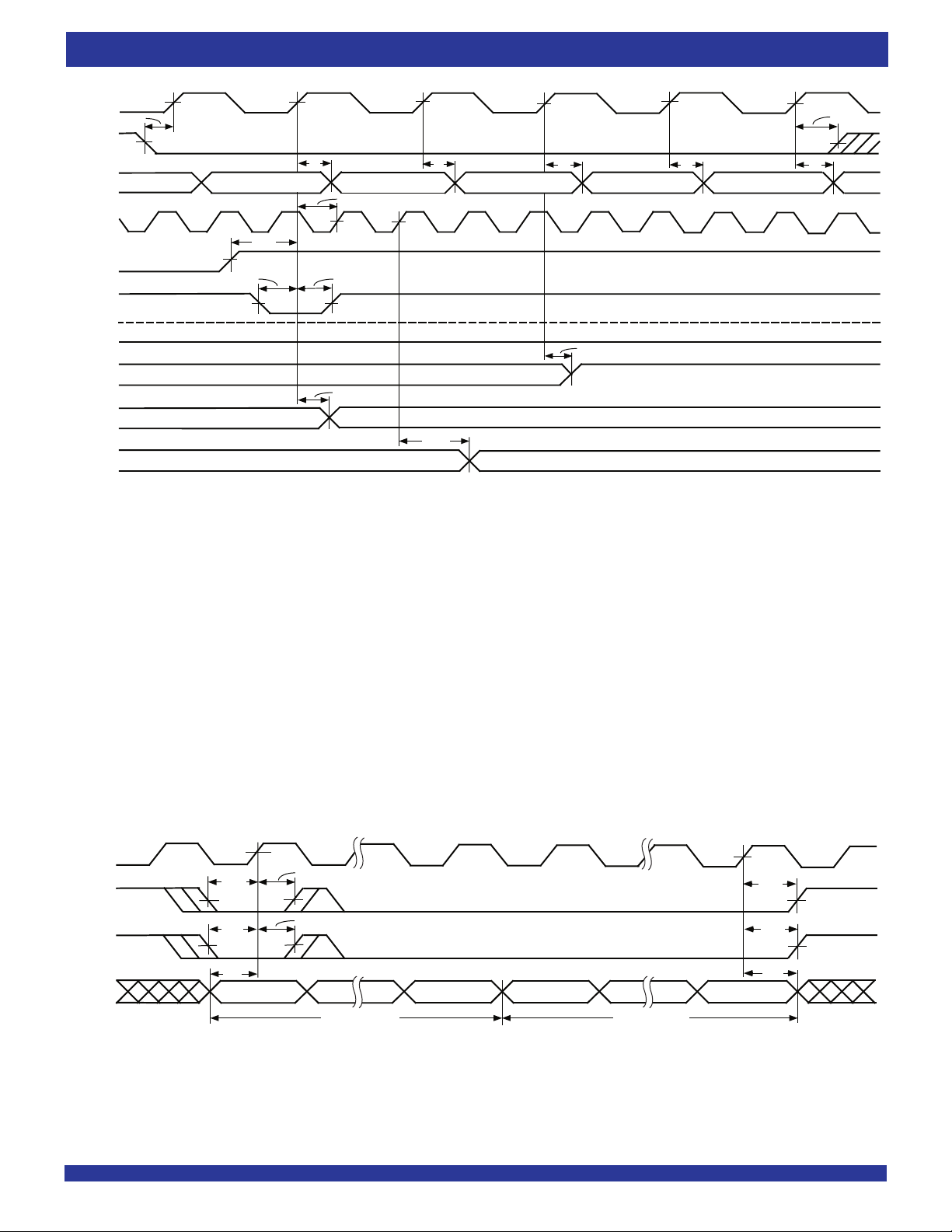
IDT72V7230/7240/7250/7260/7270/7280/7290/72100 3.3V HIGH DENSITY SUPERSYNC IITM FIFO
512 x 72, 1K x 72, 2K x 72, 4K x 72, 8K x 36, 16K x 72, 32K x 72, 64K x 72
COMMERCIAL TEMPERATURE RANGE
RCLK
t
ENS
1
2
3
4
5
t
ENH
REN
t
0
- Q
Q
WCLK
A
n
W
x
W
t
RTS
x+1
W1
t
SKEW2
12
t
A
W
t
A
(4)
2
t
A
(4)
W
3
W
t
A
(4)
4
W
5
WEN
t
ENS
t
ENH
RT
OR
t
PAES
PAE
t
HF
HF
t
PAFS
PAF
4680 drw24
NOTES:
1. If the part is empty at the point of Retransmit, the output ready flag (OR) will be updated based on RCLK (Retransmit clock cycle), valid data will also appear on the output.
2. No more than D - 2 words may be written to the FIFO between Reset (Master or Partial) and Retransmit setup. Therefore, IR will be LOW throughout the Retransmit setup procedure.
D = 513 for the IDT72V7230, 1,025 for the IDT72V7240, 2,049 for the IDT72V7250, 4,097 for the IDT72V7260, 8,193 for the IDT72V7270, 16,385 for the IDT72V7280, 32,769 for
the IDT72V7290 and 65,537 for the IDT72V72100.
3. OE = LOW; RCS = LOW.
1, W2, W3 = first, second and third words written to the FIFO after Master Reset.
4. W
5. There must be at least two words written to the FIFO before a Retransmit operation can be invoked.
6. RM is set LOW during MRS.
Figure 19. Zero Latency Retransmit Timing (FWFT Mode)
SCLK
t
t
ENS
SEN
t
LDS
LD
t
DS
SI
NOTE:
1. X = 9 for the IDT72V7230, X= 10 for the IDT72V7240, X = 11 for the IDT72V7250, X = 12 for the IDT72V7260, X = 13 for the IDT72V7270, X = 14 for the IDT72V7280,
X = 15 for the IDT72V7290 and X = 16 for the IDT72V72100.
BIT 0
ENH
t
LDH
EMPTY OFFSET
BIT X
t
ENH
t
LDH
t
(1)
BIT 0
FULL OFFSET
BIT X
DH
(1)
4680 drw25
Figure 20. Serial Loading of Programmable Flag Registers (IDT Standard and FWFT Modes)
36
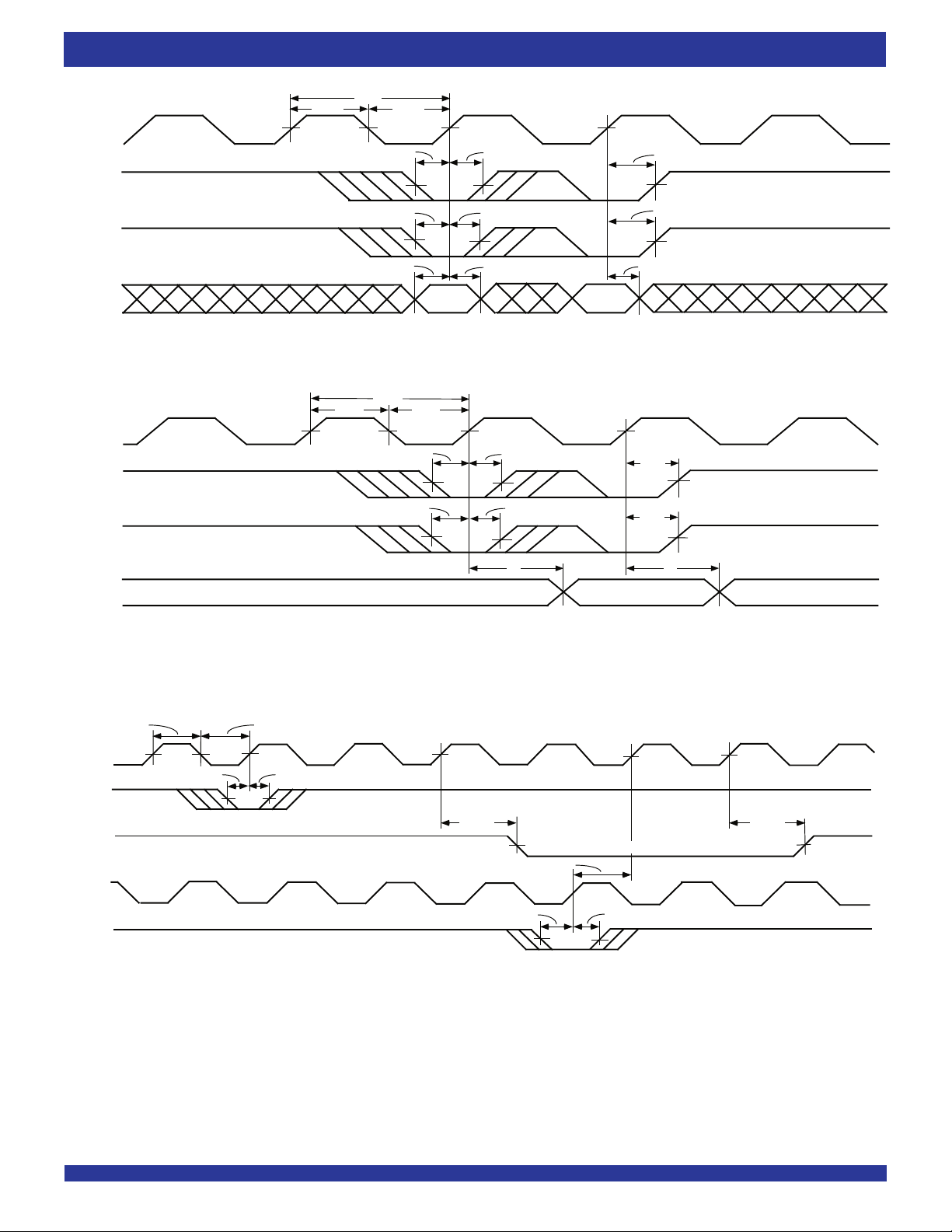
IDT72V7230/7240/7250/7260/7270/7280/7290/72100 3.3V HIGH DENSITY SUPERSYNC IITM FIFO
512 x 72, 1K x 72, 2K x 72, 4K x 72, 8K x 36, 16K x 72, 32K x 72, 64K x 72
t
CLKH
CLK
t
CLKL
t
WCLK
t
t
LDS
LDH
LD
t
t
ENS
ENH
WEN
DS
t
0
- D
n
D
PAE
OFFSET
t
DH
OFFSET
Figure 21. Parallel Loading of Programmable Flag Registers (IDT Standard and FWFT Modes)
t
CLK
t
CLKL
t
LDS
t
LDH
RCLK
LD
t
CLKH
PAF
COMMERCIAL TEMPERATURE RANGE
t
LDH
t
ENH
t
DH
4680 drw26
t
LDH
REN
0
- Q
16
Q
NOTES:
1. OE = LOW; RCS = LOW.
t
CLKL
WCLK
WEN
PAF
RCLK
REN
t
ENS
DATA IN OUTPUT REGISTER PAE OFFSET
t
ENH
t
A
t
ENH
t
A
Figure 22. Parallel Read of Programmable Flag Registers (IDT Standard and FWFT Modes)
t
CLKL
12
D - m words in FIFO
t
ENH
(2)
t
ENS
t
ENH
D - (m+1) words in FIFO
1
(2)
2
t
PAFS
(3)
t
SKEW2
t
ENS
PAF OFFSET
t
PAFS
4680 drw27
D-(m+1) words
(2)
in FIFO
4680 drw 28
NOTES:
1. m = PAF offset.
2. D = maximum FIFO depth.
In IDT Standard mode: D = 512 for the IDT72V7230, 1,024 for the IDT72V7240, 2,048 for the IDT72V7250, 4,096 for the IDT72V7260 and 8,192 for the IDT72V7270, 16,384 for
the IDT72V7280, 32,768 for the IDT72V7290 and 65,536 for the IDT72V72100.
In FWFT mode: D = 513 for the IDT72V7230, 1,025 for the IDT72V7240, 2,049 for the IDT72V7250, 4,097 for the IDT72V7260, 8,193 for the IDT72V7270, 16,385 for the IDT72V7280,
32,769 for the IDT72V7290 and 65,537 for the IDT72V72100.
t
SKEW2
is the minimum time between a rising RCLK edge and a rising WCLK edge to guarantee that PAF will go HIGH (after one WCLK cycle plus t
3.
rising edge of RCLK and the rising edge of WCLK is less than t
SKEW2
, then the PAF deassertion time may be delayed one extra WCLK cycle.
PAFS
). If the time between the
4. PAF is asserted and updated on the rising edge of WCLK only.
5. Select this mode by setting PFM HIGH during Master Reset.
Figure 23. Synchronous Programmable Almost-Full Flag Timing (IDT Standard and FWFT Modes)
37
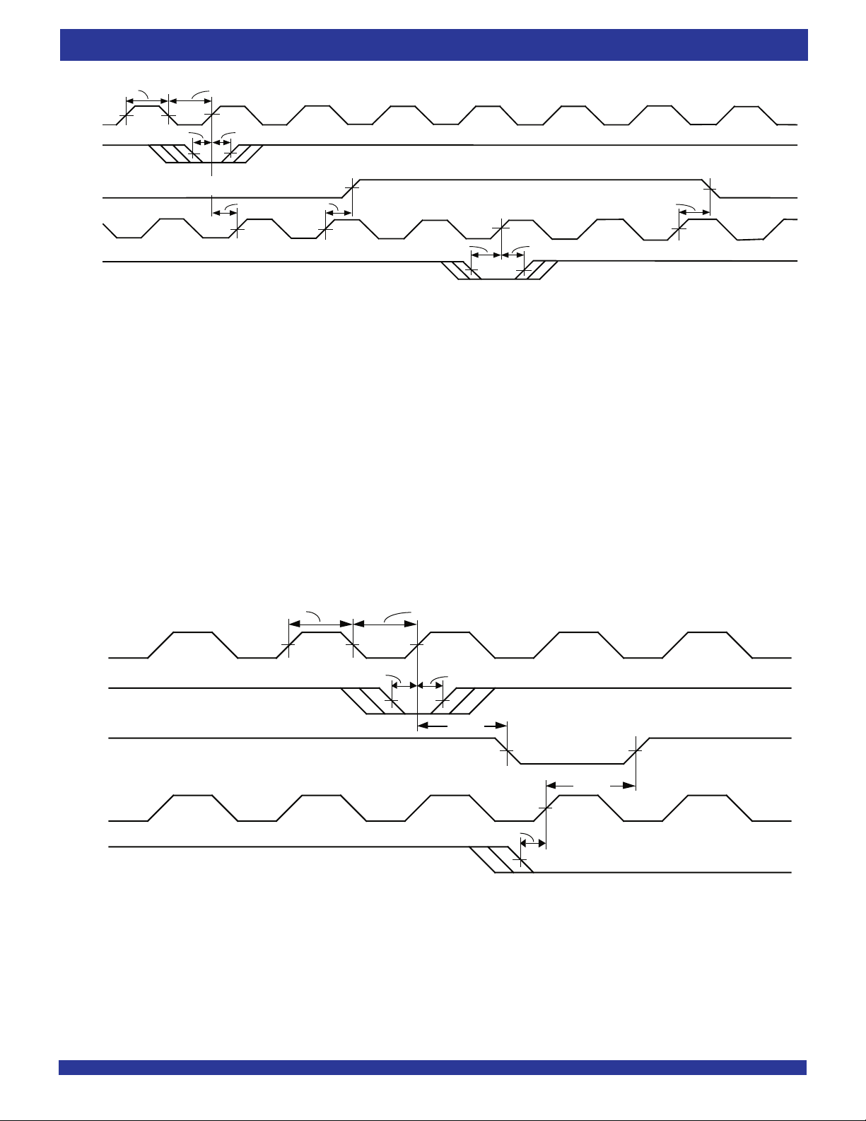
IDT72V7230/7240/7250/7260/7270/7280/7290/72100 3.3V HIGH DENSITY SUPERSYNC IITM FIFO
512 x 72, 1K x 72, 2K x 72, 4K x 72, 8K x 36, 16K x 72, 32K x 72, 64K x 72
COMMERCIAL TEMPERATURE RANGE
tCLKH
tCLKL
WCLK
tENS
tENH
WEN
(2)
PAE
RCLK
REN
n words in FIFO
n+1 words in FIFO
,
(3)
(4)
tSKEW2
12 12
tPAES
n+1 words in FIFO
n+2 words in FIFO
tENS
tENH
(2)
,
(3)
tPAES
n words in FIFO
n+1 words in FIFO
4680 drw29
NOTES:
1. n = PAE offset.
2. For IDT Standard mode
3. For FWFT mode.
tSKEW2 is the minimum time between a rising WCLK edge and a rising RCLK edge to guarantee that PAE will go HIGH (after one RCLK cycle plus tPAES). If the time between the
4.
rising edge of WCLK and the rising edge of RCLK is less than t
SKEW2, then the PAE deassertion may be delayed one extra RCLK cycle.
5. PAE is asserted and updated on the rising edge of WCLK only.
6. Select this mode by setting PFM HIGH during Master Reset.
7. RCS is LOW.
Figure 24. Synchronous Programmable Almost-Empty Flag Timing (IDT Standard and FWFT Modes)
(2)
,
(3)
t
CLKH
t
CLKL
WCLK
t
ENS
t
ENH
WEN
t
PAF
PAFA
D - (m + 1) words in FIFO
D - m words
in FIFO
t
PAFA
D - (m + 1) words
in FIFO
RCLK
t
ENS
REN
4680 drw30
NOTES:
1. m = PAF offset.
2. D = maximum FIFO Depth.
In IDT Standard Mode:
IDT72V7280, 32,768 for the IDT72V7290 and 65,536 for the IDT72V72100.
In FWFT Mode: D = 513 for the IDT72V7230, 1,025 for the IDT72V7240, 2,049 for the IDT72V7250, 4,097 for the IDT72V7260, 8,193 for the IDT72V7270, 16,385 for the IDT72V7280,
32,769 for the IDT72V7290 and 65,537 for the IDT72V72100.
3. PAF is asserted to LOW on WCLK transition and reset to HIGH on RCLK transition.
4. Select this mode by setting PFM LOW during Master Reset.
D = 512 for the IDT72V7230, 1,024 for the IDT72V7240, 2,048 for the IDT72V7250, 4,096 for the IDT72V7260, 8,192 for the IDT72V7270, 16,384 for the
Figure 25. Asynchronous Programmable Almost-Full Flag Timing (IDT Standard and FWFT Modes)
38

IDT72V7230/7240/7250/7260/7270/7280/7290/72100 3.3V HIGH DENSITY SUPERSYNC IITM FIFO
512 x 72, 1K x 72, 2K x 72, 4K x 72, 8K x 36, 16K x 72, 32K x 72, 64K x 72
t
CLKH
t
CLKL
WCLK
t
ENS
t
ENH
WEN
COMMERCIAL TEMPERATURE RANGE
(2)
,
(3)
PAE
n words in FIFO
n + 1 words in FIFO
RCLK
REN
NOTES:
1. n = PAE offset.
2. For IDT Standard Mode.
3. For FWFT Mode.
4. PAE is asserted LOW on RCLK transition and reset to HIGH on WCLK transition.
5. Select this mode by setting PFM LOW during Master Reset.
Figure 26. Asynchronous Programmable Almost-Empty Flag Timing (IDT Standard and FWFT Modes)
t
PAEA
n + 1 words in FIFO
n + 2 words in FIFO
t
ENS
t
PAEA
(2)
,
(3)
n words in FIFO
n + 1 words in FIFO
(2)
,
(3)
4680 drw 31
t
t
CLKH
CLKL
WCLK
t
t
ENS
ENH
WEN
t
HF
D/2 words in FIFO
D-1
[
+ 1] words in FIFO
2
(1)
,
(2)
HF
D/2 + 1 words in FIFO
D-1
[
+ 2] words in FIFO
2
(1)
,
(2)
t
HF
D/2 words in FIFO
D-1
[
+ 1] words in FIFO
2
(1)
,
(2)
RCLK
t
ENS
REN
4680 drw32
NOTES:
1. In IDT Standard mode: D = maximum FIFO depth. D = 512 for the IDT72V7230, 1,024 for the IDT72V7240, 2,048 for the IDT72V7250, 4,096 for the IDT72V7260, 8,192 for the
IDT72V7270, 16,384 for the IDT72V7280, 32,768 for the IDT72V7290 and 65,536 for the IDT72V72100.
2. In FWFT mode: D = maximum FIFO depth. D = 513 for the IDT72V7230, 1,025 for the IDT72V7240, 2,049 for the IDT72V7250, 4,097 for the IDT72V7260, 8,193 for the IDT72V7270,
16,385 for the IDT72V7280, 32,769 for the IDT72V7290 and 65,537 for the IDT72V72100.
Figure 27. Half-Full Flag Timing (IDT Standard and FWFT Modes)
39

IDT72V7230/7240/7250/7260/7270/7280/7290/72100 3.3V HIGH DENSITY SUPERSYNC IITM FIFO
512 x 72, 1K x 72, 2K x 72, 4K x 72, 8K x 36, 16K x 72, 32K x 72, 64K x 72
COMMERCIAL TEMPERATURE RANGE
OPTIONAL CONFIGURATIONS
WIDTH EXPANSION CONFIGURATION
Word width may be increased simply by connecting together the control
signals of multiple devices. Status flags can be detected from any one device.
The exceptions are the EF and FF functions in IDT Standard mode and the IR
and OR functions in FWFT mode. Because of variations in skew between RCLK
and WCLK, it is possible for EF/FF deassertion and IR/OR assertion to vary
by one cycle between FIFOs. In IDT Standard mode, such problems can be
PARTIAL RESET (PRS)
MASTER RESET (MRS)
FIRST WORD FALL THROUGH/
SERIAL INPUT (FWFT/SI)
GATE
(1)
RETRANSMIT (RT)
DATA IN
m + n m n
WRITE CLOCK (WCLK)
WRITE ENABLE (WEN)
FULL FLAG/INPUT READY (FF/IR)
FULL FLAG/INPUT READY (FF/IR) #2
PROGRAMMABLE (PAF)
HALF-FULL FLAG (HF)
D0 - Dm
LOAD (LD)
72V7230
72V7240
72V7250
72V7260
72V7270
#1
72V7280
72V7290
72V72100
FIFO
IDT
#1
Dm+1 - Dn
m
avoided by creating composite flags, that is, ANDing EF of every FIFO, and
separately ANDing FF of every FIFO. In FWFT mode, composite flags can be
created by ORing OR of every FIFO, and separately ORing IR of every FIFO.
Figure 28 demonstrates a width expansion using two IDT72V7230/
72V7240/72V7250/72V7260/72V7270/72V7280/72V7290/72V72100 devices. D
0 - D71 from each device form a 144-bit wide input bus and Q0-Q71
from each device form a 144-bit wide output bus. Any word width can be attained
by adding additional IDT72V7230/72V7240/72V7250/72V7260/72V7270/
72V7280/72V7290/72V72100 devices.
READ CLOCK (RCLK)
READ SHIP SELECT (RCS)
IDT
72V7230
72V7240
72V7250
72V7260
72V7270
72V7280
72V7290
72V72100
FIFO
#2
READ ENABLE (REN)
OUTPUT ENABLE (OE)
PROGRAMMABLE (PAE)
EMPTY FLAG/OUTPUT READY (EF/OR) #1
EMPTY FLAG/OUTPUT READY (EF/OR) #2
n
Qm+1 - Qn
m + n
DATA OUT
GATE
(1)
Q
0
-
Q
m
4680 drw 33
NOTES:
1. Use an AND gate in IDT Standard mode, an OR gate in FWFT mode.
2. Do not connect any output control signals directly together.
3. FIFO #1 and FIFO #2 must be the same depth, but may be different word widths.
Figure 28. Block Diagram of 512 x 144, 1,024 x 144, 2,048 x 144, 4,096 x 144, 8,192 x 144, 16,384 x 144, 32,768 x 144 and 65,536 x 144 Width Expansion
40

IDT72V7230/7240/7250/7260/7270/7280/7290/72100 3.3V HIGH DENSITY SUPERSYNC IITM FIFO
512 x 72, 1K x 72, 2K x 72, 4K x 72, 8K x 36, 16K x 72, 32K x 72, 64K x 72
FWFT/SI
TRANSFER CLOCK
WRITE CLOCK
WRITE ENABLE
INPUT READY
DATA IN
n n
WCLK
WEN
IR
Dn
FWFT/SI FWFT/SI
IDT
72V7230
72V7240
72V7250
72V7260
72V7270
72V7280
72V7290
72V72100
RCLK
OR
REN
RCS
OE
Qn
GND
n
WCLK
WEN
IR
Dn
COMMERCIAL TEMPERATURE RANGE
READ CLOCK
READ CIP SELECT
READ ENABLE
OUTPUT READY
OUTPUT ENABLE
DATA OUT
4680 drw34
IDT
72V7230
72V7240
72V7250
72V7260
72V7270
72V7280
72V7290
72V72100
RCLK
RCS
REN
OR
OE
Qn
Figure 29. Block Diagram of 1,024 x 72, 2,048 x 72, 4,096 x 72, 8,192 x 72, 16,384 x 72, 32,768 x 72, 65,572 x 72 and 131,072 x 72 Depth Expansion
DEPTH EXPANSION CONFIGURATION (FWFT MODE ONLY)
The IDT72V7230 can easily be adapted to applications requiring depths
greater than 512, 1,024 for the IDT72V7240, , 2,048 for the IDT72V7250,
4,096 for the IDT72V7260, 8,192 for the IDT72V7270, 16,384 for the
IDT72V7280, 32,768 for the IDT72V7290 and 65,536 for the IDT72V72100
with an 72-bit bus width. In FWFT mode, the FIFOs can be connected in series
(the data outputs of one FIFO connected to the data inputs of the next) with no
external logic necessary. The resulting configuration provides a total depth
equivalent to the sum of the depths associated with each single FIFO. Figure
29 shows a depth expansion using two IDT72V7230/72V7240/72V7250/
72V7260/72V7270/72V7280/72V7290/72V72100 devices.
Care should be taken to select FWFT mode during Master Reset for all FIFOs
in the depth expansion configuration. The first word written to an empty
configuration will pass from one FIFO to the next ("ripple down") until it finally
appears at the outputs of the last FIFO in the chain – no read operation is
necessary but the RCLK of each FIFO must be free-running. Each time the
data word appears at the outputs of one FIFO, that device's OR line goes LOW,
enabling a write to the next FIFO in line.
For an empty expansion configuration, the amount of time it takes for OR of
the last FIFO in the chain to go LOW (i.e. valid data to appear on the last FIFO's
outputs) after a word has been written to the first FIFO is the sum of the delays
for each individual FIFO:
(N – 1)*(4*transfer clock) + 3*T
RCLK
where N is the number of FIFOs in the expansion and TRCLK is the RCLK
period. Note that extra cycles should be added for the possibility that the tSKEW1
specification is not met between WCLK and transfer clock, or RCLK and transfer
clock, for the OR flag.
The "ripple down" delay is only noticeable for the first word written to an empty
depth expansion configuration. There will be no delay evident for subsequent
words written to the configuration.
The first free location created by reading from a full depth expansion
configuration will "bubble up" from the last FIFO to the previous one until it finally
moves into the first FIFO of the chain. Each time a free location is created in one
FIFO of the chain, that FIFO's IR line goes LOW, enabling the preceding FIFO
to write a word to fill it.
For a full expansion configuration, the amount of time it takes for IR of the first
FIFO in the chain to go LOW after a word has been read from the last FIFO is
the sum of the delays for each individual FIFO:
(N – 1)*(3*transfer clock) + 2 TWCLK
where N is the number of FIFOs in the expansion and TWCLK is the WCLK
period. Note that extra cycles should be added for the possibility that the tSKEW1
specification is not met between RCLK and transfer clock, or WCLK and transfer
clock, for the IR flag.
The Transfer Clock line should be tied to either WCLK or RCLK, whichever
is faster. Both these actions result in data moving, as quickly as possible, to the
end of the chain and free locations to the beginning of the chain.
41

ORDERING INFORMATION
IDT XXXXX
Device TypeXPower
NOTE:
1. Industrial temperature range is available by special order.
XX
Speed
X
Package
X
Process /
Temperature
Range
BLANK
BB
10
15
L
72V7230
72V7240
72V7250
72V7260
72V7270
72V7280
72V7290
72V72100
Commercial (0°C to +70°C)
Fine Pitch Ball Grid Array (PBGA, BB256−1)
Commercial
Low Power
512 x 72 3.3V SuperSync II FIFO
1,024 x 72 3.3V SuperSync II FIFO
2,048 x 72 3.3V SuperSync II FIFO
4,096 x 72 3.3V SuperSync II FIFO
8,192 x 72 3.3V SuperSync II FIFO
16,384 x 72 3.3V SuperSync II FIFO
32,768 x 72 3.3V SuperSync II FIFO
65,536 x 72 3.3V SuperSync II FIFO
Clock Cycle Time (t
Speed in Nanoseconds
CLK
4680 drw35
)
DATASHEET DOCUMENT HISTORY
06/01/2000 pgs. 1, 2, 3, 7, 33, 34, 34, 35, 38, 41, and 42.
11/01/2000 pgs. 1, 2, and 42.
01/10/2001 pg. 7.
04/12/2001 pgs. 3, 4, 5, 17, 26, and 27.
05/01/2001 pg. 23.
10/04/2001 pg. 36.
12/16/2002 pgs. 1, 4, 6, 22, 24, and 41.
02/11/2003 pgs. 6, and 24.
09/29/2003 pg. 7.
12/17/2003 pg. 35.
CORPORATE HEADQUARTERS for SALES: for Tech Support:
2975 Stender Way 800-345-7015 or 408-727-6116 408-330-1753
Santa Clara, CA 95054 fax: 408-492-8674 email : FI FOhelp@idt.com
www.idt.com
42

Copyright © Each Manufacturing Company.
All Datasheets cannot be modified without permission.
This datasheet has been download from :
www.AllDataSheet.com
100% Free DataSheet Search Site.
Free Download.
No Register.
Fast Search System.
www.AllDataSheet.com
 Loading...