

Page 1
CMOS SyncBiFIFO
256 x 18 x 2
512 x 18 x 2
TM
IDT72605
IDT72615
FEATURES:
••
•
Two independent FIFO memories for fully bidirectional data
••
transfers
••
256 x 18 x 2 organization (IDT72605)
•
••
••
• 512 x 18 x 2 organization (IDT72615)
••
••
• Synchronous interface for fast (20ns) read and write cycle times
••
••
• Each data port has an independent clock and read/write control
••
••
• Output enable is provided on each port as a three-state control
••
of the data bus
••
Built-in bypass path for direct data transfer between two ports
•
••
••
• Two fixed flags, Empty and Full, for both the A-to-B and the B-
••
to-A FIFO
••
• Programmable flag offset can be set to any depth in the FIFO
••
••
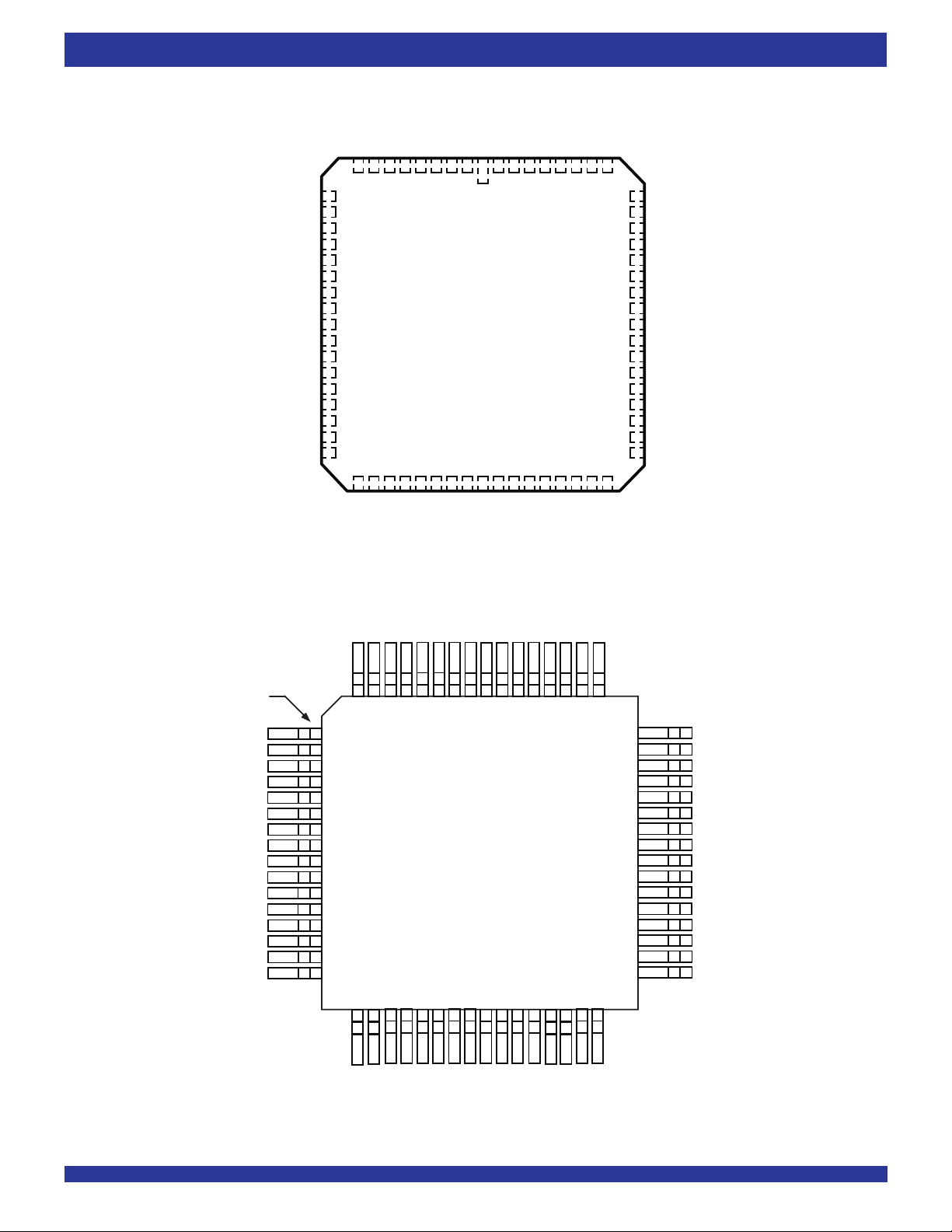
• The synchronous BiFIFO is packaged in a 64-pin TQFP (Thin
••
Quad Flatpack) and 68-pin PLCC
••
• Industrial temperature range (–40
••
°°
°C to +85
°°
°°
°C)
°°
DESCRIPTION:
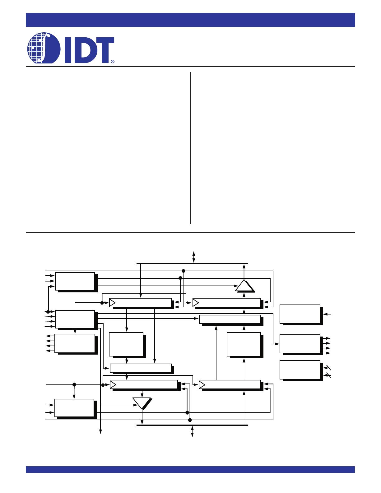
The IDT72605 and IDT72615 are very high-speed, low-power bidirec-
tional First-In, First-Out (FIFO) memories, with synchronous interface for fast
FUNCTIONAL BLOCK DIAGRAM
read and write cycle times. The SyncBiFIFO™ is a data buffer that can store
or retrieve information from two sources simultaneously. Two Dual-Port FIFO
memory arrays are contained in the SyncBiFIFO; one data buffer for each
direction.
The SyncBiFIFO has registers on all inputs and outputs. Data is only
transferred into the I/O registers on clock edges, hence the interfaces are
synchronous. Each Port has its own independent clock. Data transfers to the
I/O registers are gated by the enable signals. The transfer direction for each
port is controlled independently by a read/write signal. Individual output enable
signals control whether the SyncBiFIFO is driving the data lines of a port or
whether those data lines are in a high-impedance state.
Bypass control allows data to be directly transferred from input to output
register in either direction.
The SyncBiFIFO has eight flags. The flag pins are Full, Empty, Almost-Full,
and Almost-Empty for both FIFO memories. The offset depths of the Almost-Full
and Almost-Empty flags can be programmed to any location.
The SyncBiFIFO is fabricated using IDT’s high-speed, submicron CMOS
technology.
DA0-D
A17
EN
R/W
OE
CS
EF
PAE
PAF
FF
CLK
OE
R/W
EN
A
A
A
HIGH
Z
CONTROL
CLK
A
A
A
2
A
1
A
0
AB
AB
AB
AB
µP
INTERFACE
FLAG
LOGIC
INPUT REGISTER
MEMORY
ARRAY
512 x 18
256 x 18
MUX
B
B
B
B
HIGH
Z
CONTROL
BYP
OUTPUT REGISTER INPUT REGISTER
B
DB0-D
OUTPUT REGISTER
MUX
MEMORY
512 x 18
256 x 18
B17
ARRAY
RESET
LOGIC
FLAG
LOGIC
POWER
SUPPLY
RS
EF
PAE
PAF
FF
3
V
7
GND
2704 drw 01
BA
BA
BA
BA
CC
IDT and the IDT logo are registered trademarks of Integrated Device Technology, Inc. The SyncBiFIFO is a trademark of Integrated Device Technology, Inc.
INDUSTRIAL TEMPERATURE RANGE
APRIL 2003
1
2003 Integrated Device Technology, Inc. All rights reserved. Product specifications subject to change without notice. DSC-2704/7
Page 2
IDT72605/72615 CMOS SYNCBiFIFO™
256 x 18x 2 and 512 x 18 x 2
PIN CONFIGURATIONS
INDUSTRIAL TEMPERATURE RANGE
D
C
CLK
R/W
EN
CS
EF
FF
PAE
PAF
OE
D
D
V
A16
A17
A
A
A
CC
AB
AB
AB
AB
B17
B16
A15
A14DA13DA12DA11DA10
D
GND
D
10
VCCGND
DA9DA8DA7DA6DA5GND
23456789
1
11
A
12
A
13
A
14
A
15
0
16
1
17
2
18
19
20
21
22
23
A
24
25
26
DA4D
6162636465666768
A3
60
59
58
57
56
55
54
53
52
51
50
49
48
47
46
45
44
D
A2
D
A1
D
A0
EF
FF
PAE
PAF
GND
BYP
OE
EN
R/W
CLK
RS
B0
D
D
B1
D
B2
BA
BA
BA
BA
B
B
B
B
B
35 43424140393837363433323130292827
B15
B14DB13DB12DB11DB10
D
D
GND
CC
V
GND
B9DB8DB7DB6DB5
D
GND
B4DB3
D
2704 drw 02
PLCC (J68-1, order code: J)
TOP VIEW
PIN 1
D
A2
D
A3
D
A4
D
A5
D
A6
D
A7
D
A8
D
A9
GND
CC
V
D
A10
D
A11
D
A12
D
A13
D
A14
D
A15
DA1DA0EFBAFFBAPAEBAPAFBAGND
BYBBOEBENBR/WBCLKBRS
64 63 62 61 60 59 58 57 56 55 54 53 52 51 50 49
1
2
3
4
5
6
7
8
9
10
11
12
13
14
15
16
17 18 19 20 21 22 23 24 25 26 27 28 29 30 31 32
A16DA17
D
A
CLK
AENACSA
R/W
A0A1A
2
CC
V
AB
EF
AB
FF
TQFP (PN64-1, order code: PF)
TOP VIEW
AB
PAE
DB0DB1D
A
AB
OE
PAF
B2
B17
D
48
47
46
45
44
43
42
41
40
39
38
37
36
35
34
33
2704 drw 03
D
B3
D
B4
GND
B5
D
D
B6
D
B7
D
B8
D
B9
D
B10
D
B11
D
B12
D
B13
D
B14
GND
B15
D
D
B16
2
Page 3
IDT72605/72615 CMOS SYNCBiFIFO™
256 x 18x 2 and 512 x 18 x 2 INDUSTRIAL TEMPERATURE RANGE
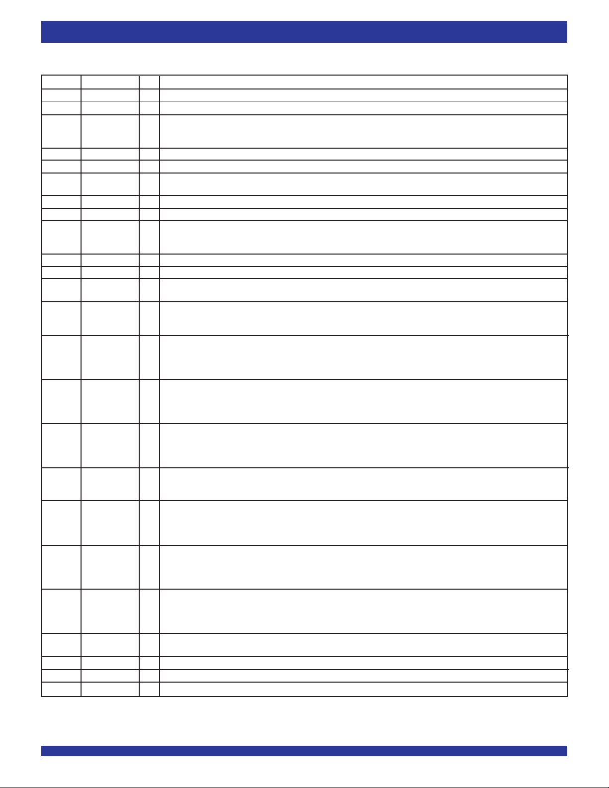
PIN DESCRIPTION
Symbol Name I/O Description
D
A0-DA17 Data A I/O Data inputs & outputs for the 18-bit Port A bus.
A Chip Select A I Port A is accessed when CSA is LOW. Port A is inactive if CSA is HIGH.
CS
A Read/Write A I
R/W
CLKA Clock A I CLKA is typically a free running clock. Data is read or written into Port A on the rising edge of CLKA.
A Enable A I
EN
OEA
0, A1, A2 Addresses I When CSA is asserted, A0, A1, A2 and R/WA are used to select one of six internal resources.
A
B0-DB17 Data B I/O Data inputs & outputs for the 18-bit Port B bus.
D
R/W
Output Enable A
B Read/Write B I
CLKB Clock B I
ENB Enable B I
OEB
EF
Output Enable B
AB A→B Empty O When EFAB is LOW, the A→B FIFO is empty and further data reads from Port B are inhibited. When EFAB is HIGH, the FIFO is
Flag not empty. EF
AB A→B O When PAEAB is LOW, the A→B FIFO is almost-empty. An almost-empty FIFO contains less than or equal to the offset
PAE
Programmable programmed into PAE
Almost-Empty default offset value for PAE
Flag
AB A→B O When PAFAB is LOW, the A→B FIFO is almost-full. An almost-full FIFO contains greater than the FIFO depth minus the offset
PAF
Programmable programmed into PAF
Almost-Full offset in PAF
Flag
AB A→B Full Flag O
FF
EFBA B→A Empty O When EFBA is LOW, the B→A FIFO is empty and further data reads from Port A are inhibited. When EFBA is HIGH, the FIFO
Flag is not empty. EF
BA B→A O When PAEBA is LOW, the B→A FIFO is almost-empty. An almost-empty FIFO contains less than or equal to the offset
PAE
Programmable programmed into PAE
Almost-Empty default offset value for PAE
Flag
BA B→A O When PAFBA is LOW, the B→A FIFO is almost-full. An almost-full FIFO contains greater than the FIFO depth minus the offset
PAF
Programmable programmed into PAF
Almost-Full offset in PAF
Flag
BA B→A Full Flag O
FF
BYPB Port B Bypass O
Flag bypass mode. If BYP
RS Reset I A LOW on this pin will perform a reset of all synchronous BiFIFO functions.
CC Power There are three +5V power pins for the PLCC and two for the TQFP.
V
GND Ground There are seven ground pins for the PLCC and four for the TQFP.
This pin controls the read or write direction of Port A. If R/WA is LOW, Data A input data is written into Port A. If R/WA is HIGH,
A
Data A output data is read from Port A. In bypass mode, when R/W
A
is HIGH, message is read from B→A output register.
R/W
is LOW, message is written into A→B output register. If
When ENA is LOW, data can be read or written to Port A. When ENA is HIGH, no data transfers occur.
I When R/WA is HIGH, Port A is an output bus and OEA controls the high-impedance state of DA0-DA17. If OEA is HIGH, Port A is
in a high-impedance state. If OE
A is LOW while CSA is LOW and R/WA is HIGH, Port A is in an active (low-impedance) state.
This pin controls the read or write direction of Port B. If R/WB is LOW, Data B input data is written into Port B. If R/WB is HIGH,
B
Data B output data is read from Port B. In bypass mode, when R/W
B
is HIGH, message is read from A→B output register.
R/W
is LOW, message is written into B→A output register. If
Clock B is typically a free running clock. Data is read or written into Port B on the rising edge of CLKB.
When ENB is LOW, data can be read or written to Port B. When ENB is HIGH, no data transfers occur.
I When R/WB is HIGH, Port B is an output bus and OEB controls the high-impedance state of DB0-DB17. If OEB is HIGH, Port B is
in a high-impedance state. If OE
AB is synchronized to CLKB. In the bypass mode, EFAB HIGH indicates that data DA0-DA17 is available for passing
through. After the data D
AB Register. When PAEAB is HIGH, the A→B FIFO contains more than offset in PAEAB Register. The
AB Register. When PAFAB is HIGH, the A→B FIFO contains less than or equal to the depth minus the
AB Register. The default offset value for PAFAB Register is 8. PAFAB is synchronized to CLKA.
When FFAB is LOW, the A→B FIFO is full and further data writes into Port A are inhibited. When FF
AB
full. FF
FF
is synchronized to CLKA. In bypass mode, FFAB tells Port A that a message is waiting in Port B’s output register. If
AB
is LOW, a bypass message is in the register. If FF
B is LOW while R/WB is HIGH, Port B is in an active (low-impedance) state.
B0-DB17 has been read, EFAB goes LOW.
AB Register is 8. PAEAB is synchronized to CLKB.
AB
is HIGH, Port B has read the message and another message can be
AB
is HIGH, the FIFO is not
written into Port A.
BA is synchronized to CLKA. In the bypass mode, EFBA HIGH indicates that data DB0-DB17 is available for
passing through. After the data D
BA Register. When PAEBA is HIGH, the B→A FIFO contains more than offset in PAEBA Register. The
BA Register. When PAFBA is HIGH, the B→A FIFO contains less than or equal to the depth minus the
BA Register. The default offset value for PAFBA Register is 8. PAFBA is synchronized to CLKB.
A0-DA17 has been read, EFBA goes LOW on the following cycle.
BA Register is 8. PAEBA is synchronized to CLKA.
When FFBA is LOW, the B→A FIFO is full and further data writes into Port B are inhibited. When FFBA is HIGH, the FIFO is
BA
not full. FF
BA
FF
is synchronized to CLKB. In bypass mode, FFBA tells Port B that a message is waiting in Port A’s output register. If
is LOW, a bypass message is in the register. If FFBA is HIGH, Port A has read the message and another message can be
written into Port B.
This flag informs Port B that the synchronous BiFIFO is in bypass mode. When BYPB is LOW, Port A has placed the FIFO into
B
is HIGH, the synchronous BiFIFO passes data into memory. BYPB is synchronized to CLKB.
3
Page 4
IDT72605/72615 CMOS SYNCBiFIFO™
256 x 18x 2 and 512 x 18 x 2
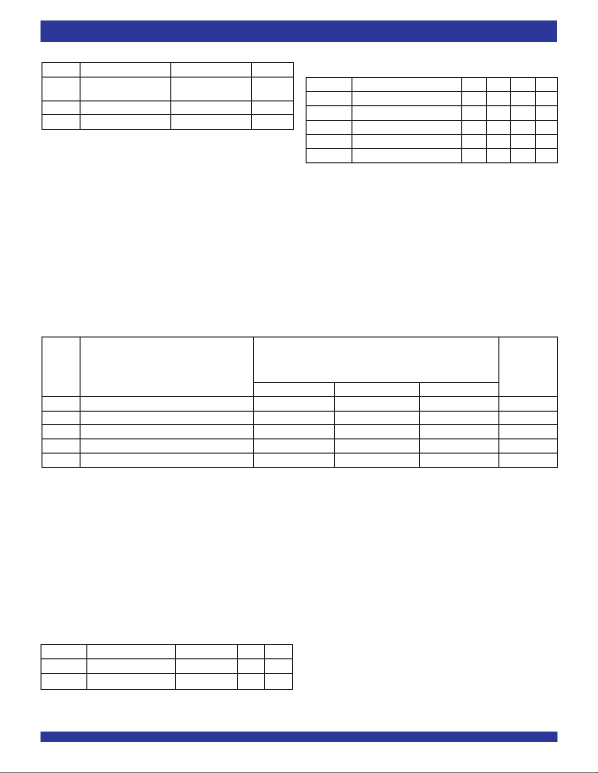
ABSOLUTE MAXIMUM RATINGS
(1)
Symbol Rating Industrial Unit
TERM Terminal Voltage with –0.5 to +7.0 V
V
Respect to Ground
STG Storage Temperature –55 to +125 °C
T
OUT DC Output Current –50 to +50 mA
I
NOTE:
1. Stresses greater than those listed under ABSOLUTE MAXIMUM RATINGS may cause
permanent damage to the device. This is a stress rating only and functional operation
of the device at these or any other conditions above those indicated in the operational
sections of this specification is not implied. Exposure to absolute maximum rating
conditions for extended periods may affect reliability.
INDUSTRIAL TEMPERATURE RANGE
RECOMMENDED DC OPERATING
CONDITIONS
SYMBOL PARAMETER MIN. TYP. MAX. UNIT
CC Supply Voltage 4.5 5.0 5.5 V
V
GND Supply Voltage 0 0 0 V
IH Input High Voltage 2.0 — — V
V
(1)
IL
V
A Operating Temperature -40 — 85 °C
T
NOTE:
1. 1.5V undershoots are allowed for 10ns once per cycle.
Input Low Voltage — — 0.8 V
DC ELECTRICAL CHARACTERISTICS
(Industrial: VCC = 5V ± 10%, TA = -40°C to +85°C)
IDT72615L
IDT72605L
Industrial
CLK = 20, 25, 35, 50ns
t
Symbol Parameter Min. Typ. Max. Unit
(1)
LI
I
LO
I
OH Output Logic "1" Voltage IOUT = –2mA 2.4 — — V
V
OL Output Logic "0" Voltage IOUT = 8mA — — 0.4 V
V
CC
I
NOTES:
1. Measurements with 0.4V ≤ V
2. OEA, OEB ≥ V
3. Tested with outputs open (I
Input Leakage Current (Any Input) – 1 — 1 µA
(2)
Output Leakage Current –1 0 — 10 µA
(3)
Active Power Supply Current — — 230 mA
IH; 0.4 ≤ VOUT ≤ VCC.
IN ≤ VCC.
OUT = 0). Testing frequency f=20MHz.
CAPACITANCE (TA = +25°C, F = 1.0MHz)
Symbol Parameter Conditions Max. Unit
(2)
IN
C
OUT
C
NOTES:
1. With output deselected.
2. Characterized values, not currently tested.
Input Capacitance VIN = 0V 10 pF
(1,2)
Output Capacitance VOUT = 0V 10 pF
4
Page 5
IDT72605/72615 CMOS SYNCBiFIFO™
256 x 18x 2 and 512 x 18 x 2 INDUSTRIAL TEMPERATURE RANGE
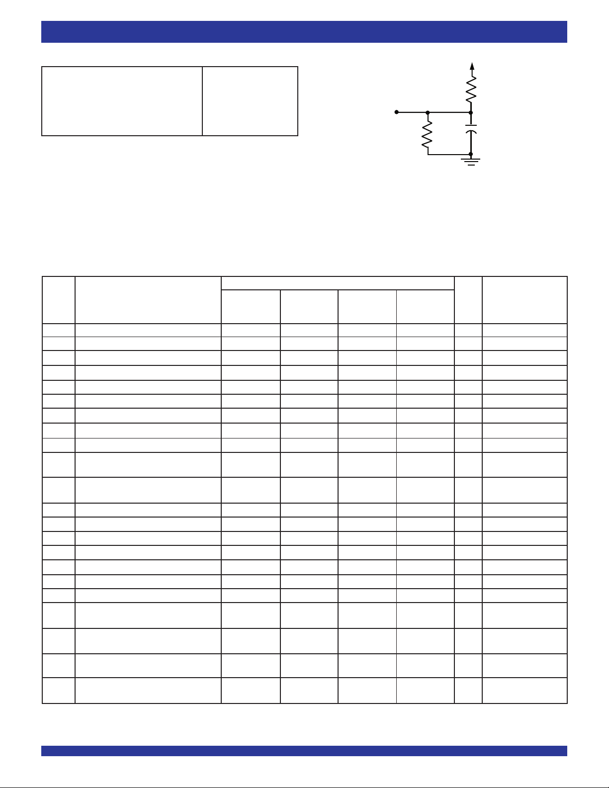
AC TEST CONDITIONS
+5V
In Pulse Levels GND to 3.0V
Input Rise/Fall Times 3ns
1.1KΩ
Input Timing Reference Levels 1.5V
Output Reference Levels 1.5V
Output Load See Figure 2
D.U.T.
680Ω
30pF*
2704 drw 04
or equivalent circuit
Figure 2. Output Load
* Includes jig and scope capacitances.
AC ELECTRICAL CHARACTERISTICS
(Industrial: VCC = 5V ± 10%, TA = -40°C to +85°C)
Industrial
IDT72615L20 IDT72615L25 IDT72615L35 IDT72615L50
IDT72605L20 IDT72605L25 IDT72605L35 IDT72605L50
Symbol Parameter Min. Max. Min. Max. Min. Max. Min. Max. Unit Timing Figures
CLK Clock frequency — 50 — 4 0 — 28 — 20 MHz —
f
CLK Clock cycle time 2 0 — 25 — 35 — 50 — ns 4,5,6,7
t
CLKH Clock HIGH time 8 — 10 — 14 — 20 — ns 4,5,6,7,12,13,14,15
t
CLKL Clock LOW time 8 — 1 0 — 1 4 — 2 0 — ns 4,5,6,7,12,13,14,15
t
RS Reset pulse width 2 0 — 25 — 35 — 5 0 — ns 3
t
RSS Reset setup time 12 — 1 5 — 2 1 — 30 — ns 3
t
RSR Reset recovery time 1 2 — 1 5 — 21 — 3 0 — ns 3
t
RSF Reset to flags in initial state — 27 — 28 — 35 — 50 ns 3
t
A Data access time 3 10 3 1 5 3 21 3 25 ns 5,7,8,9,10,11
t
CS Control signal setup time
t
CH Control signal hold time
t
DS Data setup time 6 — 6 — 8 — 10 — ns 4,6,8,9,10,11
t
DH Data hold time 1 — 1 — 1 — 1 — ns 4,6
t
OE Output Enable LOW to output data valid
t
OLZ Output Enable LOW to data bus at Low-Z
t
OHZ Output Enable HIGH to data bus at High-Z
t
FF Clock to Full Flag time — 1 0 — 15 — 2 1 — 30 ns 4,6,10,11
t
EF Clock to Empty Flag time — 10 — 1 5 — 2 1 — 30 ns 5,7,8,9,10,11
t
PAE Clock to Programmable — 12 — 15 — 2 1 — 3 0 n s 12,14
t
Almost-Empty Flag time
PAF Clock to Programmable — 1 2 — 1 5 — 21 — 30 ns 13,15
t
Almost-Full Flag time
SKEW1 Skew between CLKA & CLKB 10 — 12 — 17 — 2 0 — ns 4,5,6,7,8,9,10,11
t
for Empty/Full Flags
tSKEW2 Skew between CLKA & CLKB 17 — 1 9 — 25 — 34 — ns 4, 7,12,13,14,15
for Programmable Flags
NOTES:
1. Control signals refer to CS
2. Minimum values are guaranteed by design.
(1)
(1)
(2)
(2)
(2)
A, R/WA, ENA, A2, A1, A0, R/WB, ENB.
6 — 6 — 8 — 10 — ns 4,5,6,7,8,9,10,11,
1 — 1 — 1 — 1 — ns 4,5,6,7,10,11,12,
3 10 3 13 3 2 0 3 28 ns 5,7,8,9,10,11
(2)
0 — 0 — 0 — 0 — ns 5,7,8,9,10,11
(2)
3 10 3 13 3 20 3 28 ns 5,7,10,11
12, 13,14,15
13, 14,15
5
Page 6
IDT72605/72615 CMOS SYNCBiFIFO™
256 x 18x 2 and 512 x 18 x 2
INDUSTRIAL TEMPERATURE RANGE
FUNCTIONAL DESCRIPTION
IDTs SyncBiFIFO is versatile for both multiprocessor and peripheral
applications. Data can be stored or retrieved from two sources simultaneously.
The SyncBiFIFO has registers on all inputs and outputs. Data is only
transferred into the I/O registers on clock edges, hence the interfaces are
synchronous. Two Dual-Port FIFO memory arrays are contained in the
SyncBiFIFO; one data buffer for each direction. Each port has its own
independent clock. Data transfers to the I/O registers are gated by the enable
signals. The transfer direction for each port is controlled independently by a
read/write signal. Individual output enable signals control whether the SyncBiFIFO
is driving the data lines of a port or whether those data lines are in a highimpedance state. The processor connected to Port A of the BiFIFO can send
or receive messages directly to the Port B device using the 18-bit bypass path.
The SyncBiFIFO can be used in multiples of 18-bits. In a 36- to 36-bit
configuration, two SyncBiFIFOs operate in parallel. Both devices are programmed simultaneously, 18 data bits to each device. This configuration can
be extended to wider bus widths (54- to 54-bits, 72- to 72-bits, etc.) by adding
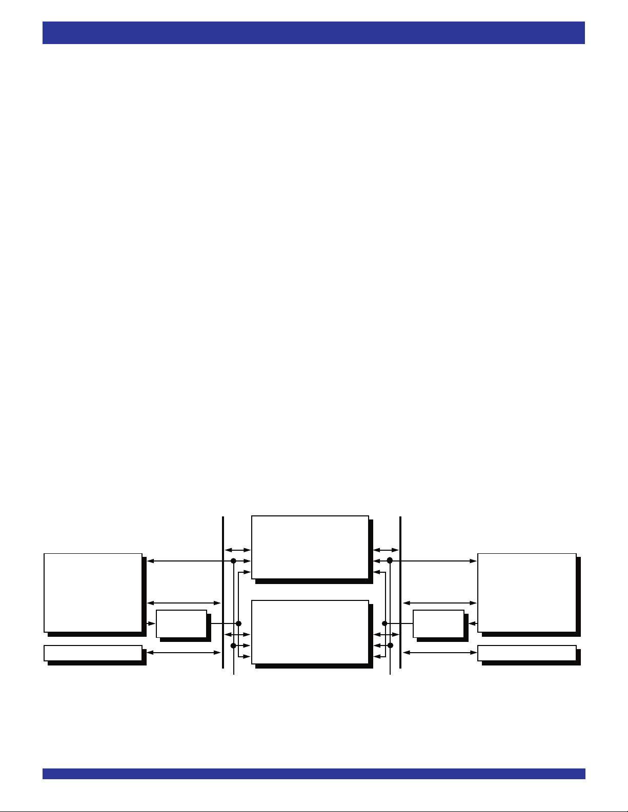
more SyncBiFIFOs to the configuration. Figure 1 shows multiple SyncBiFIFOs
configured for multiprocessor communication.
The microprocessor or microcontroller connected to Port A controls all
operations of the SyncBiFIFO. Thus, all Port A interface pins are inputs driven
by the controlling processor. Port B interfaces with a second processor. The
Port B control pins are inputs driven by the second processor.
RESET
Reset is accomplished whenever the Reset (RS) input is taken to a LOW state
A, ENA and ENB HIGH. During reset, both internal read and write
with CS
pointers are set to the first location. A reset is required after power up before a
write operation can take place. The A→B and B→A FIFO Empty Flags (EFAB,
EFBA) and Programmable Almost-Empty flags (PAEAB, PAEBA) will be set to
LOW after tRSF. The A→B and B→A FIFO Full Flags (FFAB, FFBA) and
Programmable Almost- Full flags (PAFAB, PAFBA) will be set to HIGH after tRSF.
After the reset, the offsets of the Almost-Empty flags and Almost- Full flags for the
A→B and B→A FIFO offset default to 8.
PORT A INTERFACE
The SyncBiFIFO is straightforward to use in micro-processor-based
systems because each port has a standard microprocessor control set. Port A
interfaces with microprocessor through the three address pins (A
2-A0) and a
Chip Select CSA pins. When CSA is asserted, A2,A1,A0 and R/WA are used
to select one of six internal resources (Table 1).
With A2=0 and A1=0, A0 determines whether data can be read out of output
register or be written into the FIFO (A0=0), or the data can pass through the
FIFO through the bypass path (A0=1).
2=1, four programmable flags (two A→B FIFO programmable flags
With A
and two B→A FIFO programmable flags) can be selected: the A→B FIFO
Almost-Empty flag Offset (A1=0, A0=0), A→B FIFO Almost-Full flag Offset
(A
1=0, A0=1), B→A FIFO Almost-Empty flag Offset (A1=1, A0=0), B→A FIFO
Almost-Full flag Offset (A1=1, A0=1).
Port A is disabled when CSA is deasserted and data A is in high-impedance
state.
BYPASS PATH
The bypass paths provide direct communication between Port A and Port
B. There are two full 18-bit bypass paths, one in each direction. During a bypass
operation, data is passed directly between the input and output registers, and
the FIFO memory is undisturbed.
Port A initiates and terminates all bypass operations. The bypass flag, BYP
is asserted to inform Port B that a bypass operation is beginning. The bypass
flag state is controlled by the Port A controls, although the BYPB signal is
synchronized to CLKB. So, BYPB is asserted on the next rising edge of CLKB
when A2A1A0=001and CS A is LOW. When Port A returns to normal FIFO mode
(A2A1A0=000 or CSA is HIGH), BYPB is deasserted on the next CLKB rising
edge.
Once the SyncBiFIFO is in bypass mode, all data transfers are controlled
by the standard Port A (R/WA, CLKA, ENA, OEA) and Port B (R/WB, CLKB,
ENB, OEB) interface pins. Each bypass path can be considered as a one word
deep FIFO. Data is held in each input register until it is read. Since the controls
B,
CLK
MICROPROCESSOR
NOTES:
1. Upper SyncBiFIFO only is used in 18- to 18-bit configuration.
2. Control A consists of R/W
A
RAM A
DATA
ADDR, I/0
A, ENA, OEA, CSA, A2, A 1, A0. Control B consists of R/WB, ENB, OEB.
CONTROL
LOGIC
SYSTEM
CLOCK A
Figure 1. 36- to 36-bit Processor Interface Configuration
SYNCBIFIFO
DATA A
CLK
A
CONTROL A
SYNCBIFIFO
DATA A
A
CLK
CONTROL A
IDT
DATA B
CONTROL B
IDT
CONTROL B
6
CLK
DATA B
CLK
B
B
SYSTEM
CLOCK B
CONTROL
LOGIC
CLK
MICROPROCESSOR
B
DATA
ADDR, I/0
RAM B
2704 drw 05
Page 7
IDT72605/72615 CMOS SYNCBiFIFO™
256 x 18x 2 and 512 x 18 x 2 INDUSTRIAL TEMPERATURE RANGE
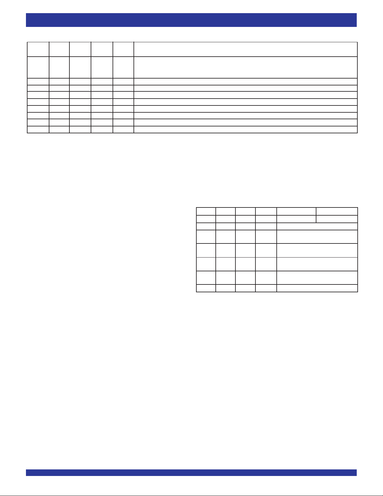
TABLE 1 PORT A OPERATION CONTROL SIGNALS
Data A
CS
A R/WA ENA OEA I/O Port A Operation
0 0 0 0 I Data A is written on CLK
that even though OE
a high-impedance state.
0 0 0 1 I Data A is written on CLKA ≠
0 0 1 X I Data A is ignored
0 1 0 0 O Data is read
0 1 0 1 O Data is read
0 1 1 0 O Output register does not change
0 1 1 1 O Output register does not change
1 0 X X I Data A is ignored
1 1 X X O Data A is high-impedance
NOTES:
1. When A
2. Regardless of the condition of A
3. If CS
2A1A0 = 000, the next B→A FIFO value is read out of the output register and the read pointer advances. If A2A1A0 = 001, the bypass path is selected and bypass
data from the Port B input register is read from the Port A output register. If A
register.
2A1A0, the data in the Port A output register does not change and the B→A read pointer does not advance.
A# is HIGH, then BYPB is HIGH. No bypass occur under this condition.
(1)
from RAM array to output register on CLKA ≠, Data A is low-impedance
(1)
from RAM array to output register on CLKA ≠, Data A is high-impedance
A ≠. This write cycle immediately following low-impedance cycle is prohibited. Note
A = 0, a LOW logic level on R/WA, once qualified by a rising edge on CLKA, will put Data A into
(2)
, Data A is low-impedance
(2)
(3)
2A1A00 = 1XX, a flag offset register is selected and its offset is read out through Port A output
, Data A is high-impedance
(3)
of each port operate independently, Port A can be reading bypass data at the
same time Port B is reading bypass data.
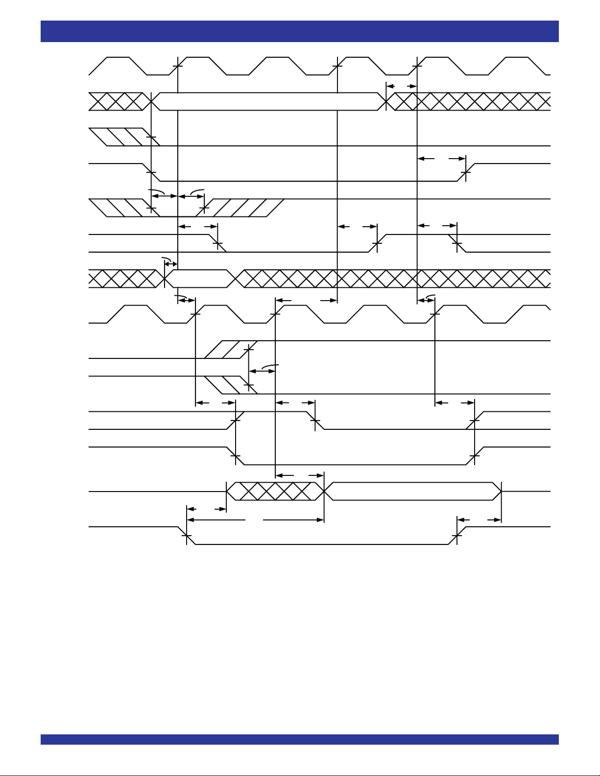
When R/WA and ENA is LOW, data on pins DA0-DA17 is written into Port
A input register. Following the rising edge of CLKA for this write, the A→B Full
Flag (FFAB) goes LOW. Subsequent writes into Port A are blocked by internal
logic until FFAB goes HIGH again. On the next CLKB rising edge, the A→B
Empty Flag (EFAB) goes HIGH indicating to Port B that data is available. Once
R/WB is HIGH and ENB is LOW, data is read into the Port B output register. OEB
still controls whether Port B is in a high-impedance state. When OEB is LOW,
the output register data appears at DB0-DB17. EFAB goes LOW following the
CLKB rising edge for this read. FFAB goes HIGH on the next CLKA rising edge,
letting Port A know that another word can be written through the bypass path.
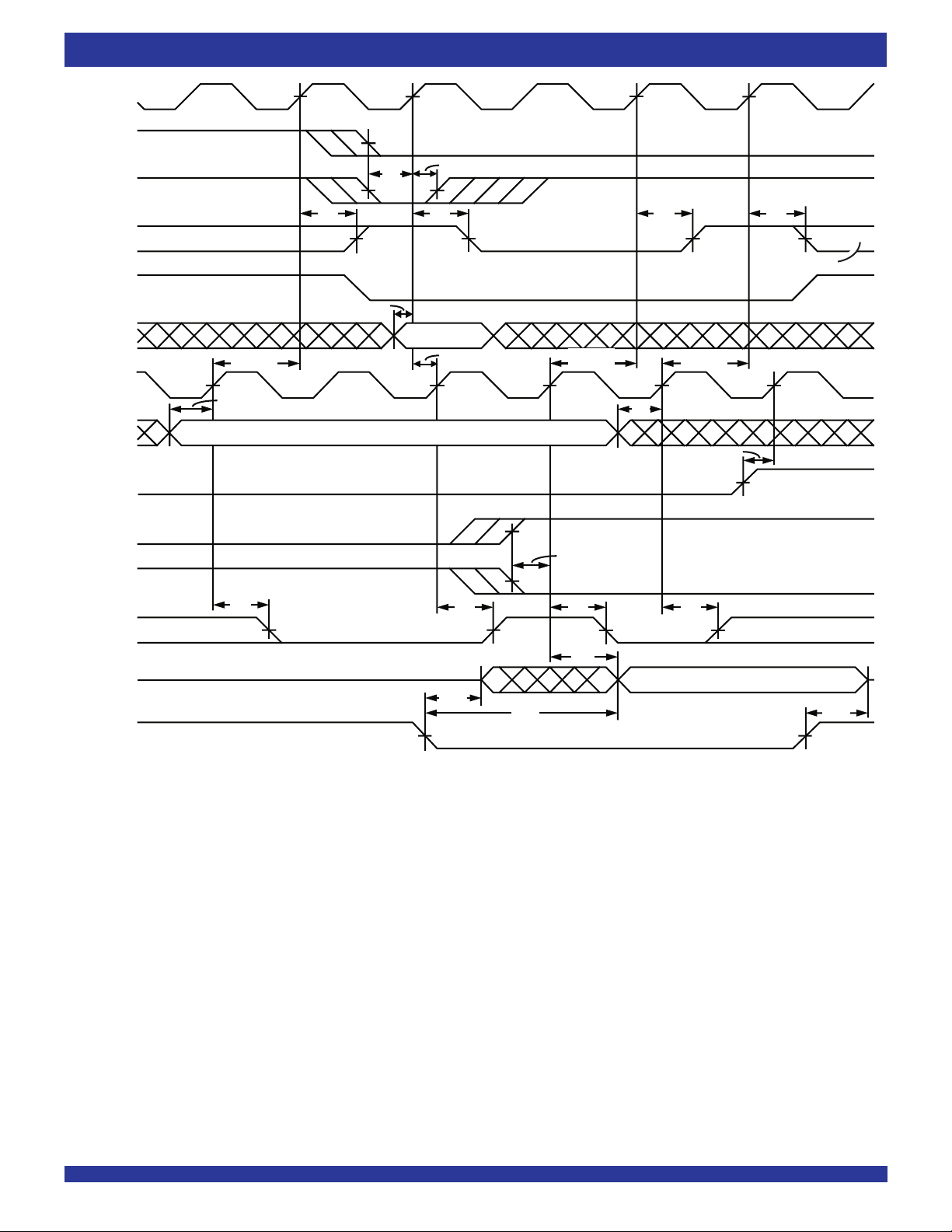
Bypass data transfers from Port B to Port A work in a similar manner with
EFBA and FFBA indicating the Port A output register state.
When the Port A address changes from bypass mode (A2A1A0=001) to
FIFO mode (A2A1A0=000) on the rising edge of CLKA, the data held in the Port
B output register may be overwritten. Unless Port A monitors the BYPB pin and
waits for Port B to clock out the last bypass word, data from the A→B FIFO will
overwrite data in the Port B output register. BYPB will go HIGH on the rising
edge of CLKB signifying that Port B has finished its last bypass operation. Port
B must read any bypass data in the output register on this last CLKB clock or
it is lost and the SyncBiFIFO returns to FIFO operations. It is especially important
to monitor BYPB when CLKB is much slower than CLKA to avoid this condition.
BYPB will also go HIGH after CSA is brought HIGH; in this manner the Port B
bypass data may also be lost.
Since the Port A processor controls CSA and the bypass mode, this scenario
can be handled for B→A bypass data. The Port A processor must be set up
to read the last bypass word before leaving bypass mode.
PORT A CONTROL SIGNALS
The Port A control signals pins dictate the various operations shown in Table
2. Port A is accessed when CS
A is LOW, and is inactive if CSA is HIGH. R/
WA and ENA lines determine when Data A can be written or read. If R/WA and
ENA are LOW, data is written into input register on the LOW-to-HIGH transition
of CLKA. If R/WA is HIGH and OEA is LOW, data comes out of bus and is read
from output register into three-state buffer. Refer to pin descriptions for more
information.
TABLE 2 ACCESSING PORT A RESOURCES USING CS
CSA A2 A1 A0 Read Write
0000 B→A FIFO A→B FIFO
0 0 0 1 18-bit Bypass Path
0100 A→B FIFO Almost-Empty
0101 A→B FIFO Almost-Full
0110 B→A FIFO Almost-Empty
0111 B→A FIFO Almost-Full
1 X X X Port A Disabled
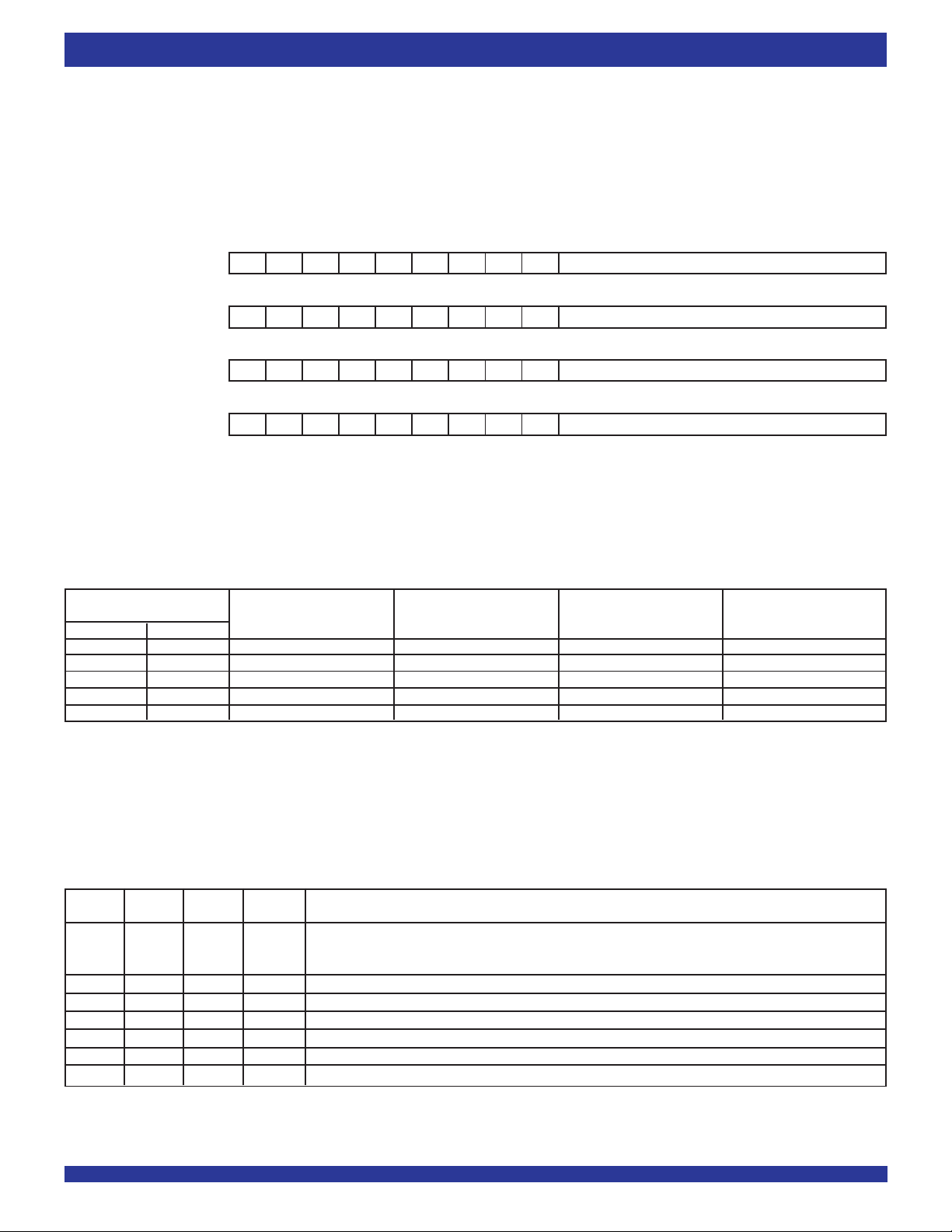
PROGRAMMABLE FLAGS
The IDT SyncBiFIFO has eight flags: four flags for A→B FIFO (EF
PAEAB, PAFAB, FFAB), and four flags for B→A FIFO (EFBA, PAEBA, PAFBA,
FFBA). The Empty and Full flags are fixed, while the Almost-Empty and Almost-
Full offsets can be set to any depth through the Flag Offset Registers (see Table
3). The flags are asserted at the depths shown in the Flag Truth Table (Table
4). After reset, the programmable flag offsets are set to 8. This means the AlmostEmpty flags are asserted at Empty +8 words deep, and the Almost-Full flags are
asserted at Full -8 words deep.
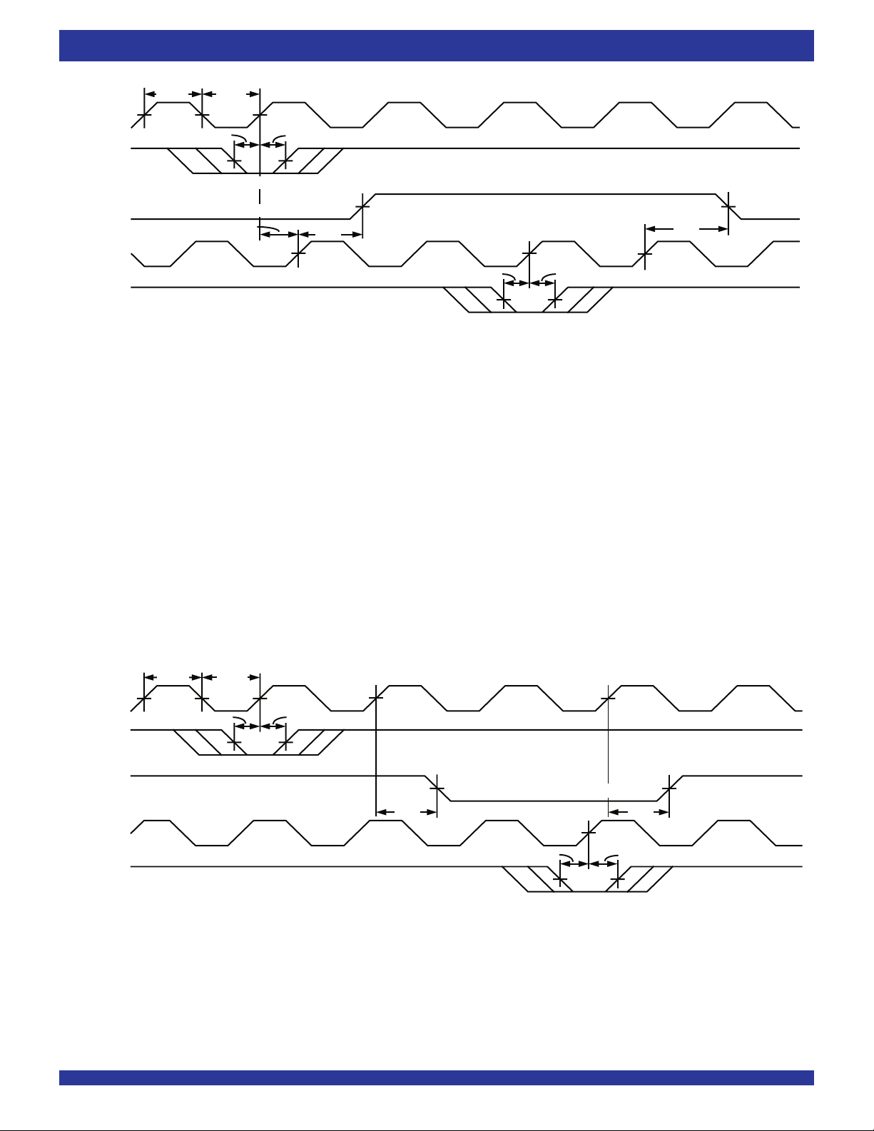
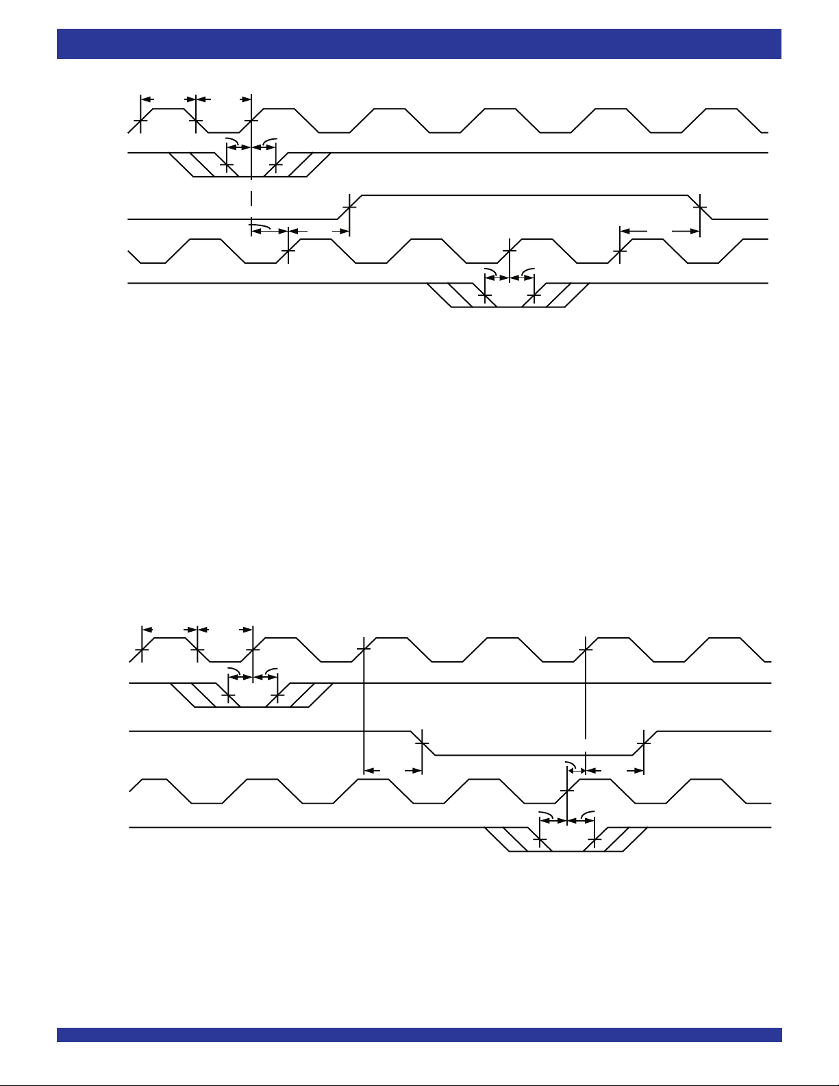
The PAEAB is synchronized to CLKB, while PAEAB is synchronized to CLKA;
and PAEBA is synchronized to CLKA, while PAEBA is synchronized to CLKB.
If the minimum time (tSKEW2) between a rising CLKB and a rising CLKA is met,
the flag will change state on the current clock; otherwise, the flag may not change
state until the next clock rising edge. For the specific flag timings, refer to Figures
12-15.
PORT B CONTROL SIGNALS
The Port B control signal pins dictate the various operations shown in Table
5. Port B is independent of CS
A. R/WB and ENB lines determine when Data
A, A2, A1, AND A0
Flag Offset
Flag Offset
Flag Offset
Flag Offset
AB,
7
Page 8
IDT72605/72615 CMOS SYNCBiFIFO™
256 x 18x 2 and 512 x 18 x 2
INDUSTRIAL TEMPERATURE RANGE
can be written or read in Port B. If R/WB and ENB are LOW, data is written into
input register, and on LOW-to-HIGH transition of CLK
B data is written into input
register and the FIFO memory. If R/WB is HIGH and OEB is LOW, data comes
if R/W
B is LOW, bypass messages are transferred into B→A output register.
A is HIGH, bypass messages are transferred into A→B output register.
If R/W
Refer to pin descriptions for more information.
out of bus and is read from output register into three-state buffer. In bypass mode,
TABLE 3 FLAG OFFSET REGISTER FORMAT
17161514131211109876543210
PAE
AB Register XXXXXXXXX A→B FIFO Almost-Empty Flag Offset
17161514131211109876543210
AB Register XXXXXXXXX A→B FIFO Almost-Full Flag Offset
PAF
17161514131211109876543210
BA Register XXXXXXXXX B→A FIFO Almost-Empty Flag Offset
PAE
17161514131211109876543210
BA Register XXXXXXXXX B→A FIFO Almost-Full Flag Offset
PAF
NOTE:
1. Bit 8 must be set to 0 for the IDT72605 (256 x 18) Synchronous BiFIFO.
TABLE 4 INTERNAL FLAG TRUTH TABLE
Number of Words
in FIFO
From To EF PAE PAF FF
0 0 LOW LOW HIGH HIGH
1 n HIGH LOW HIGH HIGH
n+1 D-(m+1) HIGH HIGH HIGH HIGH
D-m D-1 HIGH HIGH LOW HIGH
D D HIGH HIGH LOW LOW
NOTE:
1. n = Programmable Empty Offset (PAE
m = Programmable Full Offset (PAF
D = FIFO Depth (IDT72605 = 256 words, IDT72615= 512 words)
AB Register or PAEBA Register)
AB Register or PAFBA Register)
TABLE 5 PORT B OPERATION CONTROL SIGNALS
Data B
B ENB OEB I/O Port B Operation
R/W
000I
0 0 1 I Data B is written on CLKB ↑.
0 1 X I Data B is ignored
1 0 0 O Data is read
1 0 1 O Data is read
1 1 0 O Output register does not change
1 1 1 O Output register does not change
NOTES:
1. When A
2. Regardless of the condition of A2A1A0, the data in the Port B output register does not change and the A→B read pointer does not advance.
2A1A0 = 000 or 1XX, the next A→B FIFO value is read out of the output register and the read pointer advances. If A2A1A0 = 001, the bypass path is selected and
bypass data is read from the Port B output register.
Data B is written on CLKB ↑. This write cycle immediately following output low-impedance cycle is prohibited. Note
that even though OE
B = 0, a LOW logic level on R/WB, once qualified by a rising edge on CLKB, will put Data B into a high-
impedance state.
(1)
from RAM array to output register on CLKB ≠ Data B is low-impedance
(1)
from RAM array to output register on CLKB ≠, Data B is high- impedance
(2)
, Data B is low-impedance
(2)
, Data B is high-impedance
8
Page 9
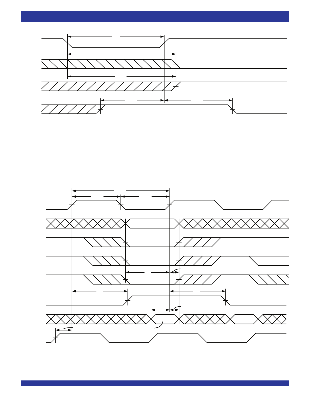
IDT72605/72615 CMOS SYNCBiFIFO™
256 x 18x 2 and 512 x 18 x 2 INDUSTRIAL TEMPERATURE RANGE
RS
t
RS
RSF
EFAB,
t
PAEAB,
EFBA,
PAEBA
RSF
EFAB,
t
PAEAB,
EFBA,
PAEBA
CSA,
ENA
ENB
RSS
t
,
RSR
t
2704 drw 06
Figure 3. Reset Timing
A0, A
D
A0-DA17
CLK
1, A2
R/
CS
EN
FF
W
AB
tCLK
tCLKH
A
A
A
A
tFF
tSKEW1
DATA IN VALID
tCLKL
tCS
tDS
tCH
NO OPERATION
tFF
tDH
CLK
B
READ
Figure 4. Port A (A
NO READ OPERATION
→→
→
B) Write Timing
→→
2704 drw 07
9
Page 10
IDT72605/72615 CMOS SYNCBiFIFO™
256 x 18x 2 and 512 x 18 x 2
CLK
A
A0, A
1, A2
R/
W
A
CS
A
t
CS
INDUSTRIAL TEMPERATURE RANGE
t
CLK
t
CLKH
t
CH
t
CLKL
D
A0-DA17
CLK
CLK
EF
EN
OE
NO OPERATION
t
EF
BA
A
t
EF
t
A
VALID DATA
t
OLZ
t
OE
A
B
t
CLKH
B
NO WRITE
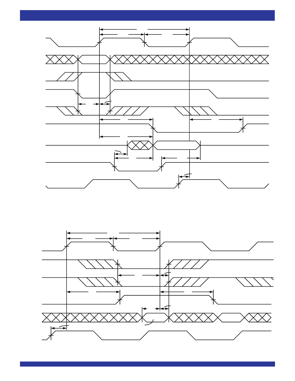
Figure 5. Port A (B
t
CLK
t
CLKL
→→
→
A) Read Timing
→→
t
OHZ
t
SKEW1
WRITE
2704 drw 08
R/
D
B0-DB17
CLK
EN
FF
W
BA
B
t
t
CH
DH
NO OPERATION
t
FF
2704 drw 09
t
CS
B
t
FF
t
DS
t
SKEW1
A
READ NO READ OPERATION
DATA IN VALID
Figure 6. Port B (B
→→
→
A) Write Timing
→→
10
Page 11
IDT72605/72615 CMOS SYNCBiFIFO™
256 x 18x 2 and 512 x 18 x 2 INDUSTRIAL TEMPERATURE RANGE
t
CLK
t
OE
t
CLKL
NO OPERATION
VALID DATA
t
SKEW1
t
OHZ
WRITE
EF
t
2704 drw 10
CLK
R/
D
B0-DB17
CLK
EF
OE
EN
t
CLKH
B
W
B
t
t
OLZ
CH
t
EF
t
A
BA
t
CS
B
B
A
NO WRITE OPERATION
CLK
A
A0, A1, A
CSA, EN
R/
D
A0-DA17
CLK
R/
EF
D
B0-DB17
W
W
EN
OE
AB
2
A
t
CS
A
t
DS
D
0
(First Valid Write)
t
(1)
OLZ
t
SKEW1
B
B
B
B
NOTE:
1. When t
SKEW1 ≥ minimum specification, tFRL(Max.) = tCLK + tSKEW1
tSKEW1 < minimum specification, tFRL(Max.) = 2tCLK + tSKEW1 or tCLK + tSKEW1
The Latency Timing applies only at the Empty Boundary (EF = LOW).
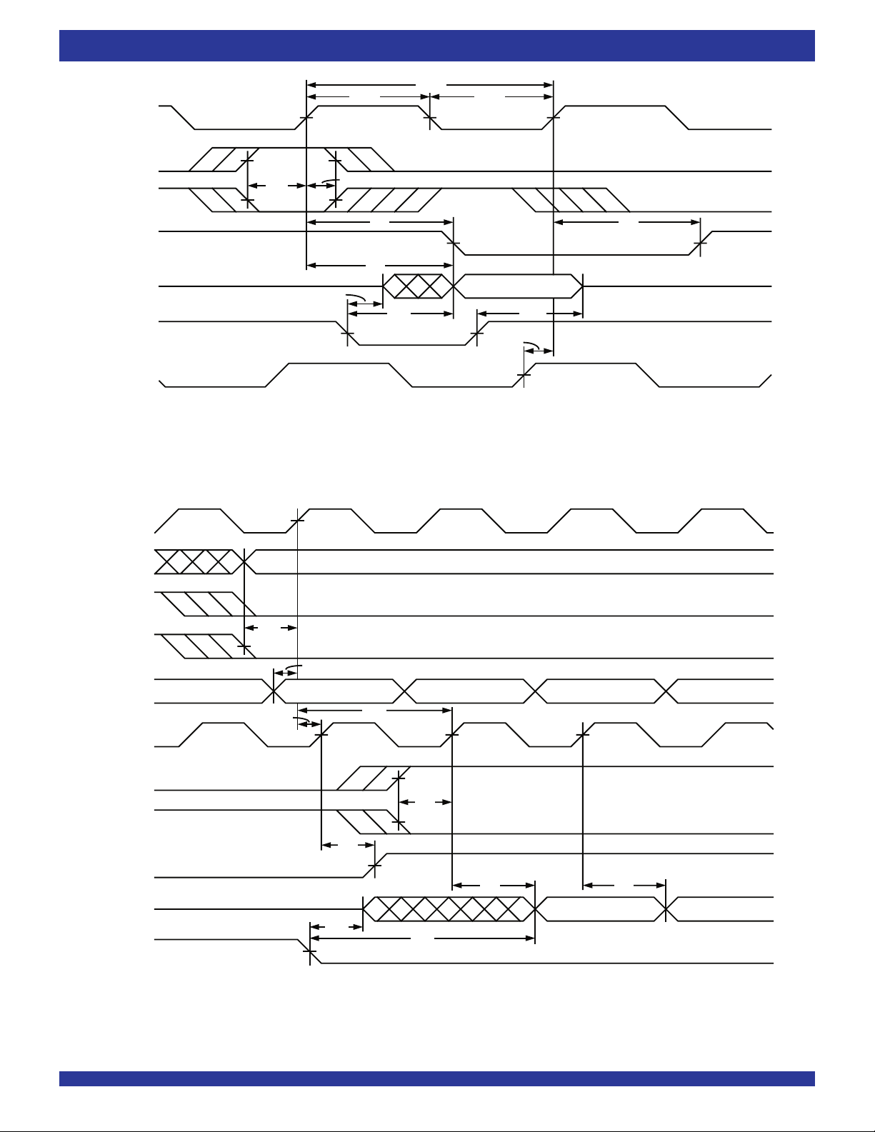
Figure 8. A
→→
→
B First Data Word Latency after Reset for Simultaneous Read and Write
→→
Figure 7. Port B (A
t
FRL
t
CS
t
EF
t
OE
→→
→
B) Read Timing
→→
D
1
t
A
D
2
t
A
D
0
D
3
D
1
2704 drw 11
11
Page 12
IDT72605/72615 CMOS SYNCBiFIFO™
256 x 18x 2 and 512 x 18 x 2
CLK
B
R/
W
B
t
CS
EN
B
D
B0-DB17
t
SKEW1
CLK
A
t
DS
D
0
(First valid write)
(1)
t
FRL
INDUSTRIAL TEMPERATURE RANGE
D
1
D
2
D
3
A0, A1, A
CSA, EN
R/
W
2
A
A
t
EF
BA
D
A0-DA17
t
OLZ
OE
A
NOTE:
1. When t
SKEW1 ≥ minimum specification, tFRL(Max.) = tCLK + tSKEW1
tSKEW1 < minimum specification, tFRL(Max.) = 2tCLK + tSKEW1
The Latency Timing apply only at the Empty Boundary (EF = LOW).
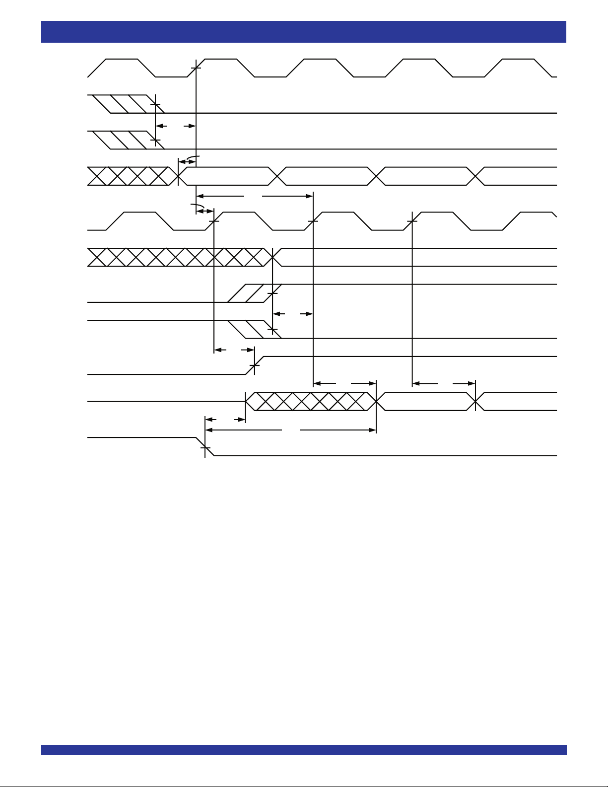
Figure 9. B
→→
→
A First Data Word Latency after Reset for Simultaneous Read and Write
→→
EF
t
CS
t
t
A
t
OE
A
D
0
D
1
2704 drw 12
12
Page 13
IDT72605/72615 CMOS SYNCBiFIFO™
256 x 18x 2 and 512 x 18 x 2 INDUSTRIAL TEMPERATURE RANGE
CLK
A
t
CS
A0, A1, A
R/
CS
EN
FF
D
A0-DA17
CLK
R/
EN
W
W
AB
2
A
A
t
CS
A
t
DS
t
CH
t
FF
A2, A1, A0 = 001
BYPASS FLAG
t
CH
t
t
FF
FF
FIFO FLAG
DATA INPUT
t
SKEW1
B
B
B
t
CS
t
SKEW1
t
SKEW1
t
EF
EF
AB
BYP
B
D
B0-DB17
t
OLZ
t
OE
OE
B
NOTES:
1. When CS
2. After the bypass operation is completed, the BYP
3. When A-side changed from bypass mode into FIFO mode, B-side only has one cycle to read the bypass data. On the next cycle, B-side will be forced back to FIFO
A is brought HIGH, A→B Bypass mode will switch to FIFO mode on the following CLKA LOW-to-HIGH transition.
B goes from LOW-to-HIGH; this will reset all bypass flags. The bypass path becomes available for the next bypass
operation.
mode.
Figure 10. A
t
EF
t
A
→→
→
B Bypass Timing
→→
BYPASS FLAGFIFO FLAG
DATA OUTPUT
t
EF
FIFO FLAG
t
OHZ
2704 drw 13
13
Page 14
IDT72605/72615 CMOS SYNCBiFIFO™
256 x 18x 2 and 512 x 18 x 2
CLK
B
R/
W
B
EN
B
FF
BA
BYP
B
INDUSTRIAL TEMPERATURE RANGE
t
t
CS
t
FF
CH
t
t
FF
t
FF
FF
BYPASS FLAG
FIFO FLAG
t
DS
D
B0-DB17
SKEW1
t
CLK
A
A0, A1, A
D
NOTES:
1. When CS
2. After the bypass operation is completed, the BYP
3. When A-side changed from bypass mode into FIFO mode, B-side only has one cycle to read the bypass data. On the next cycle, B-side will be forced back to FIFO
CS
R/
W
EN
EF
A0-DA17
OE
mode.
2
A
A
A
BA
A
A is brought HIGH, A
t
CS
A2, A1, A0 = 001
t
EF
BYPASS FLAG
→→
→
B Bypass mode will switch to FIFO mode on the following CLKA going LOW-to-HIGH.
→→
B goes from LOW-to-HIGH; this will reset all bypass flags.
DATA INPUT
t
SKEW1
t
EF
t
OLZ
t
t
CS
SKEW1
t
EF
t
CS
t
SKEW1
t
EF
t
CS
FIFO FLAGFIFO FLAG
t
A
DATA OUTPUT
t
t
OE
OHZ
2704 drw 14
Figure 11. B
→→
→
A Bypass Timing
→→
14
Page 15
IDT72605/72615 CMOS SYNCBiFIFO™
256 x 18x 2 and 512 x 18 x 2 INDUSTRIAL TEMPERATURE RANGE
t
CLK
EN
CLKH
A
A
t
t
CS
CLKL
t
CH
(R/WA = 0)
PAE
CLK
EN
(R/WB = 1)
AB
WRITE
n words in FIFO
(1)
t
SKEW2
B
A
t
PAE
n+1 words in FIFO
t
t
CS
CH
(2)
t
PAE
2704 drw 15
READ
NOTES:
1. t
SKEW2 the minimum time between a rising CLKA edge and a rising CLKB edge for PAEAB to change during that clock cycle. If the time between the rising edge of CLKA and
the rising edge of CLK
2. If a read is performed on this rising edge of the read clock, there will be Empty + (n + 1) words in the FIFO when PAE goes LOW.
B is less than tSKEW, then PAEAB may not go HIGH until the next CLKB rising edge.
CLK
EN
(R/WA = 0)
AB
PAF
CLK
EN
(R/WB = 1)
Figure 12. A
t
CLKH
A
A
t
t
CLKL
CS
t
CH
→→
→
B Programmable Almost-Empty Flag Timing
→→
(2)
WRITE
Full - (m+1) words in FIFO
t
PAF
B
B
Full - m words in FIFO
t
CS
t
PAF
t
CH
2704 drw 16
READ
NOTES:
1. t
SKEW2 is the minimum time between a rising CLKB edge and a rising CLKA edge for PAFAB to change during that clock cycle. If the time between the rising edge of CLKB
and the rising edge of CLKA is less than tSKEW2, then PAFAB may not go HIGH until the next CLKA rising edge.
2. If a write is performed on this rising edge of the write clock, there will be Full - (m + 1) words in the FIFO when PAF goes LOW.
Figure 13. A
→→
→
B Programmable Almost-Full Flag Timing
→→
15
Page 16
IDT72605/72615 CMOS SYNCBiFIFO™
256 x 18x 2 and 512 x 18 x 2
CLKH
t
CLK
B
t
CS
EN
B
t
CLKL
t
CH
INDUSTRIAL TEMPERATURE RANGE
(R/WA = 0)
WRITE
BA
PAE
CLK
EN
n words in FIFO
(1)
t
SKEW2
A
A
t
PAE
n+1 words in FIFO
t
CS
t
(2)
t
CH
PAE
(R/WA = 1)
READ
NOTES:
SKEW2 is the minimum time between a rising CLKB edge and a rising CLKA edge for PAEBA to change during that clock cycle. If the time between the rising edge of CLKB
1. t
and the rising edge of CLKA is less than tSKEW2, then PAEBA may not go HIGH until the next CLKA rising edge.
2. If a read is performed on this rising edge of the read clock, there will be Empty + (n - 1) words in the FIFO when PAE goes LOW.
2704 drw 17
CLK
EN
(R/WA = 0)
PAF
CLK
EN
(R/WA = 1)
BA
Figure 14. B
t
CLKH
B
B
t
t
CS
CLKL
t
CH
→→
→
A Programmable Almost-Empty Flag Timing
→→
(2)
WRITE
Full - (m+1) words in FIFO
t
PAF
A
A
Full - m words in FIFO
(1)
t
SKEW2
t
CS
t
PAF
t
CH
2704 drw 18
READ
NOTES:
SKEW2 is the minimum time between a rising CLKB edge and a rising CLKA edge for PAFBA to change during that clock cycle. If the time between the rising edge of CLKB
1. t
and the rising edge of CLKA is less than tSKEW2, then PAFBA may not go HIGH until the next CLKA rising edge.
2. If a write is performed on this rising edge of the write clock, there will be Full - (m + 1) words in the FIFO when PAF goes LOW.
Figure 15. B
→→
→
A Programmable Almost-Full Flag Timing
→→
16
Page 17
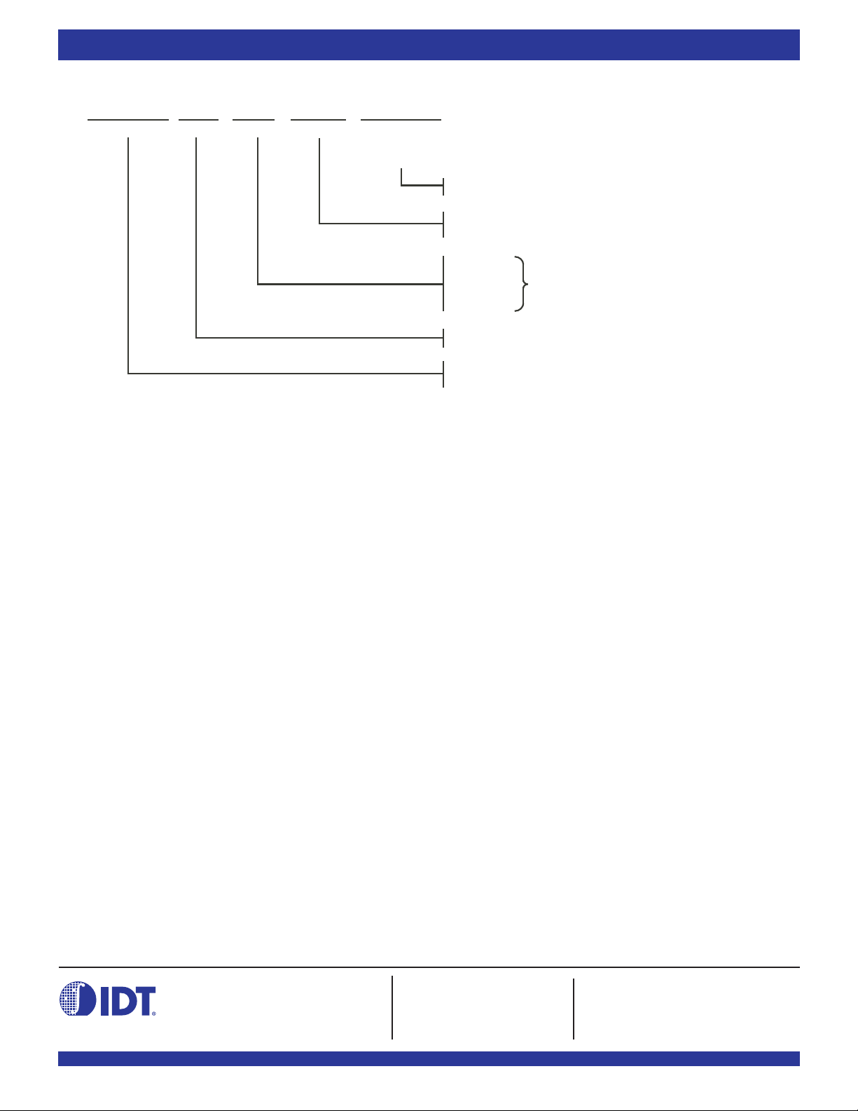
ORDERING INFORMATION
IDT
XXXXX
Device Type Power Speed Package Process/
X
XX X X
Temperature
Range
Blank
J
PF
20
25
35
50
L
72605
72615
Industrial (-40°C to +85°C)
Plastic Leaded Chip Carrier (PLCC, J68-1)
Thin Quad Flat Pack (TQFP, PN64-1)
Clock Cycle Time (t
CLK
)
in Nanoseconds
Low Power
256 x 18 Parallel SyncBiFIFO
512 x 18 Parallel SyncBiFIFO
2704 drw19
DATASHEET DOCUMENT HISTORY
11/02/2000 pgs. 1, 2, 3, 4, 16
04/08/2003 pg. 17.
CORPORATE HEADQUARTERS for SALES: for Tech Support:
2975 Stender Way 800-345-7015 or 408-727-6116 408-330-1753
Santa Clara, CA 95054 fax: 408-492-8674 email : FI FOhe lp@ idt.com
www.idt.com
17
 Loading...